EP0886380B1 - Zero current draw circuit for use during a bonding option - Google Patents
Zero current draw circuit for use during a bonding option Download PDFInfo
- Publication number
- EP0886380B1 EP0886380B1 EP97309890A EP97309890A EP0886380B1 EP 0886380 B1 EP0886380 B1 EP 0886380B1 EP 97309890 A EP97309890 A EP 97309890A EP 97309890 A EP97309890 A EP 97309890A EP 0886380 B1 EP0886380 B1 EP 0886380B1
- Authority
- EP
- European Patent Office
- Prior art keywords
- signal
- current draw
- bonding
- zero current
- circuit
- Prior art date
- Legal status (The legal status is an assumption and is not a legal conclusion. Google has not performed a legal analysis and makes no representation as to the accuracy of the status listed.)
- Expired - Lifetime
Links
Images


Classifications
-
- H—ELECTRICITY
- H01—ELECTRIC ELEMENTS
- H01L—SEMICONDUCTOR DEVICES NOT COVERED BY CLASS H10
- H01L24/00—Arrangements for connecting or disconnecting semiconductor or solid-state bodies; Methods or apparatus related thereto
- H01L24/01—Means for bonding being attached to, or being formed on, the surface to be connected, e.g. chip-to-package, die-attach, "first-level" interconnects; Manufacturing methods related thereto
- H01L24/02—Bonding areas ; Manufacturing methods related thereto
- H01L24/04—Structure, shape, material or disposition of the bonding areas prior to the connecting process
- H01L24/06—Structure, shape, material or disposition of the bonding areas prior to the connecting process of a plurality of bonding areas
-
- H—ELECTRICITY
- H01—ELECTRIC ELEMENTS
- H01L—SEMICONDUCTOR DEVICES NOT COVERED BY CLASS H10
- H01L24/00—Arrangements for connecting or disconnecting semiconductor or solid-state bodies; Methods or apparatus related thereto
- H01L24/01—Means for bonding being attached to, or being formed on, the surface to be connected, e.g. chip-to-package, die-attach, "first-level" interconnects; Manufacturing methods related thereto
- H01L24/42—Wire connectors; Manufacturing methods related thereto
- H01L24/47—Structure, shape, material or disposition of the wire connectors after the connecting process
- H01L24/49—Structure, shape, material or disposition of the wire connectors after the connecting process of a plurality of wire connectors
-
- H—ELECTRICITY
- H03—ELECTRONIC CIRCUITRY
- H03K—PULSE TECHNIQUE
- H03K19/00—Logic circuits, i.e. having at least two inputs acting on one output; Inverting circuits
- H03K19/02—Logic circuits, i.e. having at least two inputs acting on one output; Inverting circuits using specified components
- H03K19/173—Logic circuits, i.e. having at least two inputs acting on one output; Inverting circuits using specified components using elementary logic circuits as components
- H03K19/1731—Optimisation thereof
-
- H—ELECTRICITY
- H01—ELECTRIC ELEMENTS
- H01L—SEMICONDUCTOR DEVICES NOT COVERED BY CLASS H10
- H01L2224/00—Indexing scheme for arrangements for connecting or disconnecting semiconductor or solid-state bodies and methods related thereto as covered by H01L24/00
- H01L2224/01—Means for bonding being attached to, or being formed on, the surface to be connected, e.g. chip-to-package, die-attach, "first-level" interconnects; Manufacturing methods related thereto
- H01L2224/02—Bonding areas; Manufacturing methods related thereto
- H01L2224/023—Redistribution layers [RDL] for bonding areas
-
- H—ELECTRICITY
- H01—ELECTRIC ELEMENTS
- H01L—SEMICONDUCTOR DEVICES NOT COVERED BY CLASS H10
- H01L2224/00—Indexing scheme for arrangements for connecting or disconnecting semiconductor or solid-state bodies and methods related thereto as covered by H01L24/00
- H01L2224/01—Means for bonding being attached to, or being formed on, the surface to be connected, e.g. chip-to-package, die-attach, "first-level" interconnects; Manufacturing methods related thereto
- H01L2224/02—Bonding areas; Manufacturing methods related thereto
- H01L2224/04—Structure, shape, material or disposition of the bonding areas prior to the connecting process
- H01L2224/05—Structure, shape, material or disposition of the bonding areas prior to the connecting process of an individual bonding area
- H01L2224/0554—External layer
- H01L2224/0555—Shape
- H01L2224/05552—Shape in top view
- H01L2224/05553—Shape in top view being rectangular
-
- H—ELECTRICITY
- H01—ELECTRIC ELEMENTS
- H01L—SEMICONDUCTOR DEVICES NOT COVERED BY CLASS H10
- H01L2224/00—Indexing scheme for arrangements for connecting or disconnecting semiconductor or solid-state bodies and methods related thereto as covered by H01L24/00
- H01L2224/01—Means for bonding being attached to, or being formed on, the surface to be connected, e.g. chip-to-package, die-attach, "first-level" interconnects; Manufacturing methods related thereto
- H01L2224/02—Bonding areas; Manufacturing methods related thereto
- H01L2224/04—Structure, shape, material or disposition of the bonding areas prior to the connecting process
- H01L2224/05—Structure, shape, material or disposition of the bonding areas prior to the connecting process of an individual bonding area
- H01L2224/0554—External layer
- H01L2224/0555—Shape
- H01L2224/05552—Shape in top view
- H01L2224/05554—Shape in top view being square
-
- H—ELECTRICITY
- H01—ELECTRIC ELEMENTS
- H01L—SEMICONDUCTOR DEVICES NOT COVERED BY CLASS H10
- H01L2224/00—Indexing scheme for arrangements for connecting or disconnecting semiconductor or solid-state bodies and methods related thereto as covered by H01L24/00
- H01L2224/01—Means for bonding being attached to, or being formed on, the surface to be connected, e.g. chip-to-package, die-attach, "first-level" interconnects; Manufacturing methods related thereto
- H01L2224/42—Wire connectors; Manufacturing methods related thereto
- H01L2224/47—Structure, shape, material or disposition of the wire connectors after the connecting process
- H01L2224/48—Structure, shape, material or disposition of the wire connectors after the connecting process of an individual wire connector
- H01L2224/481—Disposition
- H01L2224/48151—Connecting between a semiconductor or solid-state body and an item not being a semiconductor or solid-state body, e.g. chip-to-substrate, chip-to-passive
- H01L2224/48221—Connecting between a semiconductor or solid-state body and an item not being a semiconductor or solid-state body, e.g. chip-to-substrate, chip-to-passive the body and the item being stacked
- H01L2224/48225—Connecting between a semiconductor or solid-state body and an item not being a semiconductor or solid-state body, e.g. chip-to-substrate, chip-to-passive the body and the item being stacked the item being non-metallic, e.g. insulating substrate with or without metallisation
- H01L2224/48227—Connecting between a semiconductor or solid-state body and an item not being a semiconductor or solid-state body, e.g. chip-to-substrate, chip-to-passive the body and the item being stacked the item being non-metallic, e.g. insulating substrate with or without metallisation connecting the wire to a bond pad of the item
-
- H—ELECTRICITY
- H01—ELECTRIC ELEMENTS
- H01L—SEMICONDUCTOR DEVICES NOT COVERED BY CLASS H10
- H01L2224/00—Indexing scheme for arrangements for connecting or disconnecting semiconductor or solid-state bodies and methods related thereto as covered by H01L24/00
- H01L2224/01—Means for bonding being attached to, or being formed on, the surface to be connected, e.g. chip-to-package, die-attach, "first-level" interconnects; Manufacturing methods related thereto
- H01L2224/42—Wire connectors; Manufacturing methods related thereto
- H01L2224/47—Structure, shape, material or disposition of the wire connectors after the connecting process
- H01L2224/49—Structure, shape, material or disposition of the wire connectors after the connecting process of a plurality of wire connectors
- H01L2224/491—Disposition
- H01L2224/4911—Disposition the connectors being bonded to at least one common bonding area, e.g. daisy chain
- H01L2224/49113—Disposition the connectors being bonded to at least one common bonding area, e.g. daisy chain the connectors connecting different bonding areas on the semiconductor or solid-state body to a common bonding area outside the body, e.g. converging wires
-
- H—ELECTRICITY
- H01—ELECTRIC ELEMENTS
- H01L—SEMICONDUCTOR DEVICES NOT COVERED BY CLASS H10
- H01L24/00—Arrangements for connecting or disconnecting semiconductor or solid-state bodies; Methods or apparatus related thereto
- H01L24/01—Means for bonding being attached to, or being formed on, the surface to be connected, e.g. chip-to-package, die-attach, "first-level" interconnects; Manufacturing methods related thereto
- H01L24/42—Wire connectors; Manufacturing methods related thereto
- H01L24/47—Structure, shape, material or disposition of the wire connectors after the connecting process
- H01L24/48—Structure, shape, material or disposition of the wire connectors after the connecting process of an individual wire connector
-
- H—ELECTRICITY
- H01—ELECTRIC ELEMENTS
- H01L—SEMICONDUCTOR DEVICES NOT COVERED BY CLASS H10
- H01L2924/00—Indexing scheme for arrangements or methods for connecting or disconnecting semiconductor or solid-state bodies as covered by H01L24/00
- H01L2924/0001—Technical content checked by a classifier
- H01L2924/00014—Technical content checked by a classifier the subject-matter covered by the group, the symbol of which is combined with the symbol of this group, being disclosed without further technical details
-
- H—ELECTRICITY
- H01—ELECTRIC ELEMENTS
- H01L—SEMICONDUCTOR DEVICES NOT COVERED BY CLASS H10
- H01L2924/00—Indexing scheme for arrangements or methods for connecting or disconnecting semiconductor or solid-state bodies as covered by H01L24/00
- H01L2924/01—Chemical elements
- H01L2924/01007—Nitrogen [N]
-
- H—ELECTRICITY
- H01—ELECTRIC ELEMENTS
- H01L—SEMICONDUCTOR DEVICES NOT COVERED BY CLASS H10
- H01L2924/00—Indexing scheme for arrangements or methods for connecting or disconnecting semiconductor or solid-state bodies as covered by H01L24/00
- H01L2924/01—Chemical elements
- H01L2924/01014—Silicon [Si]
-
- H—ELECTRICITY
- H01—ELECTRIC ELEMENTS
- H01L—SEMICONDUCTOR DEVICES NOT COVERED BY CLASS H10
- H01L2924/00—Indexing scheme for arrangements or methods for connecting or disconnecting semiconductor or solid-state bodies as covered by H01L24/00
- H01L2924/10—Details of semiconductor or other solid state devices to be connected
- H01L2924/102—Material of the semiconductor or solid state bodies
- H01L2924/1025—Semiconducting materials
- H01L2924/10251—Elemental semiconductors, i.e. Group IV
- H01L2924/10253—Silicon [Si]
-
- H—ELECTRICITY
- H01—ELECTRIC ELEMENTS
- H01L—SEMICONDUCTOR DEVICES NOT COVERED BY CLASS H10
- H01L2924/00—Indexing scheme for arrangements or methods for connecting or disconnecting semiconductor or solid-state bodies as covered by H01L24/00
- H01L2924/10—Details of semiconductor or other solid state devices to be connected
- H01L2924/11—Device type
- H01L2924/13—Discrete devices, e.g. 3 terminal devices
- H01L2924/1304—Transistor
- H01L2924/1306—Field-effect transistor [FET]
-
- H—ELECTRICITY
- H01—ELECTRIC ELEMENTS
- H01L—SEMICONDUCTOR DEVICES NOT COVERED BY CLASS H10
- H01L2924/00—Indexing scheme for arrangements or methods for connecting or disconnecting semiconductor or solid-state bodies as covered by H01L24/00
- H01L2924/10—Details of semiconductor or other solid state devices to be connected
- H01L2924/11—Device type
- H01L2924/14—Integrated circuits
-
- H—ELECTRICITY
- H01—ELECTRIC ELEMENTS
- H01L—SEMICONDUCTOR DEVICES NOT COVERED BY CLASS H10
- H01L2924/00—Indexing scheme for arrangements or methods for connecting or disconnecting semiconductor or solid-state bodies as covered by H01L24/00
- H01L2924/19—Details of hybrid assemblies other than the semiconductor or other solid state devices to be connected
- H01L2924/1901—Structure
- H01L2924/1904—Component type
- H01L2924/19043—Component type being a resistor
Definitions
- the present invention generally relates to integrated circuits and, more particularly, to a circuit for providing substantially zero leakage current during a bonding option.
- WO-A-97/14219 describes an integrated circuit device including a plurality of pins establishing electrical signal paths between the integrated circuit and external devices.
- the integrated circuit incorporates a pull-down field effect transistor (FET) responsive to signal activity at one of said pins.
- FET pull-down field effect transistor
- the FET establishes or disables a level-pulling function relative to the pin, and a logic signal delivered from a flip-flop register drives the gate of the FET to control the level-pulling function.
- the internal circuitry which provides the functionality of the IC is coupled to the leads of a chip package through the use of bonding pads.
- the bonding pads have associated circuitry coupled thereto to transfer the signal present on the bonding pad to the internal circuitry.
- a bonding option is frequently used to provide a family of devices (a number of different devices) using a single die.
- CMOS Complementary Metal Oxide Semiconductor
- the bonding option is commonly achieved by connecting a bonding pad to an adjacent V CC (or V SS ) pad with a bonding wire. Since the bonding pad is usually connected to the gate of an input buffer, it has to be pulled to V SS (or V CC ) through a resistor or a transistor in silicon in a default configuration.
- a bonding pad is generally tied to V SS through a transistor thereby providing a logical zero signal to the internal circuitry.
- the bonding pad is bonded to a neighboring V CC pad, thereby providing a logical high signal to the internal circuitry.
- Every bonding pad connected to the IC structure can be bonded in the fashion described above.
- a bonding option a family of devices using a single die can be provided.
- a problem with the bonding option approach discussed above is that a leakage current flowing from V CC through the bonding wire and the transistor connected to the bonding pad to ground is present.
- the amount of leakage current is dependent upon the size of the transistor and process variations. In most applications, the leakage current is in the range of several hundred microamps.
- PDA's Personal Digital Assistants
- the present invention is directed to a zero current draw circuit which is connected between the bonding pad of an integrated circuit and the internal circuitry of the integrated circuit.
- a first configuration referred to as the default configuration
- no leakage current is drawn because the bonding pad is pulled to ground potential through a pull-down transistor which is turned on in the default configuration.
- the bonding pad is forced to V CC which in turn provides a logical high signal to the internal circuitry.
- the pull-down transistor which provides a current path between the bonding pad and ground potential, is turned off by application of a signal from circuitry within the zero current draw circuit to thereby remove the current path to ground potential. By removing the current path, the leakage current through the bonding wire is reduced to approximately zero.
- the zero current draw circuit includes an input for receiving a first signal; an output for delivering the first signal; a transistor, coupled to the input, for selectively providing a current path for the first signal in response to a second signal and circuitry, coupled between the transistor and the output, for providing the second signal.
- An advantage of the present invention is the ability to reduce the leakage current present in integrated circuit devices.
- Another advantage of the present invention is the ability to increase effective battery life.
- Still another advantage of the present invention is that it provides an effective way to provide multiple products from a single device or design.
- Yet another advantage of the present invention is that it reduces manufacturing costs.
- Still yet another advantage of the present invention is that it eases inventory control.
- the present invention relates to a zero current draw circuit coupled to a bonding pad of an integrated circuit structure which provides a current path between the bonding pad and ground potential during normal operating modes.
- the zero current draw circuit also has the ability to remove the current path between the bonding pad and ground potential when the integrated circuit is in an alternate operating mode.
- FIG. 1 presents a top view of an integrated circuit and package incorporating the zero current draw circuit of the present invention.
- the integrated circuit 10 includes a chip package 20 having a cavity 22 for housing internal circuitry 100.
- Package leads 24 for connecting the internal circuit 100 to outside devices are provided along the periphery of chip package 20.
- Bonding pads 30 are used to connect the internal circuitry 100 to the package leads 24. Coupled between the bonding pads 30 and the internal circuitry 100 is the zero current draw circuit 50 of the present invention.
- signals are provided to the package leads 24 which, in turn, are provided to the internal circuitry 100 through the bonding pads 30.
- the internal circuitry 100 performs various functions.
- the bonding pad 30' (or power supply pad) is connected to a V CC pin via line 32.
- first mode of operation or default mode
- the adjacent bonding pad 30'' is not connected to any package leads.
- the internal circuitry 100 performs a first function.
- bonding option mode the adjacent bonding pad 30'' (or bonding option pad) is bonded to the V CC pin through a bonding wire 34.
- the internal circuitry 100 performs a second or alternate function.
- the bonding option pad 30'' is initially not connected to any package leads.
- the bonding option pad 30'' is connected to V CC which causes the internal circuitry to perform an alternate function.
- the bonding wires cannot be crossed.
- the bonding option pad is always the bonding pad adjacent to the power supply pad.
- the power supply pad would be the pad 30' coupled to V CC . The operation of the zero current draw circuit 50 will be described in greater detail below.
- Figure 2 presents a schematic top view of a conventional bonding option circuit.
- the signal present on the bonding pad 30 is transmitted on line 31 to the input of a buffer 42.
- the output of the buffer 42 provides the input to the internal circuitry (not shown) on line 33.
- the signal on line 31 is also provided to the drain of an n-type transistor 40 having a control gate 41 coupled to V CC via line 44.
- the source of the transistor 40 is coupled to V SS , which is held at ground potential.
- the bonding pad is coupled to V CC via bonding wire 46, (shown as a dotted line) which forces the signal present on line 31 to V CC .
- This signal is then provided to the input of the buffer 42 and subsequently to the input of the internal circuitry via line 33.
- a leakage current (I LEAK ) as illustrated by the arrow will be present on the bonding wire 46 because the transistor 40 remains in the on state because the control gate 41 of the transistor is connected to V CC via line 44.
- a drawback with this type of bonding option circuit is that there is always a leakage current being transmitted through the bonding wire because the transistor 40 is always on.
- the leakage current produced by the bonding option circuit shown in Figure 2 is in the range of several hundred microamps, which is a small percentage of the total current drawn in most applications.
- the constant leakage current decreases the effective battery life of the device and/or may cause device failure.
- FIG. 3 presents a schematic top view of the zero current draw circuit of the present invention in the default mode.
- a bonding pad 30 carries a signal, N0, to the input of a buffer 52 on line 51.
- the output of the buffer 52 is provided as an input (D) of a D flip flop 54 on line N2.
- the output (Q) of the D flip flop 54 is provided as the input signal D IN to the internal circuitry (not shown) on line 59.
- a clock signal is provided to the CLK input of the D flip flop 54 by the output of an inverter 58 on line 53.
- the input of the inverter is connected to a RESET signal provided by the internal circuitry (not shown) on line 52.
- the bonding pad 30 is also coupled to the drain of an n-channel pull-down transistor 60.
- the source of the n-channel pull-down transistor 60 is coupled to V SS, which is held at ground potential.
- the control gate 57 of the n-channel pull-down transistor is coupled to line N1.
- the n-channel pull-down transistor 60 provides a current path between the bonding pad and ground.
- the output of the inverter 58 is also provided as a first input to a NAND gate 56.
- the second input to the NAND gate 56 is the D IN signal provided by the D flip flop 54 on line 59.
- the output of the NAND gate is present on line N1.
- Figure 4 presents a schematic top view of the zero current draw circuit when in the bonding option.
- the difference between the circuit presented in Figure 4 and the circuit presented in Figure 3 is that the bonding pad 30 is coupled to a voltage source V CC through a bonding wire 70. In this configuration the bonding pad 30 is pulled to a logic one (high). Thus, the signal on line N2 is also high.
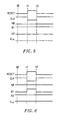
- Figure 5 presents a timing diagram illustrating the operation of the zero current draw circuit in a default (non-bonding option) operating mode.
- the RESET signal is asserted which causes the CLK signal to switch from high to low.
- the logic signal on line 53 (CLK) is passed to the first input of the NAND gate 56, resulting in the signal present on line N1 being high.
- the signal N0 is pulled to low (logic zero) through the n-channel pull-down transistor 60 which is on while N1 is high.
- This logic zero signal is passed through the buffer to the input of the D flip flop 54 on line N2.
- N2 is low.
- the RESET signal is deasserted which causes the CLK signal to switch from low to high.
- the rising edge of the CLK signal enables the D flip flop 54 to pass the signal from line N2, which is low, to D IN .
- D IN stays low after time T2. Since the signal on line 59 is low the pull-down transistor remains on, which keeps the signal N0 at ground potential after time T2.
- the signal on N0 is always low, thus no current is drawn through the n-channel pull-down transistor.
- Figure 6 presents a timing diagram illustrating the operation of the zero current draw circuit when in the bonding option operating mode.
- the bonding pad 30 Since the bonding pad 30 is wire bonded to V CC , the signal on line 51 is always high regardless the status (on or off) of the n-channel pull-down transistor 60. Thus, the signal on line N2 remains high.
- the RESET signal is asserted which makes the CLK signal switch from high to low.
- the logic zero signal on line 53 is present as an input to the NAND gate 56, resulting in line N1 switching from low to high, which turns on the n-channel pull-down transistor 60.
- a leakage current (in the range of a few hundred microamps) is drawn from V CC to V SS through the n-channel pull-down transistor 60 during the period of the RESET signal being high which, in a preferred embodiment, lasts about one millisecond.
- the RESET signal is deasserted which causes the CLK signal to switch from low to high.
- the rising edge of the CLK signal enables the D flip flop 54 to pass the signal present on line N2, which is high, to D IN .
- the signal D IN stays high after time T2.
- the signal on line 53 is high after T2 due to deassertion of RESET.
- the n-channel pull-down transistor 60 is turned off because the output of the NAND gate on line N1 switches from high to low after the deassertion of the RESET signal. Therefore, the leakage current flow from V CC to V SS through the pull-down transistor 60 is cut to approximately zero.
Description
Claims (6)
- A circuit (50) comprising:an input (51 ) for receiving a first signal;an output (DIN) for delivering said first signal;a transistor (60), coupled to said input (51), selectively providing a current path responsive to a second signal; andcircuitry, comprising a D-flip-flop (54) having its D-terminal connected to said input (51) and its clock terminal connected for receiving a reset signal, said circuitry coupled between said transistor (60) and said output (DIN) and providing said second signal by logically combining the reset signal and the output signal of the D-flip-flop.
- The zero current draw circuit of claim 1, wherein said transistor (60) transfers said first signal to ground upon application of said second signal.
- The zero current draw circuit of claim 1, wherein said circuitry further comprises an inverter (58), and a logic element (56), said D-flip-flop (54) being operative to deliver a time shifted version of said first signal.
- The zero current draw circuit of claim 3, wherein said logic element (56) is a NAND gate.
- The zero current draw circuit of claim 1, wherein said input (51) is coupled to a bonding pad.
- The zero current draw circuit of claim 1, wherein said transistor (60) is an n-channel transistor.
Applications Claiming Priority (2)
| Application Number | Priority Date | Filing Date | Title |
|---|---|---|---|
| US876213 | 1997-06-16 | ||
| US08/876,213 US5920227A (en) | 1997-06-16 | 1997-06-16 | Zero current draw circuit for use during a bonding option |
Publications (3)
| Publication Number | Publication Date |
|---|---|
| EP0886380A2 EP0886380A2 (en) | 1998-12-23 |
| EP0886380A3 EP0886380A3 (en) | 2000-02-16 |
| EP0886380B1 true EP0886380B1 (en) | 2005-03-16 |
Family
ID=25367212
Family Applications (1)
| Application Number | Title | Priority Date | Filing Date |
|---|---|---|---|
| EP97309890A Expired - Lifetime EP0886380B1 (en) | 1997-06-16 | 1997-12-08 | Zero current draw circuit for use during a bonding option |
Country Status (4)
| Country | Link |
|---|---|
| US (1) | US5920227A (en) |
| EP (1) | EP0886380B1 (en) |
| JP (1) | JPH1117119A (en) |
| DE (1) | DE69732765T2 (en) |
Families Citing this family (10)
| Publication number | Priority date | Publication date | Assignee | Title |
|---|---|---|---|---|
| TW417267B (en) * | 1997-11-20 | 2001-01-01 | Davicom Semiconductor Inc | Structure of bonding option |
| JP2000223576A (en) * | 1999-02-02 | 2000-08-11 | Rohm Co Ltd | Integrated circuit |
| JP3423904B2 (en) * | 1999-10-06 | 2003-07-07 | 沖電気工業株式会社 | Semiconductor integrated circuit |
| EP1132963B1 (en) | 2000-03-08 | 2007-10-17 | Matsushita Electric Industrial Co., Ltd. | Semiconductor integrated circuit |
| KR100426989B1 (en) * | 2001-06-13 | 2004-04-13 | 삼성전자주식회사 | Control signal providing method using package power pins and IC package structure therefore |
| US7131033B1 (en) | 2002-06-21 | 2006-10-31 | Cypress Semiconductor Corp. | Substrate configurable JTAG ID scheme |
| US7818640B1 (en) | 2004-10-22 | 2010-10-19 | Cypress Semiconductor Corporation | Test system having a master/slave JTAG controller |
| JP2006245063A (en) | 2005-02-28 | 2006-09-14 | Nec Electronics Corp | Semiconductor chip and semiconductor apparatus with semiconductor chip mounted thereon |
| EP2139114A1 (en) * | 2008-06-23 | 2009-12-30 | Dialog Semiconductor GmbH | Ultra-low current push-buttom switch interface circuit |
| WO2016117072A1 (en) * | 2015-01-22 | 2016-07-28 | ルネサスエレクトロニクス株式会社 | Semiconductor device and method for manufacturing same |
Family Cites Families (8)
| Publication number | Priority date | Publication date | Assignee | Title |
|---|---|---|---|---|
| JPS56153832A (en) * | 1980-04-30 | 1981-11-28 | Nec Corp | Digital to analog converter |
| JPH03104315A (en) * | 1989-09-19 | 1991-05-01 | Matsushita Electron Corp | Input terminal potential fixing circuit for cmos semiconductor device |
| JPH0562465A (en) * | 1991-08-30 | 1993-03-12 | Hitachi Ltd | Bonding option circuit and semiconductor integrated circuit |
| EP0573965B1 (en) * | 1992-06-10 | 1999-09-08 | Nec Corporation | Semiconductor device having bonding optional circuit |
| JPH06195476A (en) * | 1992-07-21 | 1994-07-15 | Advanced Micro Devicds Inc | Integrated circuit for incorporation of microcontroller and method for reduction of power consumption by it |
| FR2694851B1 (en) * | 1992-08-12 | 1994-12-23 | Sgs Thomson Microelectronics | Draw circuit to a determined state of an integrated circuit input. |
| EP0670548A1 (en) * | 1994-02-28 | 1995-09-06 | STMicroelectronics, Inc. | Method and structure for recovering smaller density memories from larger density memories |
| US5684411A (en) * | 1995-10-13 | 1997-11-04 | Seiko Communications Systems, Inc. | Self-configuring bus |
-
1997
- 1997-06-16 US US08/876,213 patent/US5920227A/en not_active Expired - Lifetime
- 1997-12-08 EP EP97309890A patent/EP0886380B1/en not_active Expired - Lifetime
- 1997-12-08 DE DE69732765T patent/DE69732765T2/en not_active Expired - Lifetime
- 1997-12-22 JP JP9352749A patent/JPH1117119A/en active Pending
Also Published As
| Publication number | Publication date |
|---|---|
| JPH1117119A (en) | 1999-01-22 |
| DE69732765D1 (en) | 2005-04-21 |
| EP0886380A2 (en) | 1998-12-23 |
| US5920227A (en) | 1999-07-06 |
| DE69732765T2 (en) | 2005-08-11 |
| EP0886380A3 (en) | 2000-02-16 |
Similar Documents
| Publication | Publication Date | Title |
|---|---|---|
| US5414380A (en) | Integrated circuit with an active-level configurable and method therefor | |
| US7358759B2 (en) | Semiconductor device with bus terminating function | |
| KR100309723B1 (en) | Integrated circuit device including cmos tri-state drivers suitable for powerdown | |
| EP0643487B1 (en) | MOS output circuit with leakage current protection | |
| US4963766A (en) | Low-voltage CMOS output buffer | |
| US5723990A (en) | Integrated circuit having high voltage detection circuit | |
| JP3687422B2 (en) | Interface circuit | |
| JPH0855959A (en) | Integrated circuit | |
| EP0886380B1 (en) | Zero current draw circuit for use during a bonding option | |
| US5973511A (en) | Voltage tolerant input/output buffer | |
| US5687122A (en) | Data output buffer | |
| US6150843A (en) | Five volt tolerant I/O buffer | |
| US6335648B1 (en) | Circuit using internal pull-up/pull-down resistor during reset | |
| KR100210557B1 (en) | Input circuit for mode setting | |
| EP0687068A2 (en) | Output driver for use in semiconductor integrated circuit | |
| US5519355A (en) | High speed boundary scan multiplexer | |
| JPH08116250A (en) | Off chip driver circuit | |
| US5594362A (en) | Gatable level-pulling circuit | |
| US5874843A (en) | Power-on reset circuit without an RC Network | |
| US5585759A (en) | Input buffer of semiconductor integrated circuit | |
| US20040001551A1 (en) | Data transmission circuit and method for reducing leakage current | |
| JP3517103B2 (en) | Semiconductor output circuit | |
| JPH0983411A (en) | Semiconductor integrated circuit | |
| US6380795B1 (en) | Semiconductor integrated circuit | |
| US7557604B2 (en) | Input circuit for mode setting |
Legal Events
| Date | Code | Title | Description |
|---|---|---|---|
| PUAI | Public reference made under article 153(3) epc to a published international application that has entered the european phase |
Free format text: ORIGINAL CODE: 0009012 |
|
| AK | Designated contracting states |
Kind code of ref document: A2 Designated state(s): DE FR GB |
|
| AX | Request for extension of the european patent |
Free format text: AL;LT;LV;MK;RO;SI |
|
| PUAL | Search report despatched |
Free format text: ORIGINAL CODE: 0009013 |
|
| AK | Designated contracting states |
Kind code of ref document: A3 Designated state(s): AT BE CH DE DK ES FI FR GB GR IE IT LI LU MC NL PT SE |
|
| AX | Request for extension of the european patent |
Free format text: AL;LT;LV;MK;RO;SI |
|
| RIC1 | Information provided on ipc code assigned before grant |
Free format text: 7H 03K 19/173 A, 7H 03K 19/177 B |
|
| 17P | Request for examination filed |
Effective date: 20000524 |
|
| AKX | Designation fees paid |
Free format text: DE FR GB |
|
| 17Q | First examination report despatched |
Effective date: 20040517 |
|
| GRAP | Despatch of communication of intention to grant a patent |
Free format text: ORIGINAL CODE: EPIDOSNIGR1 |
|
| GRAA | (expected) grant |
Free format text: ORIGINAL CODE: 0009210 |
|
| GRAS | Grant fee paid |
Free format text: ORIGINAL CODE: EPIDOSNIGR3 |
|
| AK | Designated contracting states |
Kind code of ref document: B1 Designated state(s): DE FR GB |
|
| REG | Reference to a national code |
Ref country code: GB Ref legal event code: FG4D |
|
| REF | Corresponds to: |
Ref document number: 69732765 Country of ref document: DE Date of ref document: 20050421 Kind code of ref document: P |
|
| PLBE | No opposition filed within time limit |
Free format text: ORIGINAL CODE: 0009261 |
|
| STAA | Information on the status of an ep patent application or granted ep patent |
Free format text: STATUS: NO OPPOSITION FILED WITHIN TIME LIMIT |
|
| 26N | No opposition filed |
Effective date: 20051219 |
|
| ET | Fr: translation filed | ||
| REG | Reference to a national code |
Ref country code: GB Ref legal event code: 732E Free format text: REGISTERED BETWEEN 20091126 AND 20091202 |
|
| REG | Reference to a national code |
Ref country code: FR Ref legal event code: TP |
|
| PGFP | Annual fee paid to national office [announced via postgrant information from national office to epo] |
Ref country code: FR Payment date: 20101203 Year of fee payment: 14 |
|
| PGFP | Annual fee paid to national office [announced via postgrant information from national office to epo] |
Ref country code: GB Payment date: 20101123 Year of fee payment: 14 |
|
| PGFP | Annual fee paid to national office [announced via postgrant information from national office to epo] |
Ref country code: DE Payment date: 20101230 Year of fee payment: 14 |
|
| GBPC | Gb: european patent ceased through non-payment of renewal fee |
Effective date: 20111208 |
|
| REG | Reference to a national code |
Ref country code: FR Ref legal event code: ST Effective date: 20120831 |
|
| REG | Reference to a national code |
Ref country code: DE Ref legal event code: R119 Ref document number: 69732765 Country of ref document: DE Effective date: 20120703 |
|
| PG25 | Lapsed in a contracting state [announced via postgrant information from national office to epo] |
Ref country code: DE Free format text: LAPSE BECAUSE OF NON-PAYMENT OF DUE FEES Effective date: 20120703 Ref country code: GB Free format text: LAPSE BECAUSE OF NON-PAYMENT OF DUE FEES Effective date: 20111208 |
|
| PG25 | Lapsed in a contracting state [announced via postgrant information from national office to epo] |
Ref country code: FR Free format text: LAPSE BECAUSE OF NON-PAYMENT OF DUE FEES Effective date: 20120102 |