EP0884777B1 - Method for manufacturing semiconductor memory device - Google Patents
Method for manufacturing semiconductor memory device Download PDFInfo
- Publication number
- EP0884777B1 EP0884777B1 EP98300304A EP98300304A EP0884777B1 EP 0884777 B1 EP0884777 B1 EP 0884777B1 EP 98300304 A EP98300304 A EP 98300304A EP 98300304 A EP98300304 A EP 98300304A EP 0884777 B1 EP0884777 B1 EP 0884777B1
- Authority
- EP
- European Patent Office
- Prior art keywords
- layer
- insulating layer
- forming
- bit lines
- contact hole
- Prior art date
- Legal status (The legal status is an assumption and is not a legal conclusion. Google has not performed a legal analysis and makes no representation as to the accuracy of the status listed.)
- Expired - Lifetime
Links
Images



Classifications
-
- H—ELECTRICITY
- H10—SEMICONDUCTOR DEVICES; ELECTRIC SOLID-STATE DEVICES NOT OTHERWISE PROVIDED FOR
- H10B—ELECTRONIC MEMORY DEVICES
- H10B12/00—Dynamic random access memory [DRAM] devices
- H10B12/01—Manufacture or treatment
- H10B12/02—Manufacture or treatment for one transistor one-capacitor [1T-1C] memory cells
- H10B12/03—Making the capacitor or connections thereto
- H10B12/033—Making the capacitor or connections thereto the capacitor extending over the transistor
-
- H—ELECTRICITY
- H10—SEMICONDUCTOR DEVICES; ELECTRIC SOLID-STATE DEVICES NOT OTHERWISE PROVIDED FOR
- H10D—INORGANIC ELECTRIC SEMICONDUCTOR DEVICES
- H10D64/00—Electrodes of devices having potential barriers
- H10D64/01—Manufacture or treatment
- H10D64/011—Manufacture or treatment of electrodes ohmically coupled to a semiconductor
-
- H—ELECTRICITY
- H10—SEMICONDUCTOR DEVICES; ELECTRIC SOLID-STATE DEVICES NOT OTHERWISE PROVIDED FOR
- H10B—ELECTRONIC MEMORY DEVICES
- H10B12/00—Dynamic random access memory [DRAM] devices
- H10B12/01—Manufacture or treatment
- H10B12/02—Manufacture or treatment for one transistor one-capacitor [1T-1C] memory cells
- H10B12/03—Making the capacitor or connections thereto
- H10B12/033—Making the capacitor or connections thereto the capacitor extending over the transistor
- H10B12/0335—Making a connection between the transistor and the capacitor, e.g. plug
-
- H—ELECTRICITY
- H10—SEMICONDUCTOR DEVICES; ELECTRIC SOLID-STATE DEVICES NOT OTHERWISE PROVIDED FOR
- H10B—ELECTRONIC MEMORY DEVICES
- H10B12/00—Dynamic random access memory [DRAM] devices
- H10B12/30—DRAM devices comprising one-transistor - one-capacitor [1T-1C] memory cells
- H10B12/48—Data lines or contacts therefor
- H10B12/482—Bit lines
Definitions
- the present invention relates to a method for manufacturing a semiconductor device, and a semiconductor memory device, and more particularly, to a method for manufacturing a semiconductor memory device that is resistant to oxidation of the bit lines, and a semiconductor memory device.
- a bit line is generally formed by a polycide structure obtained by depositing an impurity-doped polysilicon and a low-resistance silicide.
- FIG. 1 is a sectional view for explaining a method for manufacturing a conventional DRAM.
- a transistor (not shown) is formed by a conventional manner on a semiconductor substrate 100 divided into an active regions (not shown) and field regions (not shown) by field oxide layers 12.
- polysilicon is deposited on the resultant structure and then patterned, thereby forming a pad 14 for connecting a storage electrode to the active region (source region) of the semiconductor substrate 100.
- an insulating material is deposited on the resultant structure and then planarized, thereby forming a first insulating layer 16 for insulating the transistor from another conductive layer.
- the first insulating layer 16 may be formed of a fluid insulating layer, e.g., borophosphosilicate glass (BPSG) or undoped silicate glass (USG).
- BPSG borophosphosilicate glass
- USG undoped silicate glass
- bit line contact (not shown) and bit line 18 and 20 is formed by a conventional method and then a planarized second insulating layer 22 is formed on the resultant structure.
- the bit line is formed by depositing a doped polysilicon layer 18 and a silicide layer 20 on the first insulating layer 16, and the second insulating layer 22 is formed in a similar manner to the first insulating layer 16. Subsequently, a nitride layer 24 and an oxide layer 26 are sequentially deposited on the resultant structure.
- the oxide layer 26, the nitride layer 24, the second insulating layer 22 and the first insulating layer 16 are anisotropically etched by photolithography to form a contact hole exposing the pad 14.
- a nitride layer is deposited on the surface of the resultant structure having the contact hole to form a spacer 28 on the sidewall of the contact hole. The spacer 28 helps prevent the oxidation of the bit lines by oxygen diffused through the sidewall of the contact hole.
- a polysilicon layer is deposited on the resultant structure, and patterned by photolithography to form a storage electrode 30.
- a dielectric layer 32 and a plate electrode 34 are formed on the storage electrode 30 by a conventional method.
- the dielectric layer 32 may be formed in an NO structure obtained by depositing a nitride layer and by forming a thermal oxide layer, for the purpose of improving capacitor characteristics.
- the nitride layer is typically formed by a chemical vapor deposition (CVD) method, and the oxide layer is formed by a thermal oxidation method.
- Other types of dielectrics such as ONO may also be used.
- FIG. 2 is a sectional view showing an example of such misalignment.
- misalignment occurs between the etching mask for storage electrode 30 and the contact hole, an overetch may occur on the nitride layer spacer 28 when the storage electrode 30 is patterned by etching. Accordingly, the second insulating layer 22 is exposed at the sidewall of the contact hole. If the second insulating layer 22 is exposed, the nitride layer is deposited more thinly on the exposed second insulating layer 22 than on other layers when the dielectric layer 32 is formed in a subsequent step. This phenomenon is caused by the different deposition rates of the nitride layer, depending on the composition of the underlayer.
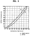
- FIG. 3 shows the deposition characteristics of the nitride layer for both a wafer underlayer and a BPSG underlayer.
- "A” indicates the thickness of the nitride layer deposited on a bare wafer
- "B” indicates the thickness of the nitride layer deposited on a BPSG layer.
- the graph for a deposition time of 50 minutes when the nitride layer is deposited on the bare wafer to a thickness of about 50 angstroms, the nitride layer is deposited to be only 37 angstroms thick on the BPSG layer. Therefore, as shown in FIG.
- the second insulating layer 22 is susceptible to oxygen diffusion because the oxygen used during thermal oxidation in forming the oxide in the dielectric layer 34 may penetrate into a portion of second insulating layer 22 where the nitride layer is deposited thinly.
- the bit line 18 and 20 may become oxidized, thereby changing its electrical characteristics. The resulting increased resistance in the bit line may cause the memory device to become inoperative or unreliable.
- US-A-5126280 and US-A-5196364 relate to semiconductor circuit memory storage devices in which an oxidation prevention layer such as a nitride layer is used to prevent bit line attack during subsequent processing.
- an oxidation prevention layer such as a nitride layer is used to prevent bit line attack during subsequent processing.
- US-A-5330614 discloses a semiconductor memory device in which, in one embodiment, a nitride layer and an oxide layer are sequentially stacked on the whole surface of a semiconductor substrate having a contact hole.
- EP-A-0539233 also relates to manufacture of a semiconductor device in which a lower electrode is subjected to rapid heat-treatment with optional formation of a nitrided layer.
- US-A-5445999 relates to a method for fabricating an ultrathin film, dielectric layer over a silicon or polysilicon semiconductor substrate.
- a method for manufacturing a semiconductor memory device including the step of forming first insulating layer on a semiconductor substrate. Bit lines connected to the semiconductor substrate are formed on the first insulating layer. Then, an oxidation preventing layer is formed on the resultant structure. A second insulating layer is formed on the oxidation preventing layer and a contact hole exposing a portion of the semiconductor substrate is formed. A storage electrode connected to the portion of the semiconductor substrate through the contact hole is formed. A dielectric layer and a plate electrode are sequentially formed on the storage electrode.
- bit lines may be formed by the sequential deposition and patterning of polysilicon and silicide, or the bit lines may be formed of other suitable conductors.
- the nitride layer may be formed using a low pressure chemical vapor deposition (LPCVD) process, a rapid thermal nitridation (RTN) process, or by other processes for forming a nitride layer.
- LPCVD low pressure chemical vapor deposition
- RTN rapid thermal nitridation
- the LPCVD process may be performed at a temperature of about 500 ⁇ 700° C under a pressure of about 1 torr or less using a gas mixture of dichlorosilane (SiH 2 Cl 2 ) and ammonia (NH 3 ) as a reactant gas.
- the RTN process is preferably performed at a temperature of about 800 ⁇ 1000° C under atmospheric pressure or less using an ammonia (NH 3 ) gas as a reactant gas.
- the oxidation preventing layer may be formed by nitriding the surface of the resultant structure containing the bit lines using a gas containing nitrogen.
- a gas containing nitrogen An ammonia (NH 3 ) or similar gas may be used as the gas containing the nitrogen, and a plasma method, a thermal annealing method, or a rapid thermal process (RTP) may be employed.
- NH 3 ammonia
- RTP rapid thermal process
- the oxidation preventing layer may be formed to be thicker at the side walls and on top of the bit line than on the surface of the second insulating layer.
- the step of forming the dielectric layer comprises the steps of depositing a nitride layer on the storage electrode, and oxidizing the semiconductor substrate having the nitride layer under a wet-oxidative atmosphere.
- the wet oxidation is preferably performed at a temperature of about 700 ⁇ 900° C.
- a spacer is formed on the sidewall of the contact hole before forming the storage electrode.
- a method for manufacturing a semiconductor memory device including the step of forming a first insulating layer on a semiconductor substrate. Bit lines are formed on the first insulating layer and a second insulating layer is formed on the resultant structure. A contact hole exposing a portion of the semiconductor substrate is formed. A storage electrode connected to the portion of the semiconductor substrate through the contact hole is formed. An oxidation preventing layer is formed on the surface of the structure containing the storage electrode. A dielectric layer and a plate electrode are sequentially formed on the resultant structure.
- the bit lines may be formed by sequentially depositing and patterning polysilicon and silicide.
- the oxidation preventing layer may be formed by nitriding the surface of the resultant structure having the storage electrode using a gas containing nitrogen.
- An ammonia (NH 3 ) or similar gas may be used as the gas containing the nitrogen.
- the nitridation process may be performed using a plasma method, a thermal annealing method, a rapid thermal process (RTP), or a similar process.
- the step of forming the dielectric layer comprises the steps of depositing a nitride layer on the resultant structure having the storage electrode, and oxidizing the nitride layer under a wet-oxidative atmosphere.
- the wet oxidation is preferably performed at a temperature of about 700 ⁇ 900° C.
- a spacer is formed on the sidewall of the contact hole before forming the storage electrode.
- a first insulating layer is formed on a semiconductor substrate.
- Bit lines connected to a first active region of the semiconductor substrate are formed on the first insulating laver.
- An oxidation preventing layer is formed to wrap the bit lines and to be thicker at the side walls and on top of the bit lines than on the surface of the first insulating layer.
- a second insulating layer is formed to cover the oxidation preventing layer.
- a storage electrode connected to a second active region of the semiconductor substrate through a contact hole formed by etching the second insulating layer, oxidation preventing layer and first insulating layer, is formed, and a dielectric layer covering the storage electrode and a plate electrode covering the dielectric layer are sequentially formed.
- the oxidation preventing layer is formed of a nitride layer and the thickness thereof is less than 1,000 angstroms.
- a spacer is further formed on the inner sidewall of the contact hole, and the dielectric layer is preferably formed of a dual layer comprised of a nitride layer and an oxide layer.
- the bit lines may be prevented from being oxidized in the course of forming a dielectric layer, that is, the oxidation prevention layer is for maintaining the same conductivity as the initial conductivity of the bit line. Also, this process allows the subsequent step of forming the dielectric to be performed easily.
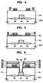
- FIGs. 4 through 7 are sectional views for explaining a method of forming a semiconductor memory device according to a first embodiment of the present invention.
- FIG. 4 shows the steps of forming a transistor (not shown), a pad 42 and a bit line 46 and 48.
- Field oxide layers 40 divide a semiconductor substrate 200 into active regions (not shown). The field oxide is formed by a conventional isolation technology. Then, a transistor (not shown) having a gate, a source and a drain (not shown) is formed in the active region of the semiconductor substrate 200.
- the semiconductor substrate is typically polysilicon, although it may be formed of other semiconductor material. Polysilicon is then deposited on the resultant structure having the transistor and is patterned, thereby forming a pad 42 connected to the source (not shown) of the transistor.
- the first insulating layer 44 is deposited on the resultant structure and is planarized, thereby forming a first insulating layer 44 for insulating the transistor from other conductive layers.
- the first insulating layer 44 may be formed of a borophosphosilicate glass (BPSG) layer, an undoped silicate glass (USG) layer, or another suitable insulating material
- the first insulating layer 44 is partially etched to form a contact hole (not shown) exposing the drain (not shown) of the transistor.
- a doped polysilicon layer and a silicide layer are sequentially formed on the resultant structure and then patterned, thereby forming bit lines 46 and 48, which are connected to the transistor drains through contact holes (not shown).
- FIG. 5 shows the step of forming an oxidation preventing layer 50 for preventing oxidation of the bit lines 46 and 48.
- An insulating material for preventing oxidation e.g., a nitride layer, is deposited over the entire surface of the resultant structure comprising the first insulating layer 44 and bit lines 46 and 48, thereby forming the oxidation preventing layer 50.
- the oxidation preventing layer 50 serves to prevent oxidation of the bit lines 46 and 48 during a subsequent oxidation process associated with forming a dielectric layer for a capacitor.
- the oxidation preventing layer 50 is preferably formed to be thick enough to prevent oxidation of the bit line 46 and 48, e.g., to a thickness of 1,000 angstroms or less.
- FIG. 6 shows the steps of and forming a contact hole 58 and forming a spacer 60.
- An insulating layer which may be easily planarized, e.g., a BPSG or USG layer, is deposited over the entire surface of the resultant structure having the oxidation preventing layer 50 and then flowed, thereby forming a second insulating layer 52.
- the second insulating layer 52 not only insulates the bit line 46 and 48 from other conductive layers but also planarizes the step that occurs due to the height of the bit line 46 and 48, thereby facilitating subsequent processes.
- a nitride layer 54 of about 500 angstroms thickness and an oxide layer 56 of about 2,000 angstroms thickness are sequentially deposited on the resultant structure.
- the oxide layer 56, the nitride layer 54, the second insulating layer 52, the oxidation preventing layer 50 and the first insulating layer 44 are sequentially anisotropically etched by photolithography, thereby forming a contact hole 58 for connecting the storage electrode to the pad 42.
- a nitride layer having a thickness of 500 angstroms or less is deposited on the resultant structure and then anisotropically etched, thereby forming the spacer 60 at the inner side walls of the contact hole 58.
- the spacer 60 is for preventing the bit lines 46 and 48 from being oxidized from the sidewall of the contact hole 58.
- FIG. 7 shows the step of forming a capacitor comprised of a storage electrode 62, a dielectric layer 64, and a plate electrode 66.
- a doped polysilicon layer is deposited to a predetermined thickness over the entire surface of the resultant structure having the spacer 60 and then anisotropically etched to form the storage electrode 62 connected to the pad 42.
- the dielectric layer 64 for a capacitor is formed.
- a thin nitride layer is first deposited over the entire surface of the resultant structure having the storage electrode 62.
- the nitride layer is deposited thinly on the area where the second insulating layer 52 is exposed, as compared with the thickness of the nitride layer deposited the other structures. Thereafter, the nitride dielectric layer is oxidized under a wet-oxidation atmosphere at a high temperature of about 700 ⁇ 900° C, thereby forming an oxide layer on the nitride layer.
- the bit lines 46 and 48 are oxidized by oxygen (O 2 ) diffused through a portion of the first insulating layer where the nitride layer for a dielectric layer is deposited thinly during the oxidation step.
- oxygen O 2
- the bit lines 46 and 48 are protected from oxidation because they are surrounded by the oxidation preventing layer 50.
- a doped polysilicon layer is deposited on the resultant structure having the dielectric layer 64 and then patterned, thereby forming the plate electrode 66.
- FIG. 8 is a sectional view for explaining a method for forming a semiconductor memory device according to a second embodiment of the present invention.
- those elements which are the same as those of FIG. 7 are designated by the same reference numerals.
- Oxidation of bit lines can be prevented, by depositing a thin nitride layer (about 70 angstroms) serving as an oxygen diffusion preventing layer, before forming an insulating layer after forming the bit lines, and depositing the insulating layer thereon.
- this method may cause a severe impediment to a self-aligned contact (SAC) process in a subsequent process, i.e., a process of forming a contact hole for connecting a storage electrode and a semiconductor substrate.
- SAC self-aligned contact
- the nitride layer may readily cause etching stop or produce a sill or ledge on the top of the contact hole.
- an aspect ratio of the contact hole increases.
- a device having a fast etch rate such as a high density plasma is widely adopted. Since the selectivity for the nitride layer is also high in this case, the contact hole may not open completely, which readily causes malfunction.
- oxidation preventing layer 50 for preventing oxidation of bit lines 46 and 48 such as a nitride layer
- bit lines 46 and 48 such as a nitride layer
- nitride layer is deposited such that the nitride layer is deposited more thickly on the sidewalls and the top of the bit lines, and is deposited thinly on the first insulting layer 44. If the nitride layer is deposited as an oxidation preventing layer 50 using a LPCVD method or a RTN method, initial layer growth rates of the nitride layer may differ depending on the physical properties of the bit line and the insulating layer.
- the nitride layer is deposited more thinly on the first insulating layer 44 comprising BPSG or USG.
- the reason for the foregoing is that it is difficult to attain initial nucleation of the nitride layer on the BPSG layer.
- the nitride layer is deposited on the bit lines to a thickness of about 50 angstroms, the nitride layer is deposited on the BPSG layer to a thickness of about 10-20 angstroms.
- the oxidation preventing layer 50 is preferably deposited under a pressure of 1 torr or less at a temperature of 900 ⁇ 100° C using a mixed gas of dichlorosilane (SiH 2 Cl 2 ) and ammonia (NH 3 ) as a reactant gas. If the RTN method is employed, the oxidation preventing layer is deposited at a temperature of 900 ⁇ 100° C using an ammonia (NH 3 ) gas as a reactant gas, and is preferably deposited under atmospheric pressure or a lower pressure.
- FIG. 9 is a sectional view for explaining a method of forming a semiconductor memory device according to a fourth embodiment of the present invention.
- those elements which are the same as those in the first embodiment are designated by the same reference numerals.
- the same steps as those in the first embodiment are performed until the bit lines 46 and 48 are formed.
- the surface of the resultant structure having the first insulating layer 44 and bit lines 46 and 48 is nitrided using a nitrogen-containing gas.
- a thin nitride layer 80 is formed on the surface of the resultant structure, as shown. Therefore, the same effects as in the first and second embodiments can be obtained.
- nitride layer 80 formed by nitridation is very thin, i.e., 30-50 angstroms, a nitride sill or ledge is not produced on the sidewall of the contact hole when the contact hole is etched.
- the surface of the resultant structure having the bit lines 46 and 48 may be processed by using a plasma method, a thermal annealing method, an RTP, or a similar process.
- a gas containing nitrogen, such as ammonia (NH 3 ) gas, can be used as a reactant gas.
- the plasma method is preferably performed at a temperature of 200 ⁇ 400° C for more than 1 minute.
- the thermal annealing method is preferably performed at a temperature of 800 ⁇ 900° C for more than 30 minutes.
- the RTP is preferably performed at a temperature of 800 ⁇ 1000° C for more than 1 minute. The temperatures and times associated with these processes may be varied to achieve the desired nitridation result.
- FIG. 10 is a sectional view for explaining a method of forming a semiconductor memory device not forming part of the present claimed invention.
- those elements which are the same as those of the first embodiment are designated by the same reference numerals.
- the same steps as those in the first embodiment are performed until a storage electrode 62 is formed, with the exception that the oxidation preventing layer 50 in the first embodiment is not formed.
- the surface of the second insulating layer 52 in the upper portion of the contact hole is exposed.
- the surface of the resultant structure having the storage electrode 62 is nitrided using a gas containing nitrogen by the same method as in the fourth embodiment.
- a thin nitride layer 85 having a thickness of about 30-50 angstroms is formed on the surface of the resultant structure.
- a dielectric layer 64 and a plate electrode 66 are formed.
- the surface of the resultant structure may be processed by using a plasma method, a thermal annealing method, an RTP, or a similar method.
- a gas containing nitrogen, such as ammonia (NH 3 ) gas, may be used as a reactant gas.
- the surface of the resultant structure is nitrided after forming the storage electrode 62
- the surface of the exposed second insulating layer 52 is also nitrided. Accordingly, since a nitride layer for a dielectric layer 64 is formed on nitrided underlayers during a step of forming the dielectric layer, the dielectric layer may be formed more thickly rather than being dependent on the individual properties of the different underlayers. Therefore, the nitride layer for a dielectric layer is deposited on the surface of the second insulating layer 52 as thickly as or thicker than on the surface of the storage electrode 62. Therefore, the bit line oxidation due to diffused oxygen can be prevented when the oxide layer in the dielectric is subsequently formed.
- FIG. 11 is a graph for comparing the thicknesses of the nitride layers deposited on a BPSG layer before and after nitridation the surface of the BPSG layer. The nitridation is performed for the purpose of eliminating the dependence of the nitride layer on the composition of the underlayer.
- 1 indicates the case of omitting a surface processing
- 2 indicates the case of performing a plasma process at a temperature of 400° C for 240 seconds using an ammonia (NH 3 ) gas
- 3 indicates the case of performing an RTN process at a temperature of 800° C for 90 seconds
- 4 indicates the case of performing an RTN process at a temperature of 1,000° C for 90 seconds
- 5 indicates the case of performing a thermal annealing process at a temperature of 820° C for 60 minutes using an ammonia (NH 2 ) gas.
- the nitride layer is deposited thicker in the case of depositing the same after processing the surface than in the case of omitting the surface processing. Therefore, surface processing by nitriding the surface of the storage electrode structure tends to eliminate the dependence on the underlayer of the nitride layer thickness in the dielectric layer 64, so that the nitride layer is deposited on the surface of the exposed second insulating layer (52 of FIG. 12) as thickly as or thicker than on the surface of the storage electrode (62 of FIG. 10).
- an oxidation preventing layer is formed on the resultant structure.
- a dual spacer may be formed on the sidewall of the contact hole. Accordingly, even if misalignment occurs when patterning the storage electrode, the bit lines may be prevented from being oxidized by oxygen diffused through the sidewall of the contact hole during the formation of a dielectric layer. Particularly, by nitriding the surface of the resultant structure obtained after forming the bit lines or storage electrodes, the oxidation of the bit lines may be prevented.
Landscapes
- Engineering & Computer Science (AREA)
- Manufacturing & Machinery (AREA)
- Internal Circuitry In Semiconductor Integrated Circuit Devices (AREA)
- Semiconductor Memories (AREA)
Description
- The present invention relates to a method for manufacturing a semiconductor device, and a semiconductor memory device, and more particularly, to a method for manufacturing a semiconductor memory device that is resistant to oxidation of the bit lines, and a semiconductor memory device.
- In manufacturing a dynamic random access memory (DRAM), to increase the operational speed of a device, a bit line is generally formed by a polycide structure obtained by depositing an impurity-doped polysilicon and a low-resistance silicide.
- FIG. 1 is a sectional view for explaining a method for manufacturing a conventional DRAM.
- Referring to FIG. 1, a transistor (not shown) is formed by a conventional manner on a
semiconductor substrate 100 divided into an active regions (not shown) and field regions (not shown) byfield oxide layers 12. Next, polysilicon is deposited on the resultant structure and then patterned, thereby forming apad 14 for connecting a storage electrode to the active region (source region) of thesemiconductor substrate 100. After the pad is formed, an insulating material is deposited on the resultant structure and then planarized, thereby forming a first insulatinglayer 16 for insulating the transistor from another conductive layer. To facilitate the planarization, thefirst insulating layer 16 may be formed of a fluid insulating layer, e.g., borophosphosilicate glass (BPSG) or undoped silicate glass (USG). - Next, a bit line contact (not shown) and
bit line insulating layer 22 is formed on the resultant structure. The bit line is formed by depositing a dopedpolysilicon layer 18 and asilicide layer 20 on the first insulatinglayer 16, and the secondinsulating layer 22 is formed in a similar manner to the firstinsulating layer 16. Subsequently, anitride layer 24 and anoxide layer 26 are sequentially deposited on the resultant structure. - Next, the
oxide layer 26, thenitride layer 24, the secondinsulating layer 22 and the firstinsulating layer 16 are anisotropically etched by photolithography to form a contact hole exposing thepad 14. A nitride layer is deposited on the surface of the resultant structure having the contact hole to form aspacer 28 on the sidewall of the contact hole. Thespacer 28 helps prevent the oxidation of the bit lines by oxygen diffused through the sidewall of the contact hole. - Next, a polysilicon layer is deposited on the resultant structure, and patterned by photolithography to form a
storage electrode 30. A dielectric layer 32 and a plate electrode 34 are formed on thestorage electrode 30 by a conventional method. The dielectric layer 32 may be formed in an NO structure obtained by depositing a nitride layer and by forming a thermal oxide layer, for the purpose of improving capacitor characteristics. The nitride layer is typically formed by a chemical vapor deposition (CVD) method, and the oxide layer is formed by a thermal oxidation method. Other types of dielectrics such as ONO may also be used. - As semiconductor memory devices become highly integrated, misalignment may occur during the photolithography for forming the
storage electrode 30. FIG. 2 is a sectional view showing an example of such misalignment. In FIG. 2, if misalignment occurs between the etching mask forstorage electrode 30 and the contact hole, an overetch may occur on thenitride layer spacer 28 when thestorage electrode 30 is patterned by etching. Accordingly, the secondinsulating layer 22 is exposed at the sidewall of the contact hole. If the secondinsulating layer 22 is exposed, the nitride layer is deposited more thinly on the exposed secondinsulating layer 22 than on other layers when the dielectric layer 32 is formed in a subsequent step. This phenomenon is caused by the different deposition rates of the nitride layer, depending on the composition of the underlayer. - FIG. 3 shows the deposition characteristics of the nitride layer for both a wafer underlayer and a BPSG underlayer. In FIG. 3, "A" indicates the thickness of the nitride layer deposited on a bare wafer, and "B" indicates the thickness of the nitride layer deposited on a BPSG layer. As shown in the graph for a deposition time of 50 minutes, when the nitride layer is deposited on the bare wafer to a thickness of about 50 angstroms, the nitride layer is deposited to be only 37 angstroms thick on the BPSG layer. Therefore, as shown in FIG. 2, the second
insulating layer 22 is susceptible to oxygen diffusion because the oxygen used during thermal oxidation in forming the oxide in the dielectric layer 34 may penetrate into a portion of secondinsulating layer 22 where the nitride layer is deposited thinly. Thebit line - US-A-5126280 and US-A-5196364 relate to semiconductor circuit memory storage devices in which an oxidation prevention layer such as a nitride layer is used to prevent bit line attack during subsequent processing.
- US-A-5330614 discloses a semiconductor memory device in which, in one embodiment, a nitride layer and an oxide layer are sequentially stacked on the whole surface of a semiconductor substrate having a contact hole.
- EP-A-0539233 also relates to manufacture of a semiconductor device in which a lower electrode is subjected to rapid heat-treatment with optional formation of a nitrided layer.
- US-A-5445999 relates to a method for fabricating an ultrathin film, dielectric layer over a silicon or polysilicon semiconductor substrate.
- To accomplish the above object of the present invention as claimed in
claim 1, there is provided a method for manufacturing a semiconductor memory device including the step of forming first insulating layer on a semiconductor substrate. Bit lines connected to the semiconductor substrate are formed on the first insulating layer. Then, an oxidation preventing layer is formed on the resultant structure. A second insulating layer is formed on the oxidation preventing layer and a contact hole exposing a portion of the semiconductor substrate is formed. A storage electrode connected to the portion of the semiconductor substrate through the contact hole is formed. A dielectric layer and a plate electrode are sequentially formed on the storage electrode. - The bit lines may be formed by the sequential deposition and patterning of polysilicon and silicide, or the bit lines may be formed of other suitable conductors.
- The oxidation preventing layer may be formed of a nitride layer and is preferably formed to a thickness of about 1,000 angstroms (10Å=1nm) or below. The nitride layer may be formed using a low pressure chemical vapor deposition (LPCVD) process, a rapid thermal nitridation (RTN) process, or by other processes for forming a nitride layer. The LPCVD process may be performed at a temperature of about 500~700° C under a pressure of about 1 torr or less using a gas mixture of dichlorosilane (SiH2Cl2) and ammonia (NH3) as a reactant gas. The RTN process is preferably performed at a temperature of about 800∼1000° C under atmospheric pressure or less using an ammonia (NH3) gas as a reactant gas.
- The oxidation preventing layer may be formed by nitriding the surface of the resultant structure containing the bit lines using a gas containing nitrogen. An ammonia (NH3) or similar gas may be used as the gas containing the nitrogen, and a plasma method, a thermal annealing method, or a rapid thermal process (RTP) may be employed.
- The oxidation preventing layer may be formed to be thicker at the side walls and on top of the bit line than on the surface of the second insulating layer.
- The step of forming the dielectric layer comprises the steps of depositing a nitride layer on the storage electrode, and oxidizing the semiconductor substrate having the nitride layer under a wet-oxidative atmosphere. The wet oxidation is preferably performed at a temperature of about 700~900° C.
- A spacer is formed on the sidewall of the contact hole before forming the storage electrode.
- According to still another aspect of the present invention, there is provided a method for manufacturing a semiconductor memory device including the step of forming a first insulating layer on a semiconductor substrate. Bit lines are formed on the first insulating layer and a second insulating layer is formed on the resultant structure. A contact hole exposing a portion of the semiconductor substrate is formed. A storage electrode connected to the portion of the semiconductor substrate through the contact hole is formed. An oxidation preventing layer is formed on the surface of the structure containing the storage electrode. A dielectric layer and a plate electrode are sequentially formed on the resultant structure.
- The bit lines may be formed by sequentially depositing and patterning polysilicon and silicide.
- The oxidation preventing layer may be formed by nitriding the surface of the resultant structure having the storage electrode using a gas containing nitrogen. An ammonia (NH3) or similar gas may be used as the gas containing the nitrogen. Also, the nitridation process may be performed using a plasma method, a thermal annealing method, a rapid thermal process (RTP), or a similar process.
- The step of forming the dielectric layer comprises the steps of depositing a nitride layer on the resultant structure having the storage electrode, and oxidizing the nitride layer under a wet-oxidative atmosphere. The wet oxidation is preferably performed at a temperature of about 700~900° C.
- A spacer is formed on the sidewall of the contact hole before forming the storage electrode.
- According to still yet another aspect of the present invention as claimed in claim 15, a first insulating layer is formed on a semiconductor substrate. Bit lines connected to a first active region of the semiconductor substrate are formed on the first insulating laver. An oxidation preventing layer is formed to wrap the bit lines and to be thicker at the side walls and on top of the bit lines than on the surface of the first insulating layer. A second insulating layer is formed to cover the oxidation preventing layer. A storage electrode connected to a second active region of the semiconductor substrate through a contact hole formed by etching the second insulating layer, oxidation preventing layer and first insulating layer, is formed, and a dielectric layer covering the storage electrode and a plate electrode covering the dielectric layer are sequentially formed.
- It is preferable that the oxidation preventing layer is formed of a nitride layer and the thickness thereof is less than 1,000 angstroms.
- A spacer is further formed on the inner sidewall of the contact hole, and the dielectric layer is preferably formed of a dual layer comprised of a nitride layer and an oxide layer.
- According to the present invention, even if misalignment occurs in patterning a storage electrode, the bit lines may be prevented from being oxidized in the course of forming a dielectric layer, that is, the oxidation prevention layer is for maintaining the same conductivity as the initial conductivity of the bit line. Also, this process allows the subsequent step of forming the dielectric to be performed easily.
- The above object and advantages of the present invention will become more apparent by describing in detail preferred embodiments thereof by reference to the attached drawings in which:
- FIG. 1 is a sectional view taken in a direction of a word line, for explaining a method for forming a conventional DRAM;
- FIG. 2 is a sectional view showing a situation in which misalignment occurs during photolithography for forming a storage electrode;
- FIG. 3 is a graph showing deposition characteristics of a nitride layer depending on the underlayer composition;
- FIGs. 4 through 7 are sectional views for explaining a method of forming a semiconductor memory device according to a first embodiment of the present invention;
- FIG. 8 is a sectional view for explaining a method of forming a semiconductor memory device according to a second embodiment of the present invention;
- FIG. 9 is a sectional view for explaining a method of forming a semiconductor memory device according to a third embodiment of the present invention;
- FIG. 10 is a sectional view for explaining a method of forming a semiconductor memory device a not forming part of the present claimed invention; and
- FIG. 11 is a graph that compares the thicknesses of a nitride layer deposited on a BPSG layer depending on the surface processing used before depositing the nitride layer.
- FIGs. 4 through 7 are sectional views for explaining a method of forming a semiconductor memory device according to a first embodiment of the present invention.
- FIG. 4 shows the steps of forming a transistor (not shown), a
pad 42 and abit line semiconductor substrate 200 into active regions (not shown). The field oxide is formed by a conventional isolation technology. Then, a transistor (not shown) having a gate, a source and a drain (not shown) is formed in the active region of thesemiconductor substrate 200. The semiconductor substrate is typically polysilicon, although it may be formed of other semiconductor material. Polysilicon is then deposited on the resultant structure having the transistor and is patterned, thereby forming apad 42 connected to the source (not shown) of the transistor. An insulating layer is deposited on the resultant structure and is planarized, thereby forming a first insulatinglayer 44 for insulating the transistor from other conductive layers. To facilitate the planarization, the first insulatinglayer 44 may be formed of a borophosphosilicate glass (BPSG) layer, an undoped silicate glass (USG) layer, or another suitable insulating material - Next, the first insulating
layer 44 is partially etched to form a contact hole (not shown) exposing the drain (not shown) of the transistor. A doped polysilicon layer and a silicide layer are sequentially formed on the resultant structure and then patterned, thereby formingbit lines - FIG. 5 shows the step of forming an
oxidation preventing layer 50 for preventing oxidation of the bit lines 46 and 48. An insulating material for preventing oxidation, e.g., a nitride layer, is deposited over the entire surface of the resultant structure comprising the first insulatinglayer 44 andbit lines oxidation preventing layer 50. Theoxidation preventing layer 50 serves to prevent oxidation of the bit lines 46 and 48 during a subsequent oxidation process associated with forming a dielectric layer for a capacitor. In this embodiment, theoxidation preventing layer 50 is preferably formed to be thick enough to prevent oxidation of thebit line - FIG. 6 shows the steps of and forming a
contact hole 58 and forming aspacer 60. An insulating layer which may be easily planarized, e.g., a BPSG or USG layer, is deposited over the entire surface of the resultant structure having theoxidation preventing layer 50 and then flowed, thereby forming a second insulatinglayer 52. The second insulatinglayer 52 not only insulates thebit line bit line nitride layer 54 of about 500 angstroms thickness and anoxide layer 56 of about 2,000 angstroms thickness are sequentially deposited on the resultant structure. - Subsequently, the
oxide layer 56, thenitride layer 54, the second insulatinglayer 52, theoxidation preventing layer 50 and the first insulatinglayer 44 are sequentially anisotropically etched by photolithography, thereby forming acontact hole 58 for connecting the storage electrode to thepad 42. Next, a nitride layer having a thickness of 500 angstroms or less is deposited on the resultant structure and then anisotropically etched, thereby forming thespacer 60 at the inner side walls of thecontact hole 58. Thespacer 60 is for preventing the bit lines 46 and 48 from being oxidized from the sidewall of thecontact hole 58. - FIG. 7 shows the step of forming a capacitor comprised of a storage electrode 62, a dielectric layer 64, and a
plate electrode 66. A doped polysilicon layer is deposited to a predetermined thickness over the entire surface of the resultant structure having thespacer 60 and then anisotropically etched to form the storage electrode 62 connected to thepad 42. Subsequently, the dielectric layer 64 for a capacitor is formed. To form the dielectric layer 64, a thin nitride layer is first deposited over the entire surface of the resultant structure having the storage electrode 62. At this point, if the second insulatinglayer 52 on the sidewall of the contact hole is exposed by misalignment between the mask for patterning the storage electrode 62 and thecontact hole 58 formed during photolithography, the nitride layer is deposited thinly on the area where the second insulatinglayer 52 is exposed, as compared with the thickness of the nitride layer deposited the other structures. Thereafter, the nitride dielectric layer is oxidized under a wet-oxidation atmosphere at a high temperature of about 700~900° C, thereby forming an oxide layer on the nitride layer. In the conventional memory device, the bit lines 46 and 48 are oxidized by oxygen (O2) diffused through a portion of the first insulating layer where the nitride layer for a dielectric layer is deposited thinly during the oxidation step. However, according to the present invention, the bit lines 46 and 48 are protected from oxidation because they are surrounded by theoxidation preventing layer 50. Finally, a doped polysilicon layer is deposited on the resultant structure having the dielectric layer 64 and then patterned, thereby forming theplate electrode 66. - FIG. 8 is a sectional view for explaining a method for forming a semiconductor memory device according to a second embodiment of the present invention. Here, those elements which are the same as those of FIG. 7 are designated by the same reference numerals.
- Oxidation of bit lines can be prevented, by depositing a thin nitride layer (about 70 angstroms) serving as an oxygen diffusion preventing layer, before forming an insulating layer after forming the bit lines, and depositing the insulating layer thereon. However, this method may cause a severe impediment to a self-aligned contact (SAC) process in a subsequent process, i.e., a process of forming a contact hole for connecting a storage electrode and a semiconductor substrate. In case of the SAC process, it is necessary for an etchant to have a high selectivity for the insulating layer and the nitride layer. Thus, even if the nitride is as thin as about 70 angstroms, the nitride layer may readily cause etching stop or produce a sill or ledge on the top of the contact hole. In case of a process other than the SAC process, according to high integrated devices, an aspect ratio of the contact hole increases. Thus, a device having a fast etch rate such as a high density plasma is widely adopted. Since the selectivity for the nitride layer is also high in this case, the contact hole may not open completely, which readily causes malfunction.
- In order to solve such a problem, in this embodiment, to facilitate a subsequent process for forming a contact hole for connecting the storage electrode and the semiconductor substrate,
oxidation preventing layer 50 for preventing oxidation ofbit lines insulting layer 44. If the nitride layer is deposited as anoxidation preventing layer 50 using a LPCVD method or a RTN method, initial layer growth rates of the nitride layer may differ depending on the physical properties of the bit line and the insulating layer. In other words, after the nitride layer is deposited on the bit lines comprising silicide and polysilicon to a desired thickness, the nitride layer is deposited more thinly on the first insulatinglayer 44 comprising BPSG or USG. The reason for the foregoing is that it is difficult to attain initial nucleation of the nitride layer on the BPSG layer. For example, when the nitride layer is deposited on the bit lines to a thickness of about 50 angstroms, the nitride layer is deposited on the BPSG layer to a thickness of about 10-20 angstroms. - According to this method, even if misalignment occurs when patterning the storage electrode, which causes the nitride layer for a dielectric layer 64 to be deposited thinly, since the bit lines 46 and 48 are surrounded by the
oxidation preventing layer 50, oxidation of the bit lines is effectively prevented. Also, since theoxidation preventing layer 50 is deposited thinly on the first insulatinglayer 44, the subsequent step of forming the contact hole for connecting the storage electrode 62 to thepad 42 can be easily performed. - If the LPCVD method is employed, the
oxidation preventing layer 50 is preferably deposited under a pressure of 1 torr or less at a temperature of 900±100° C using a mixed gas of dichlorosilane (SiH2Cl2) and ammonia (NH3) as a reactant gas. If the RTN method is employed, the oxidation preventing layer is deposited at a temperature of 900±100° C using an ammonia (NH3) gas as a reactant gas, and is preferably deposited under atmospheric pressure or a lower pressure. - FIG. 9 is a sectional view for explaining a method of forming a semiconductor memory device according to a fourth embodiment of the present invention. Here, those elements which are the same as those in the first embodiment are designated by the same reference numerals.
- Referring to FIG. 19, the same steps as those in the first embodiment are performed until the bit lines 46 and 48 are formed. Next, the surface of the resultant structure having the first insulating
layer 44 andbit lines thin nitride layer 80 is formed on the surface of the resultant structure, as shown. Therefore, the same effects as in the first and second embodiments can be obtained. - Also, because the
nitride layer 80 formed by nitridation is very thin, i.e., 30-50 angstroms, a nitride sill or ledge is not produced on the sidewall of the contact hole when the contact hole is etched. - The surface of the resultant structure having the bit lines 46 and 48 may be processed by using a plasma method, a thermal annealing method, an RTP, or a similar process. A gas containing nitrogen, such as ammonia (NH3) gas, can be used as a reactant gas. The plasma method is preferably performed at a temperature of 200~400° C for more than 1 minute. The thermal annealing method is preferably performed at a temperature of 800~900° C for more than 30 minutes. The RTP is preferably performed at a temperature of 800~1000° C for more than 1 minute. The temperatures and times associated with these processes may be varied to achieve the desired nitridation result.
- FIG. 10 is a sectional view for explaining a method of forming a semiconductor memory device not forming part of the present claimed invention. Here, those elements which are the same as those of the first embodiment are designated by the same reference numerals.
- Referring to FIG. 10, the same steps as those in the first embodiment are performed until a storage electrode 62 is formed, with the exception that the
oxidation preventing layer 50 in the first embodiment is not formed. In this embodiment, if misalignment occurs when patterning the storage electrode 62, the surface of the second insulatinglayer 52 in the upper portion of the contact hole is exposed. However, the surface of the resultant structure having the storage electrode 62 is nitrided using a gas containing nitrogen by the same method as in the fourth embodiment. As a result, as in the fourth embodiment, a thin nitride layer 85 having a thickness of about 30-50 angstroms is formed on the surface of the resultant structure. Thereafter, a dielectric layer 64 and aplate electrode 66 are formed. - As in the fourth embodiment, the surface of the resultant structure may be processed by using a plasma method, a thermal annealing method, an RTP, or a similar method. A gas containing nitrogen, such as ammonia (NH3) gas, may be used as a reactant gas.
- When the surface of the resultant structure is nitrided after forming the storage electrode 62, the surface of the exposed second insulating
layer 52 is also nitrided. Accordingly, since a nitride layer for a dielectric layer 64 is formed on nitrided underlayers during a step of forming the dielectric layer, the dielectric layer may be formed more thickly rather than being dependent on the individual properties of the different underlayers. Therefore, the nitride layer for a dielectric layer is deposited on the surface of the second insulatinglayer 52 as thickly as or thicker than on the surface of the storage electrode 62. Therefore, the bit line oxidation due to diffused oxygen can be prevented when the oxide layer in the dielectric is subsequently formed. - FIG. 11 is a graph for comparing the thicknesses of the nitride layers deposited on a BPSG layer before and after nitridation the surface of the BPSG layer. The nitridation is performed for the purpose of eliminating the dependence of the nitride layer on the composition of the underlayer.
- In FIG. 11, ① indicates the case of omitting a surface processing, ② indicates the case of performing a plasma process at a temperature of 400° C for 240 seconds using an ammonia (NH3) gas, ③ indicates the case of performing an RTN process at a temperature of 800° C for 90 seconds, ④ indicates the case of performing an RTN process at a temperature of 1,000° C for 90 seconds, and ⑤ indicates the case of performing a thermal annealing process at a temperature of 820° C for 60 minutes using an ammonia (NH2) gas.
- As can be seen from FIG. 11, the nitride layer is deposited thicker in the case of depositing the same after processing the surface than in the case of omitting the surface processing. Therefore, surface processing by nitriding the surface of the storage electrode structure tends to eliminate the dependence on the underlayer of the nitride layer thickness in the dielectric layer 64, so that the nitride layer is deposited on the surface of the exposed second insulating layer (52 of FIG. 12) as thickly as or thicker than on the surface of the storage electrode (62 of FIG. 10).
- As described above, in the method for manufacturing a semiconductor memory device according to the present invention, after forming a bit line or a storage electrode, an oxidation preventing layer is formed on the resultant structure. Alternatively, a dual spacer may be formed on the sidewall of the contact hole. Accordingly, even if misalignment occurs when patterning the storage electrode, the bit lines may be prevented from being oxidized by oxygen diffused through the sidewall of the contact hole during the formation of a dielectric layer. Particularly, by nitriding the surface of the resultant structure obtained after forming the bit lines or storage electrodes, the oxidation of the bit lines may be prevented.
Claims (19)
- A method for manufacturing a semiconductor memory device comprising the steps of:forming a first insulating layer (44) on a semiconductor substrate (200) on which a transistor and a pad (42) connected to a source of the transistor are formed, the first insulating layer (44) being planarized;forming a plurality of bit lines (46, 48) on the first insulating layer (44);forming an oxidation preventing layer (50, 80) comprising a nitride layer over substantially the entire surface of the bit lines (46, 48) and the first insulating layer (44);forming a second insulating layer (52) comprising a borophosphosilicate glass (BPSG) or an undoped silicate glass (USG)on the oxidation preventing layer (50);forming a contact hole (58) exposing a portion of the pad (42) formed on the semiconductor substrate between the adjacent bit lines (46, 48) by patterning the second insulating layer (52), the oxidation preventing layer (50), and the first insulating layer (44);forming a spacer (60) comprising a nitride layer at the inner side walls of the contact hole (58);forming a storage electrode (62) connected to the portion of the pad (42) of the semiconductor substrate through the contact hole; andforming a dielectric layer (64) comprising an oxide layer and forming a plate electrode (66) on the storage electrode.
- The method of claim 1, wherein the oxidation-preventing nitride layer is formed to a thickness equal to or less than about 1,000 angstroms, 10 Angstroms = 1nm.
- The method of claim 1, wherein each of the bit lines (46, 48) has sidewalls and a top, and wherein the oxidation preventing layer (50) is formed to be thicker on the sidewalls and on the top of the bit lines (46, 48) than on the second insulating layer (52).
- The method of claim 1, wherein the nitride layer is formed by a low pressure chemical vapor deposition (LPCVD) process.
- The method of claim 4, wherein the LPCVD process is performed at a temperature of about 800-1000° C under a pressure of about 1 torr or less using a gas mixture of dichlorosilane (SiH2Cl2) and ammonia (NH3) as a reactant gas.
- The method of claim 1, wherein the nitride layer is formed by a rapid thermal nitridation (RTN) process.
- The method of claim 6, wherein the RTN process is performed at a temperature of about 800-1000° C under a pressure of atmospheric pressure or less using an ammonia (NH3) gas as a reactant gas.
- The method of claim 1, wherein the step of forming the oxidation preventing layer (50) is performed by nitriding the surface of the bit lines and the first insulating layer.
- The method of claim 8, wherein the nitriding step is performed by a plasma process using an ammonia (NH3) gas .
- The method of claim 9, wherein the plasma process is performed at a temperature of about 200-400° C for more than about one minute.
- The method of claim 8, wherein the nitriding step is performed by a thermal annealing process.
- The method of claim 11, wherein the thermal annealing process is performed at a temperature of about 800-900° C for more than about thirty minutes.
- The method of claim 1, wherein the first and second insulating layers (44, 52) comprise a borophosphosilicate glass (BPSG) or an undoped silicate glass (USG) .
- The method of claim 1, wherein a nitride layer and an oxide layer are sequentially formed on the second insulating layer (52) prior to the step of forming the contact hole (58).
- A semiconductor memory device comprising:a first insulating layer (44) formed on a semiconductor substrate (200) on which a transistor and a pad (42) connected to a source of the transistor are formed, the first insulating layer (44) being planarized;bit lines (46, 48) connected to a drain of the transistor formed on the first insulating layer (44);an oxidation preventing layer (50) comprising a nitride layer and covering substantially the entire surface of the bit lines (46, 48) having a thickness at the side walls and on top of the bit lines which is greater than on the surface of the first insulating layer (44);second insulating layer (52) comprising a borophosphosilicate glass (BPSG) or an undoped silicate glass (USG) covering the oxidation preventing layer;a contact hole (58) exposing a portion of the pad formed on the semiconductor substrate between the adjacent bit lines (46, 48) formed by etching the second insulating layer (52), the oxidation preventing layer (50) and the first insulating layer (44); a spacer (60) comprising a nitride layer (50) formed on the inner side walls of the contact hole (58);a storage electrode (62) connected to the portion of the pad (42) of the semiconductor substrate through the contact hole; a dielectric layer (64) covering the storage electrode (62); anda plate electrode (66) covering the dielectric layer (64) .
- The semiconductor memory device of claim 15, wherein each of the bit lines (46, 48) has a structure that polysilicon and silicide are sequentially deposited.
- The semiconductor memory device of claim 15, wherein the thickness of the oxidation preventing layer (85) is less than 1,000 angstroms, 10 Angstrom = 1nm.
- The semiconductor memory device of claim 15, wherein the first insulating layer (44) is comprised of a borophosphosilicate glass (BPSG).
- The semiconductor memory device of claim 15, wherein the dielectric layer (64) is a dual layer of a nitride layer and an oxide layer.
Priority Applications (1)
| Application Number | Priority Date | Filing Date | Title |
|---|---|---|---|
| EP04078044A EP1521303A3 (en) | 1997-06-10 | 1998-01-16 | Method for manufacturing semiconductor memory device |
Applications Claiming Priority (2)
| Application Number | Priority Date | Filing Date | Title |
|---|---|---|---|
| KR1019970023917A KR100234379B1 (en) | 1997-06-10 | 1997-06-10 | Manufacturing method of semiconductor memory device with preventible oxidation of bit-line |
| KR9723917 | 1997-06-10 |
Related Child Applications (1)
| Application Number | Title | Priority Date | Filing Date |
|---|---|---|---|
| EP04078044A Division EP1521303A3 (en) | 1997-06-10 | 1998-01-16 | Method for manufacturing semiconductor memory device |
Publications (3)
| Publication Number | Publication Date |
|---|---|
| EP0884777A2 EP0884777A2 (en) | 1998-12-16 |
| EP0884777A3 EP0884777A3 (en) | 2000-03-29 |
| EP0884777B1 true EP0884777B1 (en) | 2006-03-15 |
Family
ID=19509098
Family Applications (2)
| Application Number | Title | Priority Date | Filing Date |
|---|---|---|---|
| EP98300304A Expired - Lifetime EP0884777B1 (en) | 1997-06-10 | 1998-01-16 | Method for manufacturing semiconductor memory device |
| EP04078044A Withdrawn EP1521303A3 (en) | 1997-06-10 | 1998-01-16 | Method for manufacturing semiconductor memory device |
Family Applications After (1)
| Application Number | Title | Priority Date | Filing Date |
|---|---|---|---|
| EP04078044A Withdrawn EP1521303A3 (en) | 1997-06-10 | 1998-01-16 | Method for manufacturing semiconductor memory device |
Country Status (8)
| Country | Link |
|---|---|
| US (1) | US7282407B1 (en) |
| EP (2) | EP0884777B1 (en) |
| JP (1) | JPH1117150A (en) |
| KR (1) | KR100234379B1 (en) |
| CN (1) | CN1128474C (en) |
| DE (1) | DE69833829T2 (en) |
| RU (1) | RU2234763C2 (en) |
| TW (1) | TW451418B (en) |
Families Citing this family (11)
| Publication number | Priority date | Publication date | Assignee | Title |
|---|---|---|---|---|
| KR100533376B1 (en) * | 1998-12-30 | 2006-04-21 | 주식회사 하이닉스반도체 | Crown-type capacitor manufacturing method of semiconductor device |
| KR100482753B1 (en) * | 1999-11-09 | 2005-04-14 | 주식회사 하이닉스반도체 | Method of manufacturing a capacitor in a semiconductor device |
| KR100416659B1 (en) * | 2001-06-28 | 2004-01-31 | 동부전자 주식회사 | Method for manufacturing capacitor of semiconductor device |
| KR101039136B1 (en) * | 2004-12-20 | 2011-06-03 | 주식회사 하이닉스반도체 | Fabrication method of semiconductor device for reducing design rule in a core region |
| KR100714893B1 (en) * | 2005-12-29 | 2007-05-04 | 삼성전자주식회사 | Method for manufacturing a semiconductor device having an etch stop layer and related devices |
| JP5223167B2 (en) * | 2006-03-06 | 2013-06-26 | 富士通株式会社 | Semiconductor device including magnetoresistive effect element and manufacturing method thereof |
| US20080149978A1 (en) * | 2006-12-21 | 2008-06-26 | Till Schloesser | Memory device and method of fabricating a memory device |
| TWI405271B (en) * | 2010-12-30 | 2013-08-11 | Anpec Electronics Corp | Method of manufacturing power semiconductor device with super junction |
| TWI517463B (en) * | 2012-11-20 | 2016-01-11 | 佳能安內華股份有限公司 | Method for manufacturing magnetoresistance effect device |
| CN104681538B (en) * | 2013-11-26 | 2017-09-22 | 中芯国际集成电路制造(上海)有限公司 | Contact hole and forming method thereof |
| CN114256415B (en) * | 2021-12-15 | 2025-07-18 | 上海微阱电子科技有限公司 | Memory forming method |
Family Cites Families (13)
| Publication number | Priority date | Publication date | Assignee | Title |
|---|---|---|---|---|
| SU1813303A3 (en) * | 1990-07-31 | 1995-04-30 | Научно-исследовательский институт "Восток" | Semiconductor structure manufacturing process |
| US5196364A (en) * | 1990-10-24 | 1993-03-23 | Micron Technology, Inc. | Method of making a stacked capacitor dram cell |
| US5126280A (en) * | 1991-02-08 | 1992-06-30 | Micron Technology, Inc. | Stacked multi-poly spacers with double cell plate capacitor |
| TW243541B (en) * | 1991-08-31 | 1995-03-21 | Samsung Electronics Co Ltd | |
| JPH05121655A (en) * | 1991-10-25 | 1993-05-18 | Nec Corp | Method for manufacturing semiconductor device |
| KR960002073B1 (en) | 1992-06-10 | 1996-02-10 | 삼성전자주식회사 | Fabricating method of semiconductor device |
| US5445999A (en) * | 1992-11-13 | 1995-08-29 | Micron Technology, Inc. | Advanced technique to improve the bonding arrangement on silicon surfaces to promote uniform nitridation |
| JP2972554B2 (en) | 1995-05-31 | 1999-11-08 | 日本電気株式会社 | Method for manufacturing semiconductor device |
| US5595928A (en) * | 1995-09-18 | 1997-01-21 | Vanguard International Semiconductor Corporation | High density dynamic random access memory cell structure having a polysilicon pillar capacitor |
| JPH09139478A (en) * | 1995-11-10 | 1997-05-27 | Nippon Steel Corp | Method for manufacturing semiconductor memory device |
| TW311256B (en) * | 1996-09-21 | 1997-07-21 | Nanya Technology Co Ltd | Manufacturing method of dynamic random access memory |
| KR100244288B1 (en) * | 1997-06-05 | 2000-02-01 | 김영환 | Method for manufacturing capacitor in semiconductor device |
| US5763306A (en) * | 1997-10-24 | 1998-06-09 | Vanguard International Semiconductor Corporation | Method of fabricating capacitor over bit line COB structure for a very high density DRAM applications |
-
1997
- 1997-06-10 KR KR1019970023917A patent/KR100234379B1/en not_active Expired - Fee Related
-
1998
- 1998-01-16 DE DE69833829T patent/DE69833829T2/en not_active Expired - Lifetime
- 1998-01-16 EP EP98300304A patent/EP0884777B1/en not_active Expired - Lifetime
- 1998-01-16 EP EP04078044A patent/EP1521303A3/en not_active Withdrawn
- 1998-02-03 TW TW087101262A patent/TW451418B/en not_active IP Right Cessation
- 1998-02-12 CN CN98103740A patent/CN1128474C/en not_active Expired - Fee Related
- 1998-02-25 RU RU98103714/28A patent/RU2234763C2/en not_active IP Right Cessation
- 1998-03-24 JP JP10076143A patent/JPH1117150A/en active Pending
- 1998-06-29 US US09/008,525 patent/US7282407B1/en not_active Expired - Fee Related
Also Published As
| Publication number | Publication date |
|---|---|
| EP1521303A2 (en) | 2005-04-06 |
| US7282407B1 (en) | 2007-10-16 |
| RU2234763C2 (en) | 2004-08-20 |
| DE69833829D1 (en) | 2006-05-11 |
| JPH1117150A (en) | 1999-01-22 |
| CN1202003A (en) | 1998-12-16 |
| KR19990000815A (en) | 1999-01-15 |
| EP0884777A2 (en) | 1998-12-16 |
| EP1521303A3 (en) | 2005-09-28 |
| KR100234379B1 (en) | 1999-12-15 |
| CN1128474C (en) | 2003-11-19 |
| DE69833829T2 (en) | 2006-11-30 |
| TW451418B (en) | 2001-08-21 |
| EP0884777A3 (en) | 2000-03-29 |
Similar Documents
| Publication | Publication Date | Title |
|---|---|---|
| US6963101B2 (en) | Films doped with carbon for use in integrated circuit technology | |
| US6528368B1 (en) | Method for fabricating semiconductor device, and semiconductor device, having storage node contact flugs | |
| US7115926B1 (en) | Capacitor constructions, DRAM constructions, and semiconductive material assemblies | |
| US6624525B2 (en) | Contact plug in capacitor device | |
| US6656789B2 (en) | Capacitor for highly-integrated semiconductor memory devices and a method for manufacturing the same | |
| US5364813A (en) | Stacked DRAM poly plate capacitor | |
| US6159835A (en) | Encapsulated low resistance gate structure and method for forming same | |
| US7282407B1 (en) | Semiconductor memory device and method of manufacturing for preventing bit line oxidation | |
| US20020053739A1 (en) | Semiconductor device and method of fabricating the same | |
| JPH09232427A (en) | Manufacturing method for semiconductor device | |
| US6468922B2 (en) | Method for manufacturing a semiconductor device with a dual interlayer insulator film of borophosphosilicate glass to prevent diffusion of phosphorus | |
| EP0926741A2 (en) | Gate structure and method of forming same | |
| US6225232B1 (en) | Semiconductor processing methods, and methods of forming capacitor constructions | |
| US6900118B2 (en) | Method for preventing contact defects in interlayer dielectric layer | |
| US6489198B2 (en) | Semiconductor device and method of manufacturing the same | |
| US7678651B2 (en) | Method for fabricating semiconductor device | |
| US20040061190A1 (en) | Method and structure for tungsten gate metal surface treatment while preventing oxidation | |
| JP2891562B2 (en) | Semiconductor device | |
| US6140176A (en) | Method and fabricating a self-aligned node contact window | |
| JPH0541459A (en) | Manufacture of semiconductor device | |
| KR20010003423A (en) | Method of forming a tungsten bit-line in a semiconductor device | |
| JP2000323679A (en) | Semiconductor device and manufacturing method thereof | |
| KR19990057872A (en) | Method for manufacturing capacitor of semiconductor device | |
| KR20010055528A (en) | Method for improving contact resistance in semiconductor device | |
| KR20090009390A (en) | Manufacturing method of semiconductor device |
Legal Events
| Date | Code | Title | Description |
|---|---|---|---|
| PUAI | Public reference made under article 153(3) epc to a published international application that has entered the european phase |
Free format text: ORIGINAL CODE: 0009012 |
|
| 17P | Request for examination filed |
Effective date: 19980204 |
|
| AK | Designated contracting states |
Kind code of ref document: A2 Designated state(s): DE FR GB NL |
|
| AX | Request for extension of the european patent |
Free format text: AL;LT;LV;MK;RO;SI |
|
| PUAL | Search report despatched |
Free format text: ORIGINAL CODE: 0009013 |
|
| RIC1 | Information provided on ipc code assigned before grant |
Free format text: 7H 01L 21/8242 A, 7H 01L 21/768 B, 7H 01L 21/321 B |
|
| AK | Designated contracting states |
Kind code of ref document: A3 Designated state(s): AT BE CH DE DK ES FI FR GB GR IE IT LI LU MC NL PT SE |
|
| AX | Request for extension of the european patent |
Free format text: AL;LT;LV;MK;RO;SI |
|
| AKX | Designation fees paid |
Free format text: DE FR GB NL |
|
| 17Q | First examination report despatched |
Effective date: 20040504 |
|
| GRAP | Despatch of communication of intention to grant a patent |
Free format text: ORIGINAL CODE: EPIDOSNIGR1 |
|
| GRAS | Grant fee paid |
Free format text: ORIGINAL CODE: EPIDOSNIGR3 |
|
| GRAA | (expected) grant |
Free format text: ORIGINAL CODE: 0009210 |
|
| AK | Designated contracting states |
Kind code of ref document: B1 Designated state(s): DE FR GB NL |
|
| REG | Reference to a national code |
Ref country code: GB Ref legal event code: FG4D |
|
| REF | Corresponds to: |
Ref document number: 69833829 Country of ref document: DE Date of ref document: 20060511 Kind code of ref document: P |
|
| ET | Fr: translation filed | ||
| PLBE | No opposition filed within time limit |
Free format text: ORIGINAL CODE: 0009261 |
|
| STAA | Information on the status of an ep patent application or granted ep patent |
Free format text: STATUS: NO OPPOSITION FILED WITHIN TIME LIMIT |
|
| 26N | No opposition filed |
Effective date: 20061218 |
|
| PGFP | Annual fee paid to national office [announced via postgrant information from national office to epo] |
Ref country code: NL Payment date: 20090104 Year of fee payment: 12 |
|
| PGFP | Annual fee paid to national office [announced via postgrant information from national office to epo] |
Ref country code: GB Payment date: 20090114 Year of fee payment: 12 |
|
| PGFP | Annual fee paid to national office [announced via postgrant information from national office to epo] |
Ref country code: FR Payment date: 20090113 Year of fee payment: 12 |
|
| REG | Reference to a national code |
Ref country code: NL Ref legal event code: V1 Effective date: 20100801 |
|
| GBPC | Gb: european patent ceased through non-payment of renewal fee |
Effective date: 20100116 |
|
| REG | Reference to a national code |
Ref country code: FR Ref legal event code: ST Effective date: 20100930 |
|
| PG25 | Lapsed in a contracting state [announced via postgrant information from national office to epo] |
Ref country code: NL Free format text: LAPSE BECAUSE OF NON-PAYMENT OF DUE FEES Effective date: 20100801 Ref country code: FR Free format text: LAPSE BECAUSE OF NON-PAYMENT OF DUE FEES Effective date: 20100201 |
|
| PG25 | Lapsed in a contracting state [announced via postgrant information from national office to epo] |
Ref country code: GB Free format text: LAPSE BECAUSE OF NON-PAYMENT OF DUE FEES Effective date: 20100116 |
|
| PGFP | Annual fee paid to national office [announced via postgrant information from national office to epo] |
Ref country code: DE Payment date: 20131219 Year of fee payment: 17 |
|
| REG | Reference to a national code |
Ref country code: DE Ref legal event code: R119 Ref document number: 69833829 Country of ref document: DE |
|
| PG25 | Lapsed in a contracting state [announced via postgrant information from national office to epo] |
Ref country code: DE Free format text: LAPSE BECAUSE OF NON-PAYMENT OF DUE FEES Effective date: 20150801 |