EP0884768B1 - Fine structure and fabricating method thereof - Google Patents
Fine structure and fabricating method thereof Download PDFInfo
- Publication number
- EP0884768B1 EP0884768B1 EP98304603A EP98304603A EP0884768B1 EP 0884768 B1 EP0884768 B1 EP 0884768B1 EP 98304603 A EP98304603 A EP 98304603A EP 98304603 A EP98304603 A EP 98304603A EP 0884768 B1 EP0884768 B1 EP 0884768B1
- Authority
- EP
- European Patent Office
- Prior art keywords
- fine
- semiconductor
- semiconductor substrate
- fine projection
- metal particle
- Prior art date
- Legal status (The legal status is an assumption and is not a legal conclusion. Google has not performed a legal analysis and makes no representation as to the accuracy of the status listed.)
- Expired - Lifetime
Links
Images


Classifications
-
- H—ELECTRICITY
- H10—SEMICONDUCTOR DEVICES; ELECTRIC SOLID-STATE DEVICES NOT OTHERWISE PROVIDED FOR
- H10P—GENERIC PROCESSES OR APPARATUS FOR THE MANUFACTURE OR TREATMENT OF DEVICES COVERED BY CLASS H10
- H10P14/00—Formation of materials, e.g. in the shape of layers or pillars
- H10P14/20—Formation of materials, e.g. in the shape of layers or pillars of semiconductor materials
- H10P14/29—Formation of materials, e.g. in the shape of layers or pillars of semiconductor materials characterised by the substrates
- H10P14/2901—Materials
- H10P14/2902—Materials being Group IVA materials
- H10P14/2904—Silicon carbide
-
- H—ELECTRICITY
- H10—SEMICONDUCTOR DEVICES; ELECTRIC SOLID-STATE DEVICES NOT OTHERWISE PROVIDED FOR
- H10P—GENERIC PROCESSES OR APPARATUS FOR THE MANUFACTURE OR TREATMENT OF DEVICES COVERED BY CLASS H10
- H10P14/00—Formation of materials, e.g. in the shape of layers or pillars
- H10P14/20—Formation of materials, e.g. in the shape of layers or pillars of semiconductor materials
- H10P14/27—Formation of materials, e.g. in the shape of layers or pillars of semiconductor materials using selective deposition, e.g. simultaneous growth of monocrystalline and non-monocrystalline semiconductor materials
- H10P14/271—Formation of materials, e.g. in the shape of layers or pillars of semiconductor materials using selective deposition, e.g. simultaneous growth of monocrystalline and non-monocrystalline semiconductor materials characterised by the preparation of substrate for selective deposition
- H10P14/274—Formation of materials, e.g. in the shape of layers or pillars of semiconductor materials using selective deposition, e.g. simultaneous growth of monocrystalline and non-monocrystalline semiconductor materials characterised by the preparation of substrate for selective deposition using seed materials
-
- H—ELECTRICITY
- H10—SEMICONDUCTOR DEVICES; ELECTRIC SOLID-STATE DEVICES NOT OTHERWISE PROVIDED FOR
- H10P—GENERIC PROCESSES OR APPARATUS FOR THE MANUFACTURE OR TREATMENT OF DEVICES COVERED BY CLASS H10
- H10P14/00—Formation of materials, e.g. in the shape of layers or pillars
- H10P14/20—Formation of materials, e.g. in the shape of layers or pillars of semiconductor materials
- H10P14/27—Formation of materials, e.g. in the shape of layers or pillars of semiconductor materials using selective deposition, e.g. simultaneous growth of monocrystalline and non-monocrystalline semiconductor materials
- H10P14/279—Vapour-liquid-solid growth
-
- H—ELECTRICITY
- H10—SEMICONDUCTOR DEVICES; ELECTRIC SOLID-STATE DEVICES NOT OTHERWISE PROVIDED FOR
- H10P—GENERIC PROCESSES OR APPARATUS FOR THE MANUFACTURE OR TREATMENT OF DEVICES COVERED BY CLASS H10
- H10P14/00—Formation of materials, e.g. in the shape of layers or pillars
- H10P14/20—Formation of materials, e.g. in the shape of layers or pillars of semiconductor materials
- H10P14/29—Formation of materials, e.g. in the shape of layers or pillars of semiconductor materials characterised by the substrates
- H10P14/2901—Materials
- H10P14/2902—Materials being Group IVA materials
- H10P14/2905—Silicon, silicon germanium or germanium
-
- H—ELECTRICITY
- H10—SEMICONDUCTOR DEVICES; ELECTRIC SOLID-STATE DEVICES NOT OTHERWISE PROVIDED FOR
- H10P—GENERIC PROCESSES OR APPARATUS FOR THE MANUFACTURE OR TREATMENT OF DEVICES COVERED BY CLASS H10
- H10P14/00—Formation of materials, e.g. in the shape of layers or pillars
- H10P14/20—Formation of materials, e.g. in the shape of layers or pillars of semiconductor materials
- H10P14/29—Formation of materials, e.g. in the shape of layers or pillars of semiconductor materials characterised by the substrates
- H10P14/2901—Materials
- H10P14/2923—Materials being conductive materials, e.g. metallic silicides
-
- H—ELECTRICITY
- H10—SEMICONDUCTOR DEVICES; ELECTRIC SOLID-STATE DEVICES NOT OTHERWISE PROVIDED FOR
- H10P—GENERIC PROCESSES OR APPARATUS FOR THE MANUFACTURE OR TREATMENT OF DEVICES COVERED BY CLASS H10
- H10P14/00—Formation of materials, e.g. in the shape of layers or pillars
- H10P14/20—Formation of materials, e.g. in the shape of layers or pillars of semiconductor materials
- H10P14/29—Formation of materials, e.g. in the shape of layers or pillars of semiconductor materials characterised by the substrates
- H10P14/2926—Crystal orientations
-
- H—ELECTRICITY
- H10—SEMICONDUCTOR DEVICES; ELECTRIC SOLID-STATE DEVICES NOT OTHERWISE PROVIDED FOR
- H10P—GENERIC PROCESSES OR APPARATUS FOR THE MANUFACTURE OR TREATMENT OF DEVICES COVERED BY CLASS H10
- H10P14/00—Formation of materials, e.g. in the shape of layers or pillars
- H10P14/20—Formation of materials, e.g. in the shape of layers or pillars of semiconductor materials
- H10P14/34—Deposited materials, e.g. layers
- H10P14/3402—Deposited materials, e.g. layers characterised by the chemical composition
- H10P14/3404—Deposited materials, e.g. layers characterised by the chemical composition being Group IVA materials
- H10P14/3411—Silicon, silicon germanium or germanium
Definitions
- the present invention relates to a fine projection composite structure in which a fine projection such as a semiconductor dot or a semiconductor/metal composite dot both of nanometer scale is formed on a semiconductor substrate, and a fabricating method thereof.
- An integration rate of a semiconductor device represented by a DRAM is increasing year by year.
- the integration rate of a DRAM has been heightened from 16Mbit to 64Mbit or 256Mbit, and further development of a semiconductor device of the integration rate of more than Gbit is under way.
- Such a high integration of a semiconductor device has been achieved through reduction of a unit element size down to sub-micron order.
- development in lithography technology has largely contributed.
- improvement of an element structure is also in progress.
- a quantum-size device is attracting attention as a candidate of future LSI technology.
- Realization of a new device utilizing a quantum-size effect or a tunnel effect for example, such as a quantum wire device or a quantum dot device which makes use of a wire or a dot structure of which sectional dimension is at the same degree with a quantum mechanical wavelength of an electron, a resonant tunnelling effect device or a resonant tunnelling element utilizing a quantum well and so on, are being tried.
- a characteristic dimension of an element should not remain in a phase wavelength (0.1 to 1 ⁇ m) order, namely in a mesoscopic region, but should be brought into an electron wavelength order (10 to 100nm), namely in a microscopic region.
- ultra-miniaturization of the unit element size itself of, for instance, 10 to 100 nm, more preferably less than 10 nm is required.
- US 5 544 617 describes a method of producing a single needle like crystal in an SiH 4 or SiCl 4 atmosphere.
- Givargizov "Ultrasharp tips for field emission applications prepared by the vapor-liquid-solid growth technique" in J. Vac. Sci. Technol. B 11 pp 449 to 453 (1993 ) describes the manufacture of Si whiskers in an SiCl 4 +H 2 gas.
- EP 0 838 865 which forms the state of the art under article 54(3) describes a method of forming quantum wires in a Silane gas atmosphere.
- An object of the present invention is to provide a fine projection structure of nanometer scale, which enables to realize a high integration semiconductor device or a quantum size device, and fabricating method thereof.
- the present invention provides a manufacturing method as defined in Claim 1.
- a heat treatment can be given to a semiconductor substrate being disposed with fine metal particles, at first, at a temperature where a constituent element of the semiconductor substrate is incorporated into the fine metal particles to form a solid solution in a vacuum atmosphere, further at a temperature equal or more than that where the constituent element of the semiconductor substrate and the fine metal particles dissolve to form a homogeneous liquid solid solution phase.
- the constituent element of the semiconductor substrate can be precipitated from the liquid solid solution phase.
- the constituent element of the semiconductor substrate grows epitaxially with respect to the semiconductor substrate. Further, the constituent element of the semiconductor substrate and the fine metal particle separate. Therefore, according to the size and the position of the initial fine particles, semiconductor fine projections can be formed epitaxially with respect to the semiconductor substrate. In addition, even after the constituent element of the semiconductor substrate is precipitated, the fine metal particles remain on the semiconductor fine projections as metal layers. Therefore, a fine composite structure having a hetero-junction interface between a semiconductor layer having a projection shape (semiconductor fine projection) and a metal layer can be obtained.
- the shape of a semiconductor fine projection can be, for example, a trapezoid-like shape or variation thereof.
- the fine projection of the trapezoid-like shape or modification thereof can be reduced to 1 ⁇ m or less in diameter at the maximum portion thereof, more preferably to 100nm or less.
- the fine projection of the trapezoid-like shape or modification thereof can be made to 50nm or less in diameter at the minimum portion thereof, more preferably to 10nm or less.
- the size of the metal layer existing at the upper portion of semiconductor fine projection can be made nearly identical. Further, through elimination of the metal layer at the upper portion, only a semiconductor fine projection can be obtained. According to such a fine projection, a unit element size of nanometer scale, which is required in, for example, a ultra-high integration semiconductor device or a quantum-size device, can be realized.
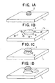
- Fig.1A, Fig.1B, Fig.1C and Fig.1D are diagrams schematically showing one embodiment of producing processes of a fine projection composite structure of the present invention.
- a fine metal particle 2 is disposed on a semiconductor substrate 1.
- a combination of a semiconductor and a metal which, from a thermodynamic point of view, forms a solid solution at an elevated temperature and separates at low temperature
- a Si substrate is employed as the semiconductor substrate 1
- Au, Ag, Al and the like can be employed.
- a Ge substrate is employed as a semiconductor substrate 1
- Zn, Cd, Au, Ag, Al can be employed.
- various combinations of semiconductors and metals which form solid solutions at an elevated temperature and separate at a low temperature, can be used.
- the surface of a semiconductor substrate 1 should be made sufficiently clean.
- the fine metal particle 2 is formed under decompression or vacuum state.
- the formation method of the fine metal particle 2 is not restricted to the particular one but a method capable of forming the fine metal particles 2 on the semiconductor substrate 1 held at room temperature can be employed. If a fine metal particle 2 is formed on a heated semiconductor substrate 1, it is likely that a reaction layer or the like is formed at the interface between the semiconductor substrate 1 and the fine metal particle 2 and is likely to adversely affect on the later processes.
- a gas phase condensation method of metal can be cited.
- the particle size of the fine metal particle 2 can be a size with which the fine metal particle can incorporate a semiconductor element (Si atoms, for instance) diffusing on the semiconductor substrate 1 during heat-treatment, resulting in formation of a semiconductor-metal solid solution.
- the diameter of the fine metal particle 2 is preferred to be 1 ⁇ m or less, more preferable to be 100nm or less.
- heat treatment is carried out at a temperature higher than that where a constituent element of the semiconductor substrate 1 can dissolve into the fine metal particle 2 to form a solid solution in a vacuum.
- a constituent element of the semiconductor substrate 1 can dissolve into the fine metal particle 2 to form a solid solution in a vacuum.
- a rapid diffusion of its constituent atoms la occurs on the surface of the semiconductor substrate 1.
- the diffusing atoms (semiconductor atoms) 1a are incorporated into the fine metal particle 2.
- a semiconductor-metal solid solution phase is formed.
- a homogeneous semiconductor-metal solid solution liquid phase that is, a semiconductor-metal liquid droplet 3 can be obtained.
- the heat-treatment temperature when the semiconductor substrate 1 and the fine metal particle 2 form an eutectic, is at least its eutectic temperature or more.
- a semiconductor-metal solid solution phase is preferred to be a liquid phase but can be a pseudo-liquid phase where semiconductor atoms and metal atoms are rapidly diffusing.
- a liquid droplet 3 consisting of a semiconductor-metal solid solution liquid phase
- this is annealed.
- constituent atoms of the semiconductor substrate 1 precipitate from within a semiconductor-metal droplet 3 to a solid-liquid interface between the liquid droplet 3 and the semiconductor substrate 1, and precipitate with an epitaxial relation with respect to the semiconductor substrate 1.
- Precipitation of the constituent atoms of the semiconductor substrate 1 are considered to base on the size effect of the semiconductor-metal liquid droplet 3, the heat treatment temperature, the cooling speed and so on. Though the cooling rate is different depending on constituent material, about 2K/min or less is preferable.
- the constituent atoms of the semiconductor substrate 1 gradually precipitate from the semiconductor-metal liquid droplet 3, and precipitate maintaining an epitaxial relation with respect to the semiconductor substrate 1, thus, a semiconductor layer 4' grows projectingly between the semiconductor-metal liquid droplet 3 and the semiconductor substrate 1. That is, the constituent atoms of the semiconductor substrate 1 grow due to liquid phase epitaxy from the semiconductor-metal liquid droplet 3. On the semiconductor substrate 1, a projection-like semiconductor layer 4' is gradually formed.
- a semiconductor fine projection 4 can be formed almost completely separated from metal matrix (metal fine particle 2). Besides, the fine metal particle 2 remains as a metal layer 5 at the upper portion of the semiconductor fine projection 4.
- a fine composite projection 5 of 2 layered structure which is composed of the semiconductor fine projection 4 possessing a selective and epitaxial relation, and a metal layer 2' disposed selectively on the semiconductor fine projection 4, can be formed.
- the semiconductor fine projection 4 and the metal layer 2' in the fine composite projection 5 can be completely separated.
- the shape of the semiconductor fine projection 4 since the semiconductor atoms grow through gradual precipitation from the semiconductor-metal liquid droplet 3, its cross-section becomes a projection like having a nearly trapezoid shape.
- the semiconductor fine projection 4 becomes a truncated cone shape, for instance.
- the semiconductor fine projection 4, depending on the initial size of the fine metal particle 2, can be made 1um or less in diameter at its maximum portion and about 50nm or more in diameter at its minimum portion.
- the size of the semiconductor fine projection 4 can be further reduced to 100nm or less in diameter at its maximum portion and 10nm in diameter at its minimum portion.
- the metal layer 2' can be made to have, for instance, the maximum diameter nearly equal to the diameter at the minimum portion of the semiconductor fine projection 4 and to have a cross-section of a nearly triangle shape possessing such the minimum diameter as 1nm or less.
- a fine composite projection 5 of a 2 layered structure which has a semiconductor fine projection 4 which is about 100nm or less (more preferably 50nm or less) in diameter at its maximum portion and is epitaxially grown selectively with respect to the semiconductor substrate 1, and a metal layer 2' which is disposed selectively on the semiconductor fine projection 4 and is nearly completely separated from the semiconductor fine projection 4, can be formed.
- a nanometer scale composite dot 5 having a hetero-junction interface composed of almost completely separated semiconductor/metal can be obtained.
- the size of the initial fine metal particle 2 is small such as 10nm or less, the metal layer 2' also grows epitaxially with respect to the semiconductor fine projection 4.
- the size of the semiconductor fine projection 4 can be controlled through the size of the initial fine metal particle 2 or the heat treatment temperature. Further, through control of the disposing position of the fine metal particle 2, the formation position of the semiconductor fine projection 4 can be controlled on the surface of the semiconductor substrate 1.
- a unit element size of, for example, nanometer scale can be made to be realized. It is remarkably effective for realizing an ultra-high integration semiconductor device or a quantum size device. Other than these, various kinds of fine devices can be materialized.
- a metal layer 2' can be removed.
- a semiconductor fine projection 4 the diameter of which at the maximum portion is 100nm or less (more preferably 50nm or less) and which is epitaxially grown selectively with respect to the semiconductor substrate 1, can be obtained.
- a fine projection consisting only of such a semiconductor fine projection 4 is also effective when realizing an ultra-high integration semiconductor or a quantum size device.
- the Si(111) single-crystal substrate is treated by chemical cleaning, to remove a native oxide layer and to obtain a hydrogen-terminated Si surface, the Si substrate was dipped in a diluted HF solution(2 weight %) for 30 seconds.
- pre-treated Si(111) single-crystal substrate was mounted in a vacuum chamber with a background pressure of less than 133 ⁇ Pa (1 ⁇ 10 -6 Torr).
- Au fine particles were deposited on the surface of the above described Si(111) single-crystal substrate.
- the Au fine particles were generated with a gas phase condensation method. That is, by evaporating Au of 99.99% purity in an Ar gas atmosphere, the Au fine particles were deposited on the Si(111) single-crystal substrate.
- Ar gas pressure was set at 800 Pa (6Torr) to obtain Au fine particles of about 10nm in diameter.
- These Au fine particles were deposited on the Si single-crystal substrate at room temperature. Diameter of the obtained Au fine particles was observed with a TEM and was found to be about 10 to 15nm.
- the Si single-crystal substrate deposited with the Au fine particles was heat-treated in a high vacuum chamber of less than 1.33 ⁇ Pa (1 ⁇ 10 -8 Torr).
- the temperature of the substrate is elevated at a rate of 15K/min up to 1073K and maintained at this temperature for 30min.
- the substrate was gradually cooled at a rate of -2K/min down to room temperature.
- Fig.3 is a diagram schematically illustrating a cross-sectional TEM image of the specimen after heat-treatment.
- TEM image was taken from ⁇ 110> direction of the Si single-crystal substrate.
- Fig.4, Fig.5 and Fig.6 show EDX spectra of each portions of the specimen after heat-treatment.
- Fig.4 is an EDX spectrum taken at the point A of Fig.3
- Fig.5 is an EDX spectrum taken at the point B of Fig.3
- Fig.6 is an EDX spectrum taken at the point C of Fig.3 . From the results obtained at the point A, as illustrated in the spectrum of Fig.4 , peaks of only Si are apparent. Thus, it is obvious that, even after the heat-treatment, the Si(111) single-crystal substrate 11 maintains its state.
- the lattice image of Si is clearly obtained at the lower portion 13 of the fine dot 12 of the 2 layered structure.
- this TEM image clearly shows that the lower portion (Si layer) 13 of the fine dot 12 maintains an identical crystal direction with respect to the Si(111) single-crystal substrate 11.
- the truncated cone-like shaped Si layer (Si dot) 13 of about 10nm in the minimum diameter has epitaxially grown with respect to the Si(111) single-crystal substrate 11 on the surface of the Si(111) single-crystal substrate 11.
- the fine dot 12 is confirmed to be constituted of a Si dot 13 grown epitaxially with respect to the Si(111) single-crystal substrate 11, and a Au layer 14 which is disposed on the Si dot 13 and is constituted of almost Au alone separated from the Si dot 13. That is, a Si-Au nanometer scale composite dot possessing an almost completely separated Si/Au interface was obtained.
- the above described Si-Au nanometer scale composite structure is considered to be formed through the following liquid phase epitaxy.
- Si atoms diffusing on the surface of the Si substrate are incorporated into the Au particles to form Si-Au liquid droplets. This is evident from that the heat treatment temperature is sufficiently higher than the eutectic temperature of Si-Au of 643K.
- Si atoms precipitate at the liquid-solid interface between Si-Au liquid droplet and Si, and, during cooling process, grow epitaxially on the Si substrate.
- Si dots are formed almost completely separated from Au fine particles, and Au layers remain on the Si dots.
- an epitaxial semiconductor dot or a semiconductor-metal composite dot of nanometer scale can be obtained. These remarkably contribute in realizing an ultra-high integration semiconductor device or a quantum-size device.
Landscapes
- Recrystallisation Techniques (AREA)
Description
- The present invention relates to a fine projection composite structure in which a fine projection such as a semiconductor dot or a semiconductor/metal composite dot both of nanometer scale is formed on a semiconductor substrate, and a fabricating method thereof.
- An integration rate of a semiconductor device represented by a DRAM is increasing year by year. For instance, the integration rate of a DRAM has been heightened from 16Mbit to 64Mbit or 256Mbit, and further development of a semiconductor device of the integration rate of more than Gbit is under way. Such a high integration of a semiconductor device has been achieved through reduction of a unit element size down to sub-micron order. For miniaturization of the unit size, development in lithography technology has largely contributed. In addition to improvement of lithography technology, improvement of an element structure is also in progress.
- Concerning the lithography technology, due to improvement of i-line exposure technique and positive photoresist, 0.5µm rule corresponding to 16Mbit-DRAM is being put into practical use. Further, due to development of the exposure technique using KrF excimer laser which can correspond to 0.25 µm rule, 64Mbit-DRAM is being mass produced and the practical use of 256Mbit-DRAM is under way. Further, correspondence to 0.18µm rule due to improvement of the exposure technique employing KrF excimer laser or development of the exposure technique employing the SOR light is under way. However, the limit of present lithography technology is considered to be about 0.1µm rule. Therefore, in order to achieve further higher integration, it is desired to be realized in the future a unit element size of nanometer scale.
- Further, a quantum-size device is attracting attention as a candidate of future LSI technology. Realization of a new device utilizing a quantum-size effect or a tunnel effect, for example, such as a quantum wire device or a quantum dot device which makes use of a wire or a dot structure of which sectional dimension is at the same degree with a quantum mechanical wavelength of an electron, a resonant tunnelling effect device or a resonant tunnelling element utilizing a quantum well and so on, are being tried.
- In order to develop a new device which positively utilizes a quantum effect, a characteristic dimension of an element should not remain in a phase wavelength (0.1 to 1µm) order, namely in a mesoscopic region, but should be brought into an electron wavelength order (10 to 100nm), namely in a microscopic region. Further, in order to utilize more effectively a quantum effect device, ultra-miniaturization of the unit element size itself of, for instance, 10 to 100 nm, more preferably less than 10 nm is required. However it is far beyond the present lithography technology level.
- As described above, research and development of the quantum size device and the like which are expected as candidates of a ultra-high integration semiconductor device or future LSI technology are under way. To materialize such a fine device, a unit element size of nanometer scale is required to be achieved. Therefore a technology enabling to obtain with reproducibility a semiconductor dot or a semiconductor/metal composite dot, which is necessary for an ultra-high integration semiconductor device or a quantum-size device, is desired to be developed.
-
US 5 544 617 describes a method of producing a single needle like crystal in an SiH4 or SiCl4 atmosphere. - Givargizov "Ultrasharp tips for field emission applications prepared by the vapor-liquid-solid growth technique" in J. Vac. Sci. Technol. ) describes the manufacture of Si whiskers in an SiCl4+H2 gas.
-
EP 0 838 865 which forms the state of the art under article 54(3) describes a method of forming quantum wires in a Silane gas atmosphere. - An object of the present invention is to provide a fine projection structure of nanometer scale, which enables to realize a high integration semiconductor device or a quantum size device, and fabricating method thereof.
- The present invention provides a manufacturing method as defined in
Claim 1. - With the benefit of the present invention, a heat treatment can be given to a semiconductor substrate being disposed with fine metal particles, at first, at a temperature where a constituent element of the semiconductor substrate is incorporated into the fine metal particles to form a solid solution in a vacuum atmosphere, further at a temperature equal or more than that where the constituent element of the semiconductor substrate and the fine metal particles dissolve to form a homogeneous liquid solid solution phase. By cooling from this liquid solid solution state, the constituent element of the semiconductor substrate can be precipitated from the liquid solid solution phase.
- Through precipitation from such a liquid phase, the constituent element of the semiconductor substrate grows epitaxially with respect to the semiconductor substrate. Further, the constituent element of the semiconductor substrate and the fine metal particle separate. Therefore, according to the size and the position of the initial fine particles, semiconductor fine projections can be formed epitaxially with respect to the semiconductor substrate. In addition, even after the constituent element of the semiconductor substrate is precipitated, the fine metal particles remain on the semiconductor fine projections as metal layers. Therefore, a fine composite structure having a hetero-junction interface between a semiconductor layer having a projection shape (semiconductor fine projection) and a metal layer can be obtained.
- The shape of a semiconductor fine projection can be, for example, a trapezoid-like shape or variation thereof.
The fine projection of the trapezoid-like shape or modification thereof can be reduced to 1µm or less in diameter at the maximum portion thereof, more preferably to 100nm or less. The fine projection of the trapezoid-like shape or modification thereof can be made to 50nm or less in diameter at the minimum portion thereof, more preferably to 10nm or less. The size of the metal layer existing at the upper portion of semiconductor fine projection can be made nearly identical. Further, through elimination of the metal layer at the upper portion, only a semiconductor fine projection can be obtained. According to such a fine projection, a unit element size of nanometer scale, which is required in, for example, a ultra-high integration semiconductor device or a quantum-size device, can be realized. -
Fig.1A, Fig.1B, Fig.1C and Fig.1D are diagrams schematically showing one embodiment of fabricating processes of a fine projection composite structure of the present invention and a fine projection composite structure obtained thereby. -
Fig.2 is a diagram schematically showing a structure of another fine projection composite structure of the present invention. -
Fig.3 is a diagram schematically showing TEM observation results of a fine projection composite structure fabricated inembodiment 1 of the present invention. -
Fig.4 is a diagram showing a result of an EDX analysis of A portion of the fine projection composite structure shown inFig.3 . -
Fig.5 is a diagram showing a result of an EDX analysis of B portion of the fine projection composite structure shown inFig.3 . -
Fig.6 is a diagram showing a result of an EDX analysis of B portion of the fine projection composite structure shown inFig.3 . - In the following, embodiments carrying out the present invention will be described with reference to the drawings.
-
Fig.1A, Fig.1B, Fig.1C and Fig.1D are diagrams schematically showing one embodiment of producing processes of a fine projection composite structure of the present invention. At first, as shown inFig.1A , afine metal particle 2 is disposed on asemiconductor substrate 1. - As a
semiconductor substrate 1 and a fine metal particle, a combination of a semiconductor and a metal, which, from a thermodynamic point of view, forms a solid solution at an elevated temperature and separates at low temperature, can be employed. When a Si substrate is employed as thesemiconductor substrate 1, for instance, as a constituent member of thefine metal particle 2, Au, Ag, Al and the like can be employed. In addition, when a Ge substrate is employed as asemiconductor substrate 1, as a constituent member of thefine metal particle 2, Zn, Cd, Au, Ag, Al can be employed. Like this, various combinations of semiconductors and metals, which form solid solutions at an elevated temperature and separate at a low temperature, can be used. - When forming a
fine metal particle 2, the surface of asemiconductor substrate 1 should be made sufficiently clean. On the surface of such asemiconductor substrate 1, thefine metal particle 2 is formed under decompression or vacuum state. The formation method of thefine metal particle 2 is not restricted to the particular one but a method capable of forming thefine metal particles 2 on thesemiconductor substrate 1 held at room temperature can be employed. If afine metal particle 2 is formed on aheated semiconductor substrate 1, it is likely that a reaction layer or the like is formed at the interface between thesemiconductor substrate 1 and thefine metal particle 2 and is likely to adversely affect on the later processes. As a method formingfine metal particles 2, a gas phase condensation method of metal can be cited. - The particle size of the
fine metal particle 2, as will be described later, can be a size with which the fine metal particle can incorporate a semiconductor element (Si atoms, for instance) diffusing on thesemiconductor substrate 1 during heat-treatment, resulting in formation of a semiconductor-metal solid solution. To be specific, the diameter of thefine metal particle 2 is preferred to be 1µm or less, more preferable to be 100nm or less. When an initial particle size of thefine metal particle 2 is too large, during formation process or heat treatment process thereof, it is likely that a reaction layer or the like is formed at the interface between thesemiconductor substrate 1 and thefine metal particle 2. The interface reaction layer tends to adversely affect on the later processes and to disturb the precipitation of the semiconductor atoms from the semiconductor-metal solid solution phase. - Next, to the
semiconductor substrate 1 disposed with thefine metal particles 2, heat treatment is carried out at a temperature higher than that where a constituent element of thesemiconductor substrate 1 can dissolve into thefine metal particle 2 to form a solid solution in a vacuum. As illustrated inFig.1B , when the semiconductor substrate disposed with thefine metal particle 2 is heat treated in a vacuum, during the temperature elevating process, a rapid diffusion of its constituent atoms la occurs on the surface of thesemiconductor substrate 1. The diffusing atoms (semiconductor atoms) 1a are incorporated into thefine metal particle 2. Thus, a semiconductor-metal solid solution phase is formed. - In particular, by carrying out the heat treatment at a temperature higher than that where a liquid phase, in which the
fine metal particle 2 and the semiconductor atoms la are homogeneously dissolved, can be formed, a homogeneous semiconductor-metal solid solution liquid phase, that is, a semiconductor-metal liquid droplet 3 can be obtained. The heat-treatment temperature, when thesemiconductor substrate 1 and thefine metal particle 2 form an eutectic, is at least its eutectic temperature or more. Anyway, it can be a temperature higher than or equal to that where a semiconductor-metal liquid droplet 3 can be formed. Here, a semiconductor-metal solid solution phase is preferred to be a liquid phase but can be a pseudo-liquid phase where semiconductor atoms and metal atoms are rapidly diffusing. - After formation of a
liquid droplet 3 consisting of a semiconductor-metal solid solution liquid phase, this is annealed. As illustrated in Fig.lC, during annealing, constituent atoms of thesemiconductor substrate 1 precipitate from within a semiconductor-metal droplet 3 to a solid-liquid interface between theliquid droplet 3 and thesemiconductor substrate 1, and precipitate with an epitaxial relation with respect to thesemiconductor substrate 1. Precipitation of the constituent atoms of thesemiconductor substrate 1 are considered to base on the size effect of the semiconductor-metal liquid droplet 3, the heat treatment temperature, the cooling speed and so on. Though the cooling rate is different depending on constituent material, about 2K/min or less is preferable. - As described above, the constituent atoms of the
semiconductor substrate 1 gradually precipitate from the semiconductor-metal liquid droplet 3, and precipitate maintaining an epitaxial relation with respect to thesemiconductor substrate 1, thus, a semiconductor layer 4' grows projectingly between the semiconductor-metal liquid droplet 3 and thesemiconductor substrate 1. That is, the constituent atoms of thesemiconductor substrate 1 grow due to liquid phase epitaxy from the semiconductor-metal liquid droplet 3. On thesemiconductor substrate 1, a projection-like semiconductor layer 4' is gradually formed. - And, by completing the precipitation of the semiconductor atoms from the semiconductor-
metal liquid droplet 3 within the cooling process, as illustrated in Fig.lD, a semiconductorfine projection 4 can be formed almost completely separated from metal matrix (metal fine particle 2). Besides, thefine metal particle 2 remains as ametal layer 5 at the upper portion of the semiconductorfine projection 4. Thus, on the surface of thesemiconductor substrate 1, a finecomposite projection 5 of 2 layered structure, which is composed of the semiconductorfine projection 4 possessing a selective and epitaxial relation, and a metal layer 2' disposed selectively on the semiconductorfine projection 4, can be formed. - The semiconductor
fine projection 4 and the metal layer 2' in the finecomposite projection 5 can be completely separated. The shape of the semiconductorfine projection 4, since the semiconductor atoms grow through gradual precipitation from the semiconductor-metal liquid droplet 3, its cross-section becomes a projection like having a nearly trapezoid shape. The semiconductorfine projection 4 becomes a truncated cone shape, for instance. The semiconductorfine projection 4, depending on the initial size of thefine metal particle 2, can be made 1um or less in diameter at its maximum portion and about 50nm or more in diameter at its minimum portion. The size of the semiconductorfine projection 4 can be further reduced to 100nm or less in diameter at its maximum portion and 10nm in diameter at its minimum portion. The metal layer 2' can be made to have, for instance, the maximum diameter nearly equal to the diameter at the minimum portion of the semiconductorfine projection 4 and to have a cross-section of a nearly triangle shape possessing such the minimum diameter as 1nm or less. - Thus, by applying a fabricating method of the present invention, on an arbitrary position of a
semiconductor substrate 1, a finecomposite projection 5 of a 2 layered structure, which has a semiconductorfine projection 4 which is about 100nm or less (more preferably 50nm or less) in diameter at its maximum portion and is epitaxially grown selectively with respect to thesemiconductor substrate 1, and a metal layer 2' which is disposed selectively on the semiconductorfine projection 4 and is nearly completely separated from the semiconductorfine projection 4, can be formed. In other words, a nanometer scalecomposite dot 5 having a hetero-junction interface composed of almost completely separated semiconductor/metal can be obtained. When the size of the initialfine metal particle 2 is small such as 10nm or less, the metal layer 2' also grows epitaxially with respect to the semiconductorfine projection 4. - The size of the semiconductor
fine projection 4 can be controlled through the size of the initialfine metal particle 2 or the heat treatment temperature. Further, through control of the disposing position of thefine metal particle 2, the formation position of the semiconductorfine projection 4 can be controlled on the surface of thesemiconductor substrate 1. Through the use of such a finecomposite projection 5 of the 2 layered structure, a unit element size of, for example, nanometer scale can be made to be realized. It is remarkably effective for realizing an ultra-high integration semiconductor device or a quantum size device. Other than these, various kinds of fine devices can be materialized. - When only a semiconductor
fine projection 4 is necessary, a metal layer 2' can be removed. By undergoing such a process, as illustrated inFig.2 , on an arbitrary position of the surface of thesemiconductor substrate 1, a semiconductorfine projection 4, the diameter of which at the maximum portion is 100nm or less (more preferably 50nm or less) and which is epitaxially grown selectively with respect to thesemiconductor substrate 1, can be obtained. A fine projection consisting only of such a semiconductorfine projection 4 is also effective when realizing an ultra-high integration semiconductor or a quantum size device. - In the following, concrete embodiments of the present invention will be described.
- At first, a Si(111) single-crystal substrate (non-doped, a0=0.5431nm) is prepared. After the Si(111) single-crystal substrate is treated by chemical cleaning, to remove a native oxide layer and to obtain a hydrogen-terminated Si surface, the Si substrate was dipped in a diluted HF solution(2 weight %) for 30 seconds. Following, pre-treated Si(111) single-crystal substrate was mounted in a vacuum chamber with a background pressure of less than 133 µPa (1×10⁻⁶Torr).
- Then, on the surface of the above described Si(111) single-crystal substrate, Au fine particles were deposited. The Au fine particles were generated with a gas phase condensation method. That is, by evaporating Au of 99.99% purity in an Ar gas atmosphere, the Au fine particles were deposited on the Si(111) single-crystal substrate. Ar gas pressure was set at 800 Pa (6Torr) to obtain Au fine particles of about 10nm in diameter. These Au fine particles were deposited on the Si single-crystal substrate at room temperature. Diameter of the obtained Au fine particles was observed with a TEM and was found to be about 10 to 15nm.
- Next, the Si single-crystal substrate deposited with the Au fine particles was heat-treated in a high vacuum chamber of less than 1.33 µPa (1 × 10⁻⁸Torr). The temperature of the substrate is elevated at a rate of 15K/min up to 1073K and maintained at this temperature for 30min. Then, the substrate was gradually cooled at a rate of -2K/min down to room temperature.
- The structure and the composition of the above described heat treated specimen were evaluated with a high resolution transmission electron microscope (HRTEM, JEOL-2010) and an energy dispersive X-ray spectrometer (EDX, Oxford-Link ISIS). These results are shown in
Fig.3 ,Fig.4 ,Fig.5 and Fig.6 .Fig.3 is a diagram schematically illustrating a cross-sectional TEM image of the specimen after heat-treatment. TEM image was taken from <110> direction of the Si single-crystal substrate.Fig.4, Fig.5 and Fig.6 show EDX spectra of each portions of the specimen after heat-treatment. - From a schematized diagram of a cross-sectional TEM image illustrated in
Fig.3 , it is obvious that, on the surface of the Si single-crystal substrate 11, a fine dot of a 2 layered structure is formed. In thefine dot 12 of the 2 layered structure, thelower layer portion 13 possesses a truncated cone-like shape, the diameter of its minimum portion was about 10nm, and that of the maximum portion was about 30nm. Theupper portion 14 possesses the maximum diameter of about 15nm and a projection like shape of which the minimum diameter at the tip portion is 1nm or less. Here, in order to evaluate the compositions of each layers 11, 13, 14, EDX spectra were obtained. The EDX analysis was carried out with an electron beam of a diameter converged to less than 5nm. The evaluated positions are shown inFig.3 as point A, point B and point C. -
Fig.4 is an EDX spectrum taken at the point A ofFig.3 ,Fig.5 is an EDX spectrum taken at the point B ofFig.3 ,Fig.6 is an EDX spectrum taken at the point C ofFig.3 . From the results obtained at the point A, as illustrated in the spectrum ofFig.4 , peaks of only Si are apparent. Thus, it is obvious that, even after the heat-treatment, the Si(111) single-crystal substrate 11 maintains its state. - From the results obtained at the point B, as shown in the spectrum of
Fig.5 , it is obvious that the lower portion (neck portion) 13 of afine dot 12 of a 2 layered structure is formed of only Si. In addition, since the peak of Au in the spectrum ofFig.5 is in the range of error, this layer can be regarded as a Si single crystal layer. - Actually, in the TEM image schematically illustrated in
Fig.3 , the lattice image of Si is clearly obtained at thelower portion 13 of thefine dot 12 of the 2 layered structure. In addition, this TEM image clearly shows that the lower portion (Si layer) 13 of thefine dot 12 maintains an identical crystal direction with respect to the Si(111) single-crystal substrate 11. Thus, the truncated cone-like shaped Si layer (Si dot) 13 of about 10nm in the minimum diameter has epitaxially grown with respect to the Si(111) single-crystal substrate 11 on the surface of the Si(111) single-crystal substrate 11. - Further, from the results obtained at the point C, as shown in
Fig.6 , in theupper portion 14 of thefine dot 12 of the 2 layered structure, it is found that Au is a dominant component, though trivial Si being found. - Thus, the
fine dot 12 is confirmed to be constituted of aSi dot 13 grown epitaxially with respect to the Si(111) single-crystal substrate 11, and aAu layer 14 which is disposed on theSi dot 13 and is constituted of almost Au alone separated from theSi dot 13. That is, a Si-Au nanometer scale composite dot possessing an almost completely separated Si/Au interface was obtained. - The above described Si-Au nanometer scale composite structure is considered to be formed through the following liquid phase epitaxy. At first, by carrying out the heat treatment in a high vacuum with respect to the Si substrate deposited with Au fine particles, Si atoms diffusing on the surface of the Si substrate are incorporated into the Au particles to form Si-Au liquid droplets. This is evident from that the heat treatment temperature is sufficiently higher than the eutectic temperature of Si-Au of 643K.
- By annealing after formation of the liquid droplets obtained by mixing Si and Au in liquid phase, Si atoms precipitate at the liquid-solid interface between Si-Au liquid droplet and Si, and, during cooling process, grow epitaxially on the Si substrate. By completing such precipitation of Si in the course of the cooling process, Si dots are formed almost completely separated from Au fine particles, and Au layers remain on the Si dots.
- Further, when the
Au layer 14 of the upper portion in the above described Si-Au nanometer scalecomposite dot 12 is removed, only Si dot 13 which is epitaxially grown with respect to the Si(111) single-crystal substrate 11 was obtained. - As evident from the above described embodiments, according to the present invention, an epitaxial semiconductor dot or a semiconductor-metal composite dot of nanometer scale can be obtained. These remarkably contribute in realizing an ultra-high integration semiconductor device or a quantum-size device.
Claims (7)
- A manufacturing method of a fine projection composite structure, comprising the following steps of:disposing a fine metal particle on a semiconductor substrate;heat treating in a vacuum the semiconductor substrate provided with the fine metal particle at a temperature higher than or equal to that where the constituent element of the semiconductor substrate dissolve into the fine metal particle to form a liquid solid solution phase including the constituent element of the semiconductor substrate and the constituent element of the fine metal particle homogeneously; andannealing in a vacuum the liquid solid solution phase for growing a semiconductor fine projection consisting essentially of the constituent element of the semiconductor substrate and having an epitaxial relation with respect to the semiconductor substrate by precipitating the constituent element of the semiconductor substrate from the liquid phase; characterised bycompleting precipitation of the semiconductor atoms from the semiconductor-metal liquid within a cooling process which cools gradually the liquid phase from the heat treating temperature to room temperature at a cooling rate of 2 K/min or less to form the fine projection composite structure having the semiconductor fine projection completely separated from the metal particle which remains as a metal layer at the upper portion of the semiconductor fine projection.
- A manufacturing method of a fine projection composite structure as set forth in claim 1:wherein the fine metal particle is 1µm or less in diameter.
- A manufacturing method of a fine projection composite structure as set forth in claims 1 or 2:wherein the fine metal particle is formed on the semiconductor substrate maintained at room temperature.
- A manufacturing method of a fine projection composite structure as set forth in any preceding claim, further comprising the step of:removing the metal layer on the semiconductor fine projection.
- A manufacturing method of a fine projection composite structure as set forth in any preceding claim,
wherein the semiconductor substrate contains Si, and the fine metal particle consists essentially of at least one selected from Au, Ag and Al. - A manufacturing method of a fine projection composite structure as set forth in any preceding claim,
wherein the semiconductor fine projection has a trapezoid-like shape in its cross section, and the maximum diameter of the trapezoid-like shape is 1µm or less, and the minimum diameter of the trapezoid-like shape is 50nm or less. - A manufacturing method of a fine projection composite structure as set forth in any preceding claim,
wherein the heat treating step and the annealing step are taken in the vacuum atmosphere of less than 1.33×10⁻⁶ Pa (1 x 10⁻⁸ Torr.)
Applications Claiming Priority (3)
| Application Number | Priority Date | Filing Date | Title |
|---|---|---|---|
| JP153651/97 | 1997-06-11 | ||
| JP15365197A JP3452764B2 (en) | 1997-06-11 | 1997-06-11 | Method for manufacturing ultrafine projection structure |
| JP15365197 | 1997-06-11 |
Publications (3)
| Publication Number | Publication Date |
|---|---|
| EP0884768A2 EP0884768A2 (en) | 1998-12-16 |
| EP0884768A3 EP0884768A3 (en) | 2000-01-05 |
| EP0884768B1 true EP0884768B1 (en) | 2010-01-06 |
Family
ID=15567208
Family Applications (1)
| Application Number | Title | Priority Date | Filing Date |
|---|---|---|---|
| EP98304603A Expired - Lifetime EP0884768B1 (en) | 1997-06-11 | 1998-06-10 | Fine structure and fabricating method thereof |
Country Status (4)
| Country | Link |
|---|---|
| US (1) | US6025604A (en) |
| EP (1) | EP0884768B1 (en) |
| JP (1) | JP3452764B2 (en) |
| DE (1) | DE69841429D1 (en) |
Families Citing this family (4)
| Publication number | Priority date | Publication date | Assignee | Title |
|---|---|---|---|---|
| US6653653B2 (en) | 2001-07-13 | 2003-11-25 | Quantum Logic Devices, Inc. | Single-electron transistors and fabrication methods in which a projecting feature defines spacing between electrodes |
| US6483125B1 (en) * | 2001-07-13 | 2002-11-19 | North Carolina State University | Single electron transistors in which the thickness of an insulating layer defines spacing between electrodes |
| JP4673070B2 (en) * | 2005-01-20 | 2011-04-20 | 日本電信電話株式会社 | Microstructure growth control method |
| KR100849418B1 (en) | 2007-05-10 | 2008-08-01 | 한양대학교 산학협력단 | Cobalt Piti Nanoparticles Formation Method |
Family Cites Families (5)
| Publication number | Priority date | Publication date | Assignee | Title |
|---|---|---|---|---|
| US5006914A (en) * | 1988-12-02 | 1991-04-09 | Advanced Technology Materials, Inc. | Single crystal semiconductor substrate articles and semiconductor devices comprising same |
| JP2821061B2 (en) * | 1992-05-22 | 1998-11-05 | 電気化学工業株式会社 | Single crystal manufacturing method |
| US5828076A (en) * | 1994-04-19 | 1998-10-27 | Siemens Aktiengesellschaft | Microelectronic component and process for its production |
| JPH09132500A (en) * | 1995-11-10 | 1997-05-20 | Sony Corp | Trigonal pyramidal semiconductor structure and optical element using the same |
| US5976957A (en) * | 1996-10-28 | 1999-11-02 | Sony Corporation | Method of making silicon quantum wires on a substrate |
-
1997
- 1997-06-11 JP JP15365197A patent/JP3452764B2/en not_active Expired - Fee Related
-
1998
- 1998-06-09 US US09/094,031 patent/US6025604A/en not_active Expired - Lifetime
- 1998-06-10 DE DE69841429T patent/DE69841429D1/en not_active Expired - Lifetime
- 1998-06-10 EP EP98304603A patent/EP0884768B1/en not_active Expired - Lifetime
Non-Patent Citations (1)
| Title |
|---|
| E. I. GIVARGIZOV: "Fundamental Aspects of VLS Growth", JOURNAL OF CRYSTAL GROWTH, vol. 31, 18 August 1975 (1975-08-18), Amsterdam, The Netherlands, pages 20 - 30, XP001073851 * |
Also Published As
| Publication number | Publication date |
|---|---|
| EP0884768A2 (en) | 1998-12-16 |
| JPH113988A (en) | 1999-01-06 |
| DE69841429D1 (en) | 2010-02-25 |
| JP3452764B2 (en) | 2003-09-29 |
| EP0884768A3 (en) | 2000-01-05 |
| US6025604A (en) | 2000-02-15 |
Similar Documents
| Publication | Publication Date | Title |
|---|---|---|
| EP1613549B1 (en) | Precisely positioned nanowhisker structures and method for preparing them | |
| US7911035B2 (en) | Directionally controlled growth of nanowhiskers | |
| US6773616B1 (en) | Formation of nanoscale wires | |
| US7960260B2 (en) | Formation of nanowhiskers on a substrate of dissimilar material | |
| US20090197416A1 (en) | Silicon nano wire having a silicon-nitride shell and mthod of manufacturing the same | |
| US6242326B1 (en) | Method for fabricating compound semiconductor substrate having quantum dot array structure | |
| Han et al. | Controlled growth of gallium nitride single-crystal nanowires using a chemical vapor deposition method | |
| JP2821061B2 (en) | Single crystal manufacturing method | |
| US20100065810A1 (en) | Method Of Synthesizing Semiconductor Nanostructures And Nanostructures Synthesized By The Method | |
| US7229498B2 (en) | Nanostructures produced by phase-separation during growth of (III-V)1-x(IV2)x alloys | |
| US9647063B2 (en) | Nanoscale chemical templating with oxygen reactive materials | |
| US6033972A (en) | Growing method of GaAs quantum dots using chemical beam epitaxy | |
| US6025604A (en) | Fine projection structure and fabricating method thereof | |
| CN100405552C (en) | electron beam micromachining method | |
| WO2008035662A1 (en) | Diamond electron source and method for manufacturing the same | |
| JPH0778807A (en) | Mask, method for forming the same, and etching method using the same | |
| JP3532431B2 (en) | Method for manufacturing structure for fine semiconductor element | |
| Wakayama et al. | Self-assembled nanocomposite structure of SiAu system formed by liquid phase epitaxy | |
| Wang et al. | Cu/SiO 2− x nanowires with compositional modulation structure grown via thermal evaporation | |
| EP1041611B1 (en) | Method of production of fine protuberance structure | |
| Hobart et al. | Growth of low-dimensional structures on nonplanar patterned substrates | |
| Zhang | Self-assembled nanostructures of group IV elements on germanium substrate by molecular beam epitaxy | |
| Wakayama et al. | Surface Droplet Epitaxy for Fabrication of Metal/Semiconductor Bilayer Dots on Nanometer Scale | |
| JP2006108440A (en) | Semiconductor device and manufacturing method thereof | |
| Hobart et al. | Atomically sharp features grown by silicon molecular beam epitaxy |
Legal Events
| Date | Code | Title | Description |
|---|---|---|---|
| PUAI | Public reference made under article 153(3) epc to a published international application that has entered the european phase |
Free format text: ORIGINAL CODE: 0009012 |
|
| 17P | Request for examination filed |
Effective date: 19980709 |
|
| AK | Designated contracting states |
Kind code of ref document: A2 Designated state(s): DE FR GB |
|
| AX | Request for extension of the european patent |
Free format text: AL;LT;LV;MK;RO;SI |
|
| PUAL | Search report despatched |
Free format text: ORIGINAL CODE: 0009013 |
|
| RIC1 | Information provided on ipc code assigned before grant |
Free format text: 6H 01L 21/20 A, 6H 01L 29/12 B, 6C 30B 19/00 B, 6C 30B 1/00 B |
|
| AK | Designated contracting states |
Kind code of ref document: A3 Designated state(s): AT BE CH CY DE DK ES FI FR GB GR IE IT LI LU MC NL PT SE |
|
| AX | Request for extension of the european patent |
Free format text: AL;LT;LV;MK;RO;SI |
|
| RAP1 | Party data changed (applicant data changed or rights of an application transferred) |
Owner name: KABUSHIKI KAISHA TOSHIBA Owner name: JAPAN SCIENCE AND TECHNOLOGY CORPORATION |
|
| AKX | Designation fees paid |
Free format text: DE FR GB |
|
| 17Q | First examination report despatched |
Effective date: 20020823 |
|
| 17Q | First examination report despatched |
Effective date: 20020823 |
|
| GRAP | Despatch of communication of intention to grant a patent |
Free format text: ORIGINAL CODE: EPIDOSNIGR1 |
|
| GRAS | Grant fee paid |
Free format text: ORIGINAL CODE: EPIDOSNIGR3 |
|
| GRAA | (expected) grant |
Free format text: ORIGINAL CODE: 0009210 |
|
| RAP1 | Party data changed (applicant data changed or rights of an application transferred) |
Owner name: JAPAN SCIENCE AND TECHNOLOGY AGENCY |
|
| AK | Designated contracting states |
Kind code of ref document: B1 Designated state(s): DE FR GB |
|
| REG | Reference to a national code |
Ref country code: GB Ref legal event code: FG4D |
|
| REF | Corresponds to: |
Ref document number: 69841429 Country of ref document: DE Date of ref document: 20100225 Kind code of ref document: P |
|
| PLBE | No opposition filed within time limit |
Free format text: ORIGINAL CODE: 0009261 |
|
| STAA | Information on the status of an ep patent application or granted ep patent |
Free format text: STATUS: NO OPPOSITION FILED WITHIN TIME LIMIT |
|
| 26N | No opposition filed |
Effective date: 20101007 |
|
| PGFP | Annual fee paid to national office [announced via postgrant information from national office to epo] |
Ref country code: DE Payment date: 20120622 Year of fee payment: 15 |
|
| PGFP | Annual fee paid to national office [announced via postgrant information from national office to epo] |
Ref country code: FR Payment date: 20120705 Year of fee payment: 15 Ref country code: GB Payment date: 20120622 Year of fee payment: 15 |
|
| GBPC | Gb: european patent ceased through non-payment of renewal fee |
Effective date: 20130610 |
|
| REG | Reference to a national code |
Ref country code: DE Ref legal event code: R119 Ref document number: 69841429 Country of ref document: DE Effective date: 20140101 |
|
| REG | Reference to a national code |
Ref country code: FR Ref legal event code: ST Effective date: 20140228 |
|
| PG25 | Lapsed in a contracting state [announced via postgrant information from national office to epo] |
Ref country code: DE Free format text: LAPSE BECAUSE OF NON-PAYMENT OF DUE FEES Effective date: 20140101 Ref country code: GB Free format text: LAPSE BECAUSE OF NON-PAYMENT OF DUE FEES Effective date: 20130610 |
|
| PG25 | Lapsed in a contracting state [announced via postgrant information from national office to epo] |
Ref country code: FR Free format text: LAPSE BECAUSE OF NON-PAYMENT OF DUE FEES Effective date: 20130701 |