US6033972A - Growing method of GaAs quantum dots using chemical beam epitaxy - Google Patents
Growing method of GaAs quantum dots using chemical beam epitaxy Download PDFInfo
- Publication number
- US6033972A US6033972A US09/135,124 US13512498A US6033972A US 6033972 A US6033972 A US 6033972A US 13512498 A US13512498 A US 13512498A US 6033972 A US6033972 A US 6033972A
- Authority
- US
- United States
- Prior art keywords
- droplets
- gaas
- tega
- quantum dots
- substrate
- Prior art date
- Legal status (The legal status is an assumption and is not a legal conclusion. Google has not performed a legal analysis and makes no representation as to the accuracy of the status listed.)
- Expired - Lifetime
Links
Images


Classifications
-
- H—ELECTRICITY
- H01—ELECTRIC ELEMENTS
- H01L—SEMICONDUCTOR DEVICES NOT COVERED BY CLASS H10
- H01L21/00—Processes or apparatus adapted for the manufacture or treatment of semiconductor or solid state devices or of parts thereof
- H01L21/02—Manufacture or treatment of semiconductor devices or of parts thereof
- H01L21/04—Manufacture or treatment of semiconductor devices or of parts thereof the devices having at least one potential-jump barrier or surface barrier, e.g. PN junction, depletion layer or carrier concentration layer
- H01L21/18—Manufacture or treatment of semiconductor devices or of parts thereof the devices having at least one potential-jump barrier or surface barrier, e.g. PN junction, depletion layer or carrier concentration layer the devices having semiconductor bodies comprising elements of Group IV of the Periodic System or AIIIBV compounds with or without impurities, e.g. doping materials
- H01L21/20—Deposition of semiconductor materials on a substrate, e.g. epitaxial growth solid phase epitaxy
-
- H—ELECTRICITY
- H01—ELECTRIC ELEMENTS
- H01L—SEMICONDUCTOR DEVICES NOT COVERED BY CLASS H10
- H01L21/00—Processes or apparatus adapted for the manufacture or treatment of semiconductor or solid state devices or of parts thereof
- H01L21/02—Manufacture or treatment of semiconductor devices or of parts thereof
- H01L21/02104—Forming layers
- H01L21/02365—Forming inorganic semiconducting materials on a substrate
- H01L21/02367—Substrates
- H01L21/0237—Materials
- H01L21/02387—Group 13/15 materials
- H01L21/02395—Arsenides
-
- B—PERFORMING OPERATIONS; TRANSPORTING
- B82—NANOTECHNOLOGY
- B82Y—SPECIFIC USES OR APPLICATIONS OF NANOSTRUCTURES; MEASUREMENT OR ANALYSIS OF NANOSTRUCTURES; MANUFACTURE OR TREATMENT OF NANOSTRUCTURES
- B82Y10/00—Nanotechnology for information processing, storage or transmission, e.g. quantum computing or single electron logic
-
- B—PERFORMING OPERATIONS; TRANSPORTING
- B82—NANOTECHNOLOGY
- B82Y—SPECIFIC USES OR APPLICATIONS OF NANOSTRUCTURES; MEASUREMENT OR ANALYSIS OF NANOSTRUCTURES; MANUFACTURE OR TREATMENT OF NANOSTRUCTURES
- B82Y30/00—Nanotechnology for materials or surface science, e.g. nanocomposites
-
- H—ELECTRICITY
- H01—ELECTRIC ELEMENTS
- H01L—SEMICONDUCTOR DEVICES NOT COVERED BY CLASS H10
- H01L21/00—Processes or apparatus adapted for the manufacture or treatment of semiconductor or solid state devices or of parts thereof
- H01L21/02—Manufacture or treatment of semiconductor devices or of parts thereof
- H01L21/02104—Forming layers
- H01L21/02365—Forming inorganic semiconducting materials on a substrate
- H01L21/02436—Intermediate layers between substrates and deposited layers
- H01L21/02439—Materials
- H01L21/02455—Group 13/15 materials
- H01L21/02463—Arsenides
-
- H—ELECTRICITY
- H01—ELECTRIC ELEMENTS
- H01L—SEMICONDUCTOR DEVICES NOT COVERED BY CLASS H10
- H01L21/00—Processes or apparatus adapted for the manufacture or treatment of semiconductor or solid state devices or of parts thereof
- H01L21/02—Manufacture or treatment of semiconductor devices or of parts thereof
- H01L21/02104—Forming layers
- H01L21/02365—Forming inorganic semiconducting materials on a substrate
- H01L21/02436—Intermediate layers between substrates and deposited layers
- H01L21/02494—Structure
- H01L21/02496—Layer structure
- H01L21/02502—Layer structure consisting of two layers
-
- H—ELECTRICITY
- H01—ELECTRIC ELEMENTS
- H01L—SEMICONDUCTOR DEVICES NOT COVERED BY CLASS H10
- H01L21/00—Processes or apparatus adapted for the manufacture or treatment of semiconductor or solid state devices or of parts thereof
- H01L21/02—Manufacture or treatment of semiconductor devices or of parts thereof
- H01L21/02104—Forming layers
- H01L21/02365—Forming inorganic semiconducting materials on a substrate
- H01L21/02518—Deposited layers
- H01L21/02521—Materials
- H01L21/02538—Group 13/15 materials
- H01L21/02546—Arsenides
-
- H—ELECTRICITY
- H01—ELECTRIC ELEMENTS
- H01L—SEMICONDUCTOR DEVICES NOT COVERED BY CLASS H10
- H01L21/00—Processes or apparatus adapted for the manufacture or treatment of semiconductor or solid state devices or of parts thereof
- H01L21/02—Manufacture or treatment of semiconductor devices or of parts thereof
- H01L21/02104—Forming layers
- H01L21/02365—Forming inorganic semiconducting materials on a substrate
- H01L21/02612—Formation types
- H01L21/02617—Deposition types
- H01L21/0262—Reduction or decomposition of gaseous compounds, e.g. CVD
-
- H—ELECTRICITY
- H01—ELECTRIC ELEMENTS
- H01L—SEMICONDUCTOR DEVICES NOT COVERED BY CLASS H10
- H01L21/00—Processes or apparatus adapted for the manufacture or treatment of semiconductor or solid state devices or of parts thereof
- H01L21/02—Manufacture or treatment of semiconductor devices or of parts thereof
- H01L21/02104—Forming layers
- H01L21/02365—Forming inorganic semiconducting materials on a substrate
- H01L21/02612—Formation types
- H01L21/02617—Deposition types
- H01L21/02631—Physical deposition at reduced pressure, e.g. MBE, sputtering, evaporation
-
- Y—GENERAL TAGGING OF NEW TECHNOLOGICAL DEVELOPMENTS; GENERAL TAGGING OF CROSS-SECTIONAL TECHNOLOGIES SPANNING OVER SEVERAL SECTIONS OF THE IPC; TECHNICAL SUBJECTS COVERED BY FORMER USPC CROSS-REFERENCE ART COLLECTIONS [XRACs] AND DIGESTS
- Y10—TECHNICAL SUBJECTS COVERED BY FORMER USPC
- Y10S—TECHNICAL SUBJECTS COVERED BY FORMER USPC CROSS-REFERENCE ART COLLECTIONS [XRACs] AND DIGESTS
- Y10S438/00—Semiconductor device manufacturing: process
- Y10S438/962—Quantum dots and lines
Definitions
- the present invention relates to a growing method of low-dimensional quantum structures, and more specifically to a method for growing high quality GaAs quantum dots by using a chemical beam epitaxy (CBE).
- CBE chemical beam epitaxy
- a pattern is first defined by high-resolution lithography and is subsequently transferred to a semiconductor quantum well substrate by dry chemical etching and/or impurity disordering using an ion beam implantation.
- S-K Stranski Krastanow
- An object of the present invention is to provide a very effective method to grow high-quality GaAs quantum dots using a Ga-droplet-induced chemical beam epitaxy by simple change of source supply mode, even in lattice-matched material systems.
- the group III source material uses a triethylgallium (TEGa).
- TEGa triethylgallium
- the optimal growing condition is as follows:
- an exposure time of the TEGa is in the range of 20 to 30 seconds;
- a beam equivalent pressure of the TEGa is in the range of 1 ⁇ 10 -4 to 5 ⁇ 10 -4 Torr;
- a growing temperature of the substrate is in the range of 450 to 470° C.
- FIG. 1 shows a cross-sectional view of a heterojunction structure manufactured in accordance with the present invention
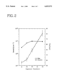
- FIG. 2 is a graph illustrating dependence of the average diameter and the density of Ga-droplets on the supplied amount of TEGa
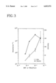
- FIG. 3 is a graph illustrating effect of a beam equivalent pressure (BEP) of TEGa on the density and average diameter of Ga-droplets;
- BEP beam equivalent pressure
- FIG. 4 is a graph showing dependence of the density and the average size of Ga-droplets as a function of growth temperature
- FIG. 5 is a graph showing effect of misorientation angle of GaAs substrate on the density and the average size of Ga-droplets
- FIG. 6 shows an SEM (Scanning Electron Microscopy) micrograph of Ga-droplets formed on GaAs substrate according to the present invention.
- FIG. 7 shows an AFM (Automic Force Microscope) image of GaAs islands grown by this invention.
- FIG. 1 there is shown a heterojunction structure manufactured in accordance with the present invention.
- Samples were grown in a modified CBE apparatus which consists of an ultrahigh vacuum growth chamber and a gas source control system. Cr-doped GaAs (100) substrate 11 were used. Prior to the growth, the GaAs substrate 11 was heated to remove adsorbed impurity and surface oxide layers. And then, a GaAs buffer layer 12 and a AlGaAs barrier 13 are sequentially grown on the GaAs substrate 11.
- the subsequent supply of Group Ill or V sources were performed at growth temperatures between 420 to 550° C.
- the growth sequence of Ga-droplets is as follows. After the temperature of the GaAs substrate 11 reached the growth temperature, TEGa (triethylgallium) was supplied onto the sample, where the Ga-droplets were formed. Then, arsine (AsH 3 ) was supplied again a few seconds later after stopping the TEGa supply. Then, the substrate temperature was decreased under arsine supply. As a result, GaAs quantum dots 14 are formed.
- Ga-droplets For successfully growing high-quality GaAs quantum dots by Ga-droplet-induced CBE using TEGa and thermally cracked arsine, the formation of Ga-droplets, whose characteristics depend not only on the growth parameters but also on the misorientation angle of substrates, is required to be optimized under various growth conditions.
- FIG. 2 shows the dependence of the average diameter and the density of Ga-droplets on the amount of TEGa supplied at the growth temperature of 470° C. under a beam equivalent pressure of 2 ⁇ 10 5 Torr.
- the density and size distribution was obtained by using high-resolution scanning electron microscope (HRSEM).
- HRSEM high-resolution scanning electron microscope
- the size and the density of Ga-droplets increased with the increase in the amount of TEGa supplied.
- the change of density of Ga-droplets was negligible after 20 seconds exposure of TEGa, but the size of Ga-droplets monotonically increased with the increase of exposure time of TEGa.
- the standard deviation of the size distribution of the Ga-droplet is about 10% in all samples observed.
- the major process is the growth of Ga-droplets with the increase in the amount of TEGa supplied. Since the distance between droplets is small compared to the diffusion length of Ga-adspecies, all the Ga-adspecies decomposed between the droplets are captured by the neighbor droplets after a certain amount of TEGa is supplied. Consequently, the size of Ga-droplets increase depending on the amount of TEGa supplied without variation of droplet density. As shown in FIG. 2, it can be seen that an optimal exposure time of TEGa is a range of about 20-30 seconds.
- FIG. 3 shows the effect of the BEP of TEGa on the density and average diameter of Ga-droplets formed on the surface during the Ga-droplet formation process.
- the samples were grown at a growth temperature of 470° C. with the same TEGa exposure time (30 sec.).
- the formation of Ga-droplets was not observed on the sample surface.
- the density of Ga-droplets increased by increasing the BEP of TEGa supplied and then decreased in the high BEP regions.
- the increase of Ga-droplet density can be understood by considering the classical nucleation theory at solid vapor interface.
- the density of Ga-droplets started to decrease beyond the BEP of 1.0 ⁇ 10 4 Torr.
- the optimized growth condition of BEP is in the range of 1 ⁇ 10 -4 ⁇ 5 ⁇ 10 -5 Torr as shown in FIG. 3.
- FIG. 4 shows the dependence of density and size of Ga-droplets as a function of growth temperature from 420 to 550° C. at the BEP of 2 ⁇ 10 -5 Torr.
- the growth temperature of 420° C. no indication of Ga-droplet formation on the grown surface was observed using HRSEM. This may be due to the limitation of TEGa decomposition at the low growth temperature.
- the supersaturated Ga-adspecies were not efficiently formed on the surface for the nucleation of Ga-droplets.
- the density of Ga-droplets decreased with increasing growth temperature of up to 550° C.
- the fact that the decrease of density of Ga-droplets depends on the growth temperature is consistent with the temperature dependence of classical nucleation theory.
- optimal temperature of the substrate is about 450 to 470° C.
- FIG. 5 shows the effect of misorientation angle of GaAs substrate on the density and the size of Ga-droplets at the growth temperature of 470° C.
- the creation of the Ga-droplets was performed on (100) GaAs substrates with 0°, 2°, 4°, and 8° off toward [110] at the BEP of TEGa of 2.0 ⁇ 10 -5 Torr. Growth on an exact and on a slightly misoriented surface (2° off toward [110]) showed similar features regarding both the density and size of created Ga-droplets.
- the density of droplets was nearly the same as that on an exactly oriented GaAs surface.
- the size of Ga-droplets increased with decreasing density of Ga-droplets on the highly misoriented substrates. This tendency is attributed to the fact that the size of Ga-droplet is inversely proportional to the density under the same amount of TEGa supplied.
- FIG. 6 shows a SEM micrograph of Ga-droplets formed by the supply of TEGa corresponding to about six monolayers at a substrate temperature of 470° C.
- the Ga droplets show a round shape with diameter of about 50 nanometers, height of about 20 nanometers, and density of 1 ⁇ 10 9 cm.sup. -2, and are formed without any process prior to the growth.
- FIG. 7 shows the AFM image of GaAs islands grown by Ga-droplet formation and successive supply of arsine.
- the GaAs islands are observed in round shape each with a diameter of about 50nm and a height of about 10nm, and were formed without any process prior to the growth. It is confirmed the formation of GaAs islands from Ga-droplets using cross-sectional transmission electron microscopy (TEM) with atomic resolution. Well-defined zinc-blend structure of GaAs islands were coherently grown on the GaAs buffer layer. It is quite different from the conventional MBE (Molecular Beam Epitaxy). In MBE growth, Ga-droplets disappear after As molecular beam supply is directed to GaAs surface.
- MBE Molecular Beam Epitaxy
- the droplet epitaxy technique of MBE is quite complicated and requires a number of steps to obtain an inert surface with appropriate dangling bonds suitable for supporting the adhesion of foreign atoms.
- GaAs islands can be grown on bare GaAs surface by Ga-droplet-induced CBE without any pretreatment step. This phenomenon can be attributed to the passivation effect of the Ga-droplet by hydrogen and hydrocarbon radicals dissociated from arsine and TEGa during the Ga-droplet-induced CBE.
- high-quality GaAs quantum dots are easy to grow from Ga-droplets which are successively supplied with arsine with neither pattern definition nor pre-treatment steps prior to the growth.
- the growth of high-density GaAs quantum dots can be achieved by a simple change of source supply mode and their characteristics were found to depend not only on the growth conditions but also on the substrate misorientations.
- Ga-droplet-induced chemical beam epitaxy can be a very effective method to grow quantum dots, even in lattice-matched material systems unlike Stranski-Krastanow growth.
Abstract
Description
Claims (10)
Applications Claiming Priority (2)
| Application Number | Priority Date | Filing Date | Title |
|---|---|---|---|
| KR97-62773 | 1997-11-15 | ||
| KR1019970062773A KR100249774B1 (en) | 1997-11-25 | 1997-11-25 | Growing method of high quality gaas quantum dots |
Publications (1)
| Publication Number | Publication Date |
|---|---|
| US6033972A true US6033972A (en) | 2000-03-07 |
Family
ID=19525563
Family Applications (1)
| Application Number | Title | Priority Date | Filing Date |
|---|---|---|---|
| US09/135,124 Expired - Lifetime US6033972A (en) | 1997-11-15 | 1998-08-17 | Growing method of GaAs quantum dots using chemical beam epitaxy |
Country Status (2)
| Country | Link |
|---|---|
| US (1) | US6033972A (en) |
| KR (1) | KR100249774B1 (en) |
Cited By (12)
| Publication number | Priority date | Publication date | Assignee | Title |
|---|---|---|---|---|
| WO2001071812A1 (en) * | 2000-03-23 | 2001-09-27 | Mp Technologies Llc | Quantum dots infrared for optoelectronic devices |
| US6329668B1 (en) | 2000-07-27 | 2001-12-11 | Mp Technologies L.L.C. | Quantum dots for optoelecronic devices |
| US6544808B2 (en) * | 2000-03-04 | 2003-04-08 | Nmctek Co., Ltd. | Light-emitting device with quantum dots and holes, and its fabricating method |
| WO2003098697A1 (en) | 2002-05-22 | 2003-11-27 | Fujitsu Limited | Method for forming quantum dot, quantum semiconductor device, and its manufacturing method |
| US6774560B1 (en) | 2000-09-19 | 2004-08-10 | The Regents Of The University Of California | Material system for tailorable white light emission and method for making thereof |
| US20040168626A1 (en) * | 2001-07-20 | 2004-09-02 | Peter Moeck | Process for forming semiconductor quantum dots with superior structural and phological stability |
| WO2005106984A1 (en) * | 2004-04-26 | 2005-11-10 | Epiplus Co., Ltd. | Method for fabricating semiconductor epitaxial layers using metal islands |
| US20060269745A1 (en) * | 2005-02-25 | 2006-11-30 | Samsung Electronics Co., Ltd. | Nano wires and method of manufacturing the same |
| US20070128839A1 (en) * | 2005-12-06 | 2007-06-07 | Jin Soo Kim | Quantum dot laser diode and method of manufacturing the same |
| US20100260223A1 (en) * | 2005-12-06 | 2010-10-14 | Jin Soo Kim | Quantum dot laser diode and method of fabricating the same |
| US20110084251A1 (en) * | 2008-06-17 | 2011-04-14 | National Research Council Of Canada | Atomistic quantum dot |
| JP2017188670A (en) * | 2014-05-26 | 2017-10-12 | 宇辰 張 | Zero dimensional electronic device and manufacturing method of the same |
Families Citing this family (3)
| Publication number | Priority date | Publication date | Assignee | Title |
|---|---|---|---|---|
| KR100319300B1 (en) * | 2000-03-23 | 2002-01-04 | 윤종용 | Semiconductor Device with Quantum dot buffer in heterojunction structures |
| KR100430813B1 (en) * | 2001-08-20 | 2004-05-10 | 재단법인서울대학교산학협력재단 | Two-step growth interruption process for control of semiconductor quantum dot |
| KR100599357B1 (en) * | 2005-01-12 | 2006-07-12 | 한국과학기술연구원 | Method for fabricating semiconductor device having quantum dot structure |
Citations (5)
| Publication number | Priority date | Publication date | Assignee | Title |
|---|---|---|---|---|
| US5229320A (en) * | 1991-08-02 | 1993-07-20 | Sony Corporation | Method for forming quantum dots |
| US5281543A (en) * | 1991-05-17 | 1994-01-25 | International Business Machines Corporation | Fabrication method for quantum devices in compound semiconductor layers |
| US5482890A (en) * | 1994-10-14 | 1996-01-09 | National Science Council | Method of fabricating quantum dot structures |
| US5543354A (en) * | 1993-11-25 | 1996-08-06 | Nippon Telegraph And Telephone Corporation | Method of fabricating a quantum dot structure on a (n11) substrate |
| US5614435A (en) * | 1994-10-27 | 1997-03-25 | The Regents Of The University Of California | Quantum dot fabrication process using strained epitaxial growth |
-
1997
- 1997-11-25 KR KR1019970062773A patent/KR100249774B1/en not_active IP Right Cessation
-
1998
- 1998-08-17 US US09/135,124 patent/US6033972A/en not_active Expired - Lifetime
Patent Citations (5)
| Publication number | Priority date | Publication date | Assignee | Title |
|---|---|---|---|---|
| US5281543A (en) * | 1991-05-17 | 1994-01-25 | International Business Machines Corporation | Fabrication method for quantum devices in compound semiconductor layers |
| US5229320A (en) * | 1991-08-02 | 1993-07-20 | Sony Corporation | Method for forming quantum dots |
| US5543354A (en) * | 1993-11-25 | 1996-08-06 | Nippon Telegraph And Telephone Corporation | Method of fabricating a quantum dot structure on a (n11) substrate |
| US5482890A (en) * | 1994-10-14 | 1996-01-09 | National Science Council | Method of fabricating quantum dot structures |
| US5614435A (en) * | 1994-10-27 | 1997-03-25 | The Regents Of The University Of California | Quantum dot fabrication process using strained epitaxial growth |
Non-Patent Citations (8)
| Title |
|---|
| D.S.L. Mui et al., "Surface Migration Induced self-aligned InAs islands grown by molecular beam epitaxy", pp. 1620-1622. Applied Physics Letters 66 (13) Mar. 95. |
| D.S.L. Mui et al., Surface Migration Induced self aligned InAs islands grown by molecular beam epitaxy , pp. 1620 1622. Applied Physics Letters 66 (13) Mar. 95. * |
| Lee et al., "Chemical beam epitaxial growth of InGaAs quantum dots using the droplet rechnique"; Ungyong Mulli, vol. 10, No. 3, p. 235-240, May 1997. |
| Lee et al., Chemical beam epitaxial growth of InGaAs quantum dots using the droplet rechnique ; Ungyong Mulli, vol. 10, No. 3, p. 235 240, May 1997. * |
| M. Kitamura et al., "In situ fabrication of self-aligned InGaAs quantum dots on GaAs multiatomic steps by metalorganic chemical vapor deposition", pp. 3663-3665. Applied Physic Letter 66 (26) Jun. 95. |
| M. Kitamura et al., In situ fabrication of self aligned InGaAs quantum dots on GaAs multiatomic steps by metalorganic chemical vapor deposition , pp. 3663 3665. Applied Physic Letter 66 (26) Jun. 95. * |
| Zh. I. Alferov et al., "An injection heterojunction laser based on arrays of vertically coupled InAs quantum dots in a GaAs matrix", pp. 194-196. Semiconductors 30(2) Feb. 96. |
| Zh. I. Alferov et al., An injection heterojunction laser based on arrays of vertically coupled InAs quantum dots in a GaAs matrix , pp. 194 196. Semiconductors 30(2) Feb. 96. * |
Cited By (28)
| Publication number | Priority date | Publication date | Assignee | Title |
|---|---|---|---|---|
| US6544808B2 (en) * | 2000-03-04 | 2003-04-08 | Nmctek Co., Ltd. | Light-emitting device with quantum dots and holes, and its fabricating method |
| US6753545B2 (en) | 2000-03-04 | 2004-06-22 | Nmctek Co. Ltd. | Light-emitting device with quantum dots and holes, and its fabricating method |
| WO2001071812A1 (en) * | 2000-03-23 | 2001-09-27 | Mp Technologies Llc | Quantum dots infrared for optoelectronic devices |
| US7718001B2 (en) | 2000-04-26 | 2010-05-18 | Galaxia Photonics Co., Ltd. | Method for fabricating semiconductor epitaxial layers using metal islands |
| US6329668B1 (en) | 2000-07-27 | 2001-12-11 | Mp Technologies L.L.C. | Quantum dots for optoelecronic devices |
| US6774560B1 (en) | 2000-09-19 | 2004-08-10 | The Regents Of The University Of California | Material system for tailorable white light emission and method for making thereof |
| US20040168626A1 (en) * | 2001-07-20 | 2004-09-02 | Peter Moeck | Process for forming semiconductor quantum dots with superior structural and phological stability |
| US20080067498A1 (en) * | 2002-05-22 | 2008-03-20 | Fujitsu Limited | Method for forming quantum dot, and quantum semiconductor device and method for fabricating the same |
| US7755080B2 (en) | 2002-05-22 | 2010-07-13 | Fujitsu Limited | Method for forming quantum dot, and quantum semiconductor device and method for fabricating the same |
| US7307030B2 (en) | 2002-05-22 | 2007-12-11 | Fujitsu Limited | Method for forming quantum dot, and quantum semiconductor device and method for fabricating the same |
| US20050173695A1 (en) * | 2002-05-22 | 2005-08-11 | Hai-Zhi Song | Method for forming quantum dot, and quantum semiconductor device and method for fabricating the same |
| WO2003098697A1 (en) | 2002-05-22 | 2003-11-27 | Fujitsu Limited | Method for forming quantum dot, quantum semiconductor device, and its manufacturing method |
| EP2096670A2 (en) | 2002-05-22 | 2009-09-02 | Fujitsu Ltd. | Quantum semiconductor device and method for fabricating the same |
| WO2005106984A1 (en) * | 2004-04-26 | 2005-11-10 | Epiplus Co., Ltd. | Method for fabricating semiconductor epitaxial layers using metal islands |
| US20090148976A1 (en) * | 2004-04-26 | 2009-06-11 | Sung-Hoon Jung | Method for fabricating semiconductor epitaxial layers using metal islands |
| US20060269745A1 (en) * | 2005-02-25 | 2006-11-30 | Samsung Electronics Co., Ltd. | Nano wires and method of manufacturing the same |
| US7575943B2 (en) | 2005-12-06 | 2009-08-18 | Electronics And Telecommunications Research Institute | Quantum dot laser diode and method of manufacturing the same |
| US20090296766A1 (en) * | 2005-12-06 | 2009-12-03 | Jin Soo Kim | Quantum dot laser diode and method of manufacturing the same |
| US20070128839A1 (en) * | 2005-12-06 | 2007-06-07 | Jin Soo Kim | Quantum dot laser diode and method of manufacturing the same |
| US20100260223A1 (en) * | 2005-12-06 | 2010-10-14 | Jin Soo Kim | Quantum dot laser diode and method of fabricating the same |
| US20110165716A1 (en) * | 2005-12-06 | 2011-07-07 | Electronics And Telecommunications Research Institute | Quantum dot laser diode and method of fabricating the same |
| US9006749B2 (en) | 2005-12-06 | 2015-04-14 | Electronics And Telecommunications Research Institute | Quantum dot laser diode and method of manufacturing the same |
| US20110084251A1 (en) * | 2008-06-17 | 2011-04-14 | National Research Council Of Canada | Atomistic quantum dot |
| US8816479B2 (en) | 2008-06-17 | 2014-08-26 | National Research Council Of Canada | Atomistic quantum dot |
| US9213945B2 (en) | 2008-06-17 | 2015-12-15 | National Research Council Of Canada | Method for controlling quantum dot device by perturbing dangling bond electronic states |
| US9400957B2 (en) | 2008-06-17 | 2016-07-26 | National Research Council Of Canada | Method for quantum computation by perturbing dangling bond electronic states |
| US9704101B2 (en) | 2008-06-17 | 2017-07-11 | National Research Council Of Canada | Method for operating an electronic state device by perturbating dangling bond electronic states |
| JP2017188670A (en) * | 2014-05-26 | 2017-10-12 | 宇辰 張 | Zero dimensional electronic device and manufacturing method of the same |
Also Published As
| Publication number | Publication date |
|---|---|
| KR100249774B1 (en) | 2000-03-15 |
| KR19990042070A (en) | 1999-06-15 |
Similar Documents
| Publication | Publication Date | Title |
|---|---|---|
| US6033972A (en) | Growing method of GaAs quantum dots using chemical beam epitaxy | |
| JP7009358B2 (en) | How to grow nanowires or nanopyramids on a graphite substrate | |
| US5614435A (en) | Quantum dot fabrication process using strained epitaxial growth | |
| JP5483887B2 (en) | Method for synthesis of epitaxial semiconductor nanowires on Si without metal | |
| KR100301116B1 (en) | Method for producing a compound semiconductor substrate having a quantum dot structure | |
| US20080318003A1 (en) | Nanostructures and Method of Making the Same | |
| KR20180053640A (en) | Nanowires or nano-pyramids grown on a graphite substrate | |
| Detz et al. | Lithography-free positioned GaAs nanowire growth with focused ion beam implantation of Ga | |
| US6696372B2 (en) | Method of fabricating a semiconductor structure having quantum wires and a semiconductor device including such structure | |
| US5346581A (en) | Method of making a compound semiconductor device | |
| Borgstrom et al. | Electron beam prepatterning for site control of self-assembled quantum dots | |
| JP3251236B2 (en) | Manufacturing method of semiconductor quantum dots | |
| Fukui et al. | Multiatomic step formation mechanism of metalorganic vapor phase epitaxial grown GaAs vicinal surfaces and its application to quantum well wires | |
| JP2007007827A (en) | Method for manufacturing nanostructure | |
| Ro et al. | Ga-droplet-induced formation of GaAs nano-islands by chemical beam epitaxy | |
| Ro et al. | Formation of GaAs island by Ga-droplet-induced chemical beam epitaxy | |
| JP4041887B2 (en) | Method for forming antimony quantum dots | |
| JP3402425B2 (en) | Manufacturing method of semiconductor fine structure | |
| WO2023037490A1 (en) | Nanowires and method for producing same | |
| Ishikawa et al. | Nanometer‐scale pattern formation of GaAs by in situ electron‐beam lithography using surface oxide layer as a resist film | |
| JP2004281954A (en) | Method of manufacturing quantum dot | |
| Ahopelto et al. | Fabrication of nanostructures using MBE and MOVPE | |
| Patrick Tung et al. | Periodic Two-Dimensional GaAs and InGaAs Quantum Rings Grown on GaAs (001) by Droplet Epitaxy | |
| Ro et al. | Size distribution of quantum-scale GaAs islands grown by Ga droplet induced chemical beam epitaxy | |
| Ro et al. | Fabrication of self-assembled InGaAs, GaAs, and InAs quantum dots by chemical beam epitaxy |
Legal Events
| Date | Code | Title | Description |
|---|---|---|---|
| AS | Assignment |
Owner name: ELECTRONICS AND TELECOMMUNICATIONS RESEARCH INSTIT Free format text: ASSIGNMENT OF ASSIGNORS INTEREST;ASSIGNORS:RO, JEONG RAE;KIM, SUNG BOCK;LEE, EL HANG;REEL/FRAME:009403/0874 Effective date: 19980807 |
|
| FEPP | Fee payment procedure |
Free format text: PAYOR NUMBER ASSIGNED (ORIGINAL EVENT CODE: ASPN); ENTITY STATUS OF PATENT OWNER: SMALL ENTITY |
|
| STCF | Information on status: patent grant |
Free format text: PATENTED CASE |
|
| FPAY | Fee payment |
Year of fee payment: 4 |
|
| FPAY | Fee payment |
Year of fee payment: 8 |
|
| FEPP | Fee payment procedure |
Free format text: PAYER NUMBER DE-ASSIGNED (ORIGINAL EVENT CODE: RMPN); ENTITY STATUS OF PATENT OWNER: SMALL ENTITY Free format text: PAYOR NUMBER ASSIGNED (ORIGINAL EVENT CODE: ASPN); ENTITY STATUS OF PATENT OWNER: SMALL ENTITY |
|
| FPAY | Fee payment |
Year of fee payment: 12 |