EP0883331B1 - Electroplating process - Google Patents
Electroplating process Download PDFInfo
- Publication number
- EP0883331B1 EP0883331B1 EP98109457A EP98109457A EP0883331B1 EP 0883331 B1 EP0883331 B1 EP 0883331B1 EP 98109457 A EP98109457 A EP 98109457A EP 98109457 A EP98109457 A EP 98109457A EP 0883331 B1 EP0883331 B1 EP 0883331B1
- Authority
- EP
- European Patent Office
- Prior art keywords
- substrate
- solution
- dispersion
- copper
- graphite
- Prior art date
- Legal status (The legal status is an assumption and is not a legal conclusion. Google has not performed a legal analysis and makes no representation as to the accuracy of the status listed.)
- Expired - Lifetime
Links
Images


Classifications
-
- H—ELECTRICITY
- H05—ELECTRIC TECHNIQUES NOT OTHERWISE PROVIDED FOR
- H05K—PRINTED CIRCUITS; CASINGS OR CONSTRUCTIONAL DETAILS OF ELECTRIC APPARATUS; MANUFACTURE OF ASSEMBLAGES OF ELECTRICAL COMPONENTS
- H05K3/00—Apparatus or processes for manufacturing printed circuits
- H05K3/40—Forming printed elements for providing electric connections to or between printed circuits
- H05K3/42—Plated through-holes or plated via connections
- H05K3/423—Plated through-holes or plated via connections characterised by electroplating method
- H05K3/424—Plated through-holes or plated via connections characterised by electroplating method by direct electroplating
-
- C—CHEMISTRY; METALLURGY
- C25—ELECTROLYTIC OR ELECTROPHORETIC PROCESSES; APPARATUS THEREFOR
- C25D—PROCESSES FOR THE ELECTROLYTIC OR ELECTROPHORETIC PRODUCTION OF COATINGS; ELECTROFORMING; APPARATUS THEREFOR
- C25D5/00—Electroplating characterised by the process; Pretreatment or after-treatment of workpieces
- C25D5/54—Electroplating of non-metallic surfaces
- C25D5/56—Electroplating of non-metallic surfaces of plastics
Definitions
- This invention relates to a process for fabrication of printed circuit boards. More particularly, this invention relates to a metallization process for printed circuit board manufacture using a carbonaceous coating as a conductive layer for direct electroplating. More specifically, this invention has for its object a direct plate process involving fewer processing steps which process provides a printed circuit board exhibiting a significantly reduced incidence of interconnect defects.
- Nonconducting surfaces are conventionally metallized by a sequence of steps comprising catalysis of the surface of the nonconductor to render the same catalytic to electroless metal deposition followed by contact of the catalyzed surface with an electroless plating solution that deposits metal over the catalyzed surface in the absence of an external source of electricity. Metal plating continues for a time sufficient to form a metal deposit of the desired thickness. Following electroless metal deposition, the electroless metal deposit is optionally enhanced by electrodeposition of metal over the electroless metal coating to a desired thickness. Electrolytic deposition is possible because the electroless metal deposit serves as a conductive coating that permits electroplating.
- Catalyst compositions useful for electroless metal plating are known in the art and disclosed in numerous publications including U.S. Pat. No. 3,011,920.
- the catalyst of this patent consists of an aqueous suspension of a tin/noble catalytic metal colloid. A surface treated with such a catalyst promotes the generation of an electrolessly formed metal deposit by the oxidation of a reducing agent in an electroless plating solution catalyzed by the catalytic colloid.
- Electroless plating solutions are aqueous solutions containing both a dissolved metal and a reducing agent in solution.
- the presence of the dissolved metal and reducing agent together in solution results in plate out of the metal in contact with a catalytic metal tin catalyst.
- the presence of the dissolved metal and reducing agent together in solution may also result in solution instability and indiscriminate deposition of metal on the walls of containers for such plating solutions. This may necessitate interruption of the plating operation, removal of the plating solution from the tank and cleaning of tank walls and bottoms by means of an etching operation. Indiscriminate deposition may be avoided by careful control of the plating solution during use and by use of stabilizers in solution which inhibit indiscriminate deposition, but also retard plating rate.
- deposition begins at the interface of a conductive surface and the catalyzed nonconductive surface.
- the deposit grows epitaxially along the catalyzed surface from this interface. For this reason, metal deposition onto the substrate using this process is slow.
- deposit thickness is uneven with the thickest deposit occurring at the interface with the conductive surface and the thinnest deposit occurring at a point most remote from the interface.
- the additive in the electroplating solution responsible for inhibiting deposition is described as one selected from a group of dyes, surfactants, chelating agents, brighteners and leveling agents. Many of such materials are conventional additives for electroplating solutions.
- the coating formed is both more robust and more conductive and electroless plating catalyst does not desorb from the surface during metallization. Consequently, in accordance with the process of said patents, it is possible to form printed circuit boards using formulations that would otherwise attack the catalyst layer such as those solutions used in pattern plating processes.
- the coating formed from the carbon black dispersion is only poorly adherent to the underlying substrate and has a tendency to flake off of the substrate prior to the plating step. This results in void formation during plating.
- the metal deposit is a tendency for the metal deposit to separate from the substrate. This can lead to interconnect defects between a metallized hole and an innerlayer in multilayer printed circuit fabrication.
- carbon black is suspected to be carcinogenic to humans.
- a process for electroplating the walls of through holes in a laminated printed wiring board is disclosed in U.S. Patent No. 5,015,339.
- the process disclosed in this patent involves the treatment of the walls of through holes with a single neutralizer/conditioner solution which comprises a mixture of water, at least one neutral or acidic reducing agent, and at least one polyelectrolyte polymer conditioner. Afterwards the walls of the through holes are coated with a dispersion of carbon black followed by electroplating a metal layer over the carbon black layer.
- a more recently utilized direct plate process for metallizing the walls of hole-walls employs dispersions of graphite for the formation of a conductive coating.
- the use of graphite to form conductive coatings on through-hole walls is known and disclosed in U.S. Patent No. 2,897,409.
- Current processes are disclosed, for example, in U.S. Patents No. 4,619,741; 5,389,270 and 5,611,905.
- a dispersion of carbon black or graphite is passed through the through-holes to form a coating of the dispersion on the through hole-walls.
- the coating is dried to yield a conductive layer of the carbon black or graphite which is sufficiently conductive for electroplating in a conventional manner.
- a typical process for the manufacture of a multilayer printed circuit board using graphite coatings, excluding water rinses includes the steps of solvent pretreatment to soften the epoxy circuit board substrate, treatment with an oxidizing agent such as a permanganate solution to form a porous structure and to activate the surface of the epoxy substrate, treatment with a neutralizer to remove permanganate residue, an optional treatment step with a glass etchant, treatment with a solution of a charge modifier to cause adsorption of a subsequently applied graphite layer, formation of the graphite layer by immersion of the substrate in an aqueous graphite dispersion, several drying steps to bond the graphite coating to the epoxy surface, treatment with a microetchant to remove graphite from copper surfaces without removing the same from epoxy surfaces, pattern formation and plating.
- solvent pretreatment to soften the epoxy circuit board substrate
- an oxidizing agent such as a permanganate solution to form a porous structure and to activate the surface of the epoxy substrate
- treatment with a neutralizer to
- the overall process is unduly long in the number of processing steps. In addition, it has been found that the process results in a significant number of interconnect defects (ICDs) and voids in the finished circuit resulting in disposal or reworking of the boards containing these defects.
- ICDs interconnect defects
- the present invention is directed to an improved process for the direct electroplating of a printed circuit board substrate using a dispersion of carbon black or graphite particles, hereinafter referred to collectively as a carbonaceous coating or a carbonaceous dispersion as the context so requires.
- a single treatment solution is used to replace prior art solutions used to neutralize and remove permanganate residue and charge modify the surface of a circuit board substrate.
- the single solution contains a hydroxyl substituted lower molecular weight amine, a polyelectrolyte and an organic acid.
- the subject invention provides the advantage of combining several treatment solutions into a single solution thereby reducing the number of processing steps, for reasons not fully understood, the invention also significantly reduces the incidence of interconnect defects and voids in circuit manufacture.
- the subject invention is suitable for the manufacture of a variety of commercial articles where a metal deposit is desired over the surface of a nonconductor.
- the invention is especially useful for fabrication of printed circuit boards having copper cladding over at least one surface of a printed circuit board substrate. For this reason, the description that follows is directed primarily to printed circuit board manufacture.
- the substrate commonly used is an epoxy substrate filled with glass fibers and copper clad on at least one of its surfaces, or for multilayer circuit manufacture, an innerlayer clad with copper.
- the epoxy can be mixed with other resins and glass fibers for specific purposes.
- Other circuit board substrates include polyimide, Teflon and flex films such as films of Mylar.
- a first step comprises the formation of through-holes by drilling or punching or any other method known to the art. These holes are subsequently metallized to provide conductive pathways between circuit layers.
- one step comprises formation of vias that are subsequently metallized to provide conductive pathways between circuit layers comprising the multilayer stack.
- Suitable organic solutions are oxygenated epoxy solvents such as those disclosed in U.S. Patent No. 4,515,829. Such solvents include acetone, methylethyl ketone, Methyl Cellosolve, Butyl Carbitol, Butyl Carbitol acetate and Butyl Cellosolve.
- hole walls are desmeared.
- Typical hole wall desmear involves treatment of the walls with sulfuric acid, chromic acid, permanganate, or plasma etching though the commonly used method involves treatment with permanganate.
- Permanganate solutions used are alkaline having a pH in excess of 11, typically a pH ranging from between 11.5 to 14.0. Permanganate is used in an amount of at least 2 grams per liter of solution.
- the circuit board base material may be treated with a glass etchant that removes glass fibers extending into the holes from the hole walls.
- a glass etchant that removes glass fibers extending into the holes from the hole walls.
- permanganate residues are removed with a solution that neutralizes base residues and dissolves manganate residues.
- solutions typically comprise an acidic peroxide or alkaline amine and a surfactant.
- the hole walls are charge modified to impart a charge to the hole wall opposite to the charge carried by the particles comprising the carbonaceous coating dispersion.
- the material of choice for the step of charge modification is a polyelectrolyte.
- Polyelectrolytes are typically polymers having a plurality of charged groups along their chains where the charged groups carry a charge opposite from the charge of a dispersed particle to be adsorbed onto the substrate.
- Polyelectrolytes used in metal plating procedures are disclosed in numerous publications including U.K. Patent No. 1,338,491 and U.S. Patents Nos. 4,478,883; 4,554,182; 4,701,350 and 4.969.979.
- Suitable reducing agents are disclosed in U.K. Patent Application 2,134,140A and in the above referenced U.S. Patent No. 4,515,829.
- Suitable reducing agents include stannous ions as provided in acidified stannous chloride solutions, bisulfite ions, hydroxylamines such as hydroxylamine chloride and hydroxylamine nitrate, formaldehyde, sugar, etc.
- the preferred reducing agent is a hydroxylamine such as hydroxyl amine nitrate used in a concentration of from about 1 to 100 grams per liter of solution and preferably, within a range of from 5 to 50 grams per liter.
- the single treatment solution also includes a polyelectrolyte.
- a polyelectrolyte is a macromolecular compound which, when dissolved in a suitable polar solvent, generally water, spontaneously acquires or can be made to acquire a large number of elementary charges distributed along its macromolecular chain.
- the use of polyelectrolytes in plating process is disclosed in the above referenced patents and in particular, U.S. Patents No. 4,478,883 and 4,701,350.
- the polyelectrolyte used in the composition of the invention is water soluble, and preferably contains a cationic group such as a quaternary phosphonium or quaternary ammonium group. Such materials are commercially known.
- the Reten polymers from Hercules Incorporated are suitable materials.
- the concentration of the polyelectrolyte may vary within broad limits and preferably varies between about 1 and 150 grams per liter and more preferably, between about 5 and 40 grams per liter.
- Preferred polyelectrolytes are polyquaternary amines.
- the third component of the formulation comprises an acid.
- weaker mineral acids may be used such as sulfuric acid and phosphoric acid, preferably the acid is an organic acid, more preferably a sulfonic acid and most preferably, a lower molecular weight alkyl sulfonic acid such as methane sulfonic acid, ethane sulfonic acid, etc.
- the sulfonic acid is used in an amount of from 20 to 150 grams per liter and more preferably, in an amount of from 50 to 100 grams per liter. In general, the amount of the acid is sufficient to provide a composition having a pH between 0 and 2.5 and preferably, between about 0.2 and 2.5.
- Suitable surfactants include Triton X-100 or Triton X-102, sold by Rohm and Haas Co., Philadelphia, Pennsylvania; Fluorad® FC-120, FC-430, FC-431, FC-129, and FC-135 anionic fluorochemical surfactants; sold by Minnesota Mining & Manufacturing Co.. St. Paul, Minnesota; Darvan No. 1, sold by R.T. Vanderbilt Co.; Eccowet LF, sold by Eastern Color and Chemical; Petro ULF, sold by Petro Chemical Co. Inc.; Polytergent B-Series surfactants, sold by Olin Corporation. Additional surfactants are disclosed in the above cited patents.
- the surfactant may be used in a concentration of from 1 to 50 grams per liter and more preferably, within a concentration of from 2 to 25 grams per liter.
- An optional additive in the formulation of the invention is a glass etchant to remove glass fibers protruding into the interior of the through-holes following desmear.
- a glass etchant to remove glass fibers protruding into the interior of the through-holes following desmear. Any known glass etchant may be used.
- a preferred glass etchant is ammonium bifluoride in an amount of from 1 to 25 grams per liter of solution.
- the single solution described above may be used in either vertical or horizontal processing procedures. It is preferably used at elevated temperatures and temperatures within the range of from 25 to 80°C are suitable, temperatures of from 40 to 50°C being more preferred.
- the solution may be applied to a substrate by immersion or spraying or any other means known to the art. If by immersion, the substrate to be treated is immersed in the solution for a time varying between 1 and 10 minutes and preferably for a time varying between 3 and 8 minutes. If by spraying, the time can be shortened to from 1/2 to 1 minute. Preferably, spraying is accomplished using submerged spray bars to prevent foaming.
- an interconnect defect is a separation failure between copper foil and plated copper within a hole wall due to inadequate bond between the copper foil cross section within the hole and plated copper. The failure may be due to residue left on the surface of the copper foil during processing.
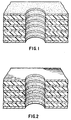
- FIG. 1 of the drawings a representation of a cross section of a multilayer board 1 is shown having via or through hole 2.
- the stack comprises a top copper clad layer 3, interconnect copper foils 4 separated by dielectric such as epoxy layers 5, and coated by carbonaceous coating 6.
- the carbonaceous coating is on the surface of copper cladding 3 and on the interface of copper foils 4 and dielectric surfaces 5 within the hole wall.
- Figure 2 of the drawings illustrates a hole wall where the carbonaceous coating is properly removed.
- Figure 4 of the drawing is a photomicrograph of the cross section of a through hole and shows proper bond between copper foil and plated copper.
- Figure 5 is a photomicrograph showing an interconnect defect such as might result from inadequate removal of the graphite as illustrated in Figure 3.
- the incidence of ICDs may be as high as 30 percent.
- the incidence of ICDs drops to 2 percent or less and typically less than 1 percent, all other process steps remaining the same.
- the next step in the process comprises treating the substrate with a carbonaceous dispersion.
- the particles may be of carbon black (amorphous), graphite (crystalline), or a mixture of the two.
- the carbonaceous material may be present in the dispersion in an amount of from about 0.1 to about 20% by weight of the dispersion, and preferably in an amount of from about 0.5 to about 10% by weight of the dispersion.
- the carbon may have a mean particle size within a range of from about 0.05 to about 50 microns, and preferably, is of a particle size within a range of from about 0.1 to 5.0 microns. From the perspective of performance, particles having the smaller dimension are preferred.
- Graphite particles of suitable size can be prepared by the wet grinding or milling of raw graphite having a particle size greater than 50 microns to form a slurry of smaller particles.
- Graphite particles of suitable size can also be formed by graphitizing already-small carbon-containing particles.
- the carbon black may have a substantially smaller particle size than the graphite.
- the ratio of graphite to carbon black may vary from about 1:100 to about 100:1, and preferably from about 1:10 to about 10:1.
- the carbon black used to form a carbonaceous dispersion may be substantially as described in U.S. Patent No. 5,139,642.
- Several commercial carbon blacks contemplated to be useful herein include Cabot Monarch 1300, sold by Cabot Corporation, Boston, Massachusetts; Cabot XC-72R Conductive, from the same manufacturer; Acheson Electrodag 230, sold by Acheson Colloids Co., Port Huron, Michigan; Columbian Raven 3500, made by Columbian Carbon Co., New York City. New York; and other conductive carbon blacks having similar particle sizes and dispersion characteristics.
- the graphite may be substantially as described in U.S. patent No. 5,139,642 and may be either synthetic or naturally occurring. Suitable commercial graphite and graphite dispersions contemplated to be useful herein include: Ultrafine Graphite sold by Showa Denko K.K., Tokyo, Japan; Aquadag E sold by Acheson Colloids of Port Huron, Michigan; Micro 440 and Graphite 850, both sold by Asbury Graphite Mills Inc., of Asbury, New Jersey; Grafo 1204B, sold by Metal Lubricants Company, Harvey, Illinois; Graphokote 90, sold by Dixon Products, Lakehurst, New Jersey; Nippon AUP (0.7 micron), sold by Nippon Graphite Industries, Ltd., Ishiyama, Japan; Hitasol Ga-66M and 66-S sold by Hitachi Powdered Metals Co., Ltd of Matsudo City. Japan; and others having similar electrical and dispersion characteristics. Synthetic graphite is preferred. Synthetic graphite is formed by heat
- Another component that may be present in the carbonaceous dispersion is a water soluble or dispersible binding agent to bond the carbon particles to the substrate and to form a coherent coating.
- the binding agent is believed to assist adhesion of the dispersed carbon particles to the surface of the non-conductive (i.e., dielectric) substrate which is to be made conductive for electroplating.
- the binding agent may be present as from about 0% to about 15% by weight, and preferably from about 0.2 to about 10% by weight.
- the binding agent is preferably a natural or synthetic polymer, polymerizable monomer, or other viscous or solid material (or precursor thereof) that is capable of both adhering to the carbon particles and of receiving an anionic dispersing agent (as described below).
- the binding agent may be a water soluble or water dispersible material selected from the group consisting of mono- and polysaccharides (or, more broadly, carbohydrates and anionic polymers).
- Monosaccharide binding agents include tetroses, pentoses, and hexoses.
- Polysaccharide (including disaccharide and higher saccharides) binding agents include sucrose, maltose, fructose, lactose, stachyose, maltopentose, dextrin, cellulose, corn starch and polysaccharide gums.
- Polysaccharide gums include agar, arabic, xanthan, pectin, alginate, tragacanath, dextran and other gums.
- Derivative polysaccharides include cellulose acetates, cellulose nitrates, methylcellulose, and carboxymethylcellulose.
- Hemicellulose polysaccharides include d-gluco-d-mannans, d-galacto-d-gluco-d-mannans, and others.
- Anionic polymers include the alkylcelluloses or carboxyalkylcelluloses, their low- and medium-viscosity alkali metal salts (e.g. sodium carboxymethylcellulose, or "CMC”), cellulose ethers, and nitrocellulose.
- CMC carboxymethylcellulose
- the acrylics may also be used as binding agents.
- Typical acrylics include polymerizable monomers and polymers, for example, emulsion polymers commonly known as acrylic latices.
- the monomers include acrylamide, acrylonitrile acrylic acid, methacrylic acid, glycidyl methacrylate and others.
- the acrylic polymers include polymers of any one or more of the foregoing monomers; polyacrylamide polymers; polyacrylic acid; acrylic ester polymers such as polymethyl acrylate, poly-ethyl acrylate, polypropyl acrylate, polyisopropyl acrylate, polybutyl acrylate, polyisobutyl acrylate, polypentyl acrylate, polyhexyl acrylate, polyheptyl acrylate, polyoctyl acrylate, and polyisobornyl acrylate; and other polyacrylates.
- binding agents may also be used such as vinyl resins including polyvinyl acetates, polyvinyl ethers, polyvinyl chlorides; pyrrolidone resins such as poly(N-vinyl-2-pyrrolidone); polyols such as polyvinyl alcohols and other materials that may be used as binding agents including polyethylenimine, methylaminoethyl resins, alkyltrimethylammonium chlorides, and others.
- a practical upper limit to the amount of binding agent used is that amount which materially interferes with the conductivity of the resulting conductive coatings by diluting the conductive solids in the composition after it is deposited as a film.
- a dispersing agent has a hydrophobic end and a hydrophilic end. It functions by surrounding the bound carbon particles thereby causing the particles to disperse. It is believed that the hydrophobic end of the dispersing agent is attracted to the hydrophobic region of the binding agent thereby causing the hydrophilic end to stick out into the aqueous surrounding dispersing medium.
- the sphere of charges surrounding each particle causes the particles to repel one another thus maintaining the dispersion stable.
- the amount of dispersing agent is an amount sufficient to cause the bound carbon particles to disperse in the aqueous dispersing medium.
- the amount used is dependent upon the size of the carbon particle and the amount of binding agent bound thereto.
- This amount of dispersing agent is the minimum effective amount of dispersing agent.
- Increasing amounts of dispersing agent may be added without adversely affecting the dispersion of the carbon particles.
- the dispersing agent may be anionic or cationic dependent on the charge of the dispersed phase.
- the dispersing agent may be present as from about 0% to about 10% by weight, and preferably about 0.01% to about 5% by weight.
- a practical upper limit to the amount of dispersing agents used is that amount which materially interferes with the conductivity of the resulting conductive coatings by diluting the conductive solids in the composition.
- Suitable anionic dispersing agents include acrylic latices, aqueous solutions of alkali metal polyacrylates, and similar materials.
- An optional component of the composition of the present invention is a surfactant.
- One function of the surfactant is to decrease the surface tension of the aqueous dispersing medium such that the aqueous dispersing medium containing the dispersed carbon particles is able to freely penetrate into the through holes or vias.
- a second function of the surfactant is to wet the surfaces of the polymeric and glass substrates. This facilitates the coating of these surfaces with the carbon dispersion.
- the amount of surfactant that is used will vary dependent upon the surfactant itself. When used, the amount of the surfactant may vary from about 0.01 % to about 10% by weight, and preferably in an amount of from about 0.02% to about 3% by weight of the composition.
- aqueous dispersing medium includes any solvent that is from 80 to 100% water wherein the balance of the material is a water soluble organic composition.
- Typical water soluble organic compositions include the low molecular weight alcohols, such as methanol, ethanol, and isopropanol.
- Additional organic components include solvents such as dimethylsulfoxide, tetrahydrofuran and ethylene or propylene glycol.
- the aqueous dispersing medium is 100% water.
- the composition and method of the present invention is capable of being run over a wide pH range such as from about 3.0 to 13.0, but preferably the composition has a pH of from about 8 to 13.0 and more preferably, a pH within the range of 9.0 to 11. Viscosity changes are encountered when the pH of the dispersion is within the acid range.
- the pH may be maintained by a pH buffer.
- the buffer functions by precluding or minimizing changes in pH such as may occur during the course of a run where a large number of boards are treated with the carbonaceous composition. The maintenance of a constant or nearly constant pH ensures reproducible results from board to board.
- a copper etchant or complexing agent compatible at the pH of the carbonaceous dispersion is also desirably added to the dispersion so that in use, the copper cladding may be etched simultaneously with the formation of the graphite coating.
- Copper etchants and complexing agents suitable for use within the useful pH range are known in the art and disclosed in numerous publications.
- a preferred class of materials are those materials used as complexing agents in electroless copper plating solutions. Such materials are disclosed in numerous prior publications including U.S. Patents Nos. 3,728,137 and 3,790,392.
- Such materials include, by way of example, Rochelle salts, the sodium salts of ethylenediamine tetraacetic acid, nitrolotriacetic acid and its alkali metal salts, triethanolamine, modified ethylenediamine tetraacetic acids such as N-hydroxyethylene diamine triacetate, hydroxyalkyl substituted dialkaline triamines such as pentahydroxypropyldiethylenetriamine and the like.
- One preferred class of amines are the hydroxyalkyl substituted tertiary amines such as tetrahydroxypropylethylene diamine, pentahydroxypropyl diethylene triamine, trihydroxypropyl amine, trihydroxypropyl hydroxyethylethylene diamine and the like.
- etchants are those materials used as relatively mild copper etchants, especially the amine based etchants.
- Such etchants are known in the art and disclosed in numerous publications including U.S. Patents Nos. 3.837,945 and 4,280,887.
- Such materials include, by way of example, ammonia and ammonium salts such as tetraamine cupric and cuprous salts and ammoniacal peroxy compounds as disclosed in the aforesaid patents.
- Quaternary ammonium hydroxides such as tetramethyl and tetraethyl ammonium hydroxide are also useful as etchants.
- the material used to add to the carbonaceous dispersion is one that is capable of complexing with the copper cladding to theoretically remove only the top monolayer of the copper cladding.
- the dissolution agent is one that should be of a strength sufficient to etch from about 0.01 to 50 microinches of copper and preferably, from 0.1 to 1.0 microinches of copper during that period of time that the carbonaceous coating material is in contact with the copper.
- the depth of penetration of the dissolution agent is controlled by pH, concentration, temperature and the amount of dissolved copper in the formulation.
- the etchant is added to the dispersion in an amount sufficient to etch copper as described above.
- the etchant is used in an amount of from about 0.1 to 10 percent by weight of the dispersion and more preferably, in an amount of from 0.5 to 5 percent by weight of the dispersion.
- the etchant is ammonium hydroxide as ammonium hydroxide provides adequate removal of copper ions from the surface of the cladding and may be used for close pH control.
- the carbonaceous dispersion is used in conventional manner. Using a copper clad substrate having apertures therein for purposes of illustration, the board would be cleaned, rinsed, treated with a neutralizer conditioner in accordance with the invention, and then treated with the dispersion. The dispersion would be applied to the substrate to form a wet coating. Thereafter, the coating would be dried to remove the dispersant, and in some processes but not all, fixed though this step does not appear to be critical. The carbonaceous coating would then be removed from metallic copper surfaces facilitated by the step of simultaneously etching the copper with the dispersion during the formation of the carbonaceous coating. For this reason, the carbonaceous coating may be removed without an additional etching or other chemical treatment step if desired. For example, pressure spraying may be used to remove the carbonaceous coating without a step of etching the copper though an optional etching step may be used in the process if desired.
- the part to be plated is used as a cathode in a conventional electroplating cell.
- Current density is conventional and varies typically within a range of from 10 through 80 amps/ft. 2 . In practice, it is convenient to initiate current flow as the part enters the plating solution. A preferred current density range is from 15 to 30 amps/ft. 2 .
- the plating solution is maintained at a temperature ranging between room temperature and about 40°C. Plating is continued for a time sufficient to form a deposit of desired thickness. For circuit board manufacture, a desired thickness may range between 0.5 and 2.0 mils, typically from 1 to 1.5 mils.
- a plating time of from 15 to 120 minutes is typically required to obtain a deposit of the preferred thickness within the preferred range of current densities.
- the deposit formed by the process is uniform in thickness, free of defects and strongly bonded to the surface of the nonconductor over which it is plated. Bond strength is satisfactory to withstand solder shock testing as conventionally used in printed circuit board manufacture.
- a dispersion is prepared by providing a preformed graphite dispersion obtained from Acheson Chemical Company and identified as Aquadag E. This dispersion contains about 3.0 percent by weight particulate graphite having a mean particle size of about 1 micron.
- the pH of the dispersion is adjusted to 10.5 by addition of ammonium hydroxide which functions as an etchant for copper and as a pH adjustor.
- a multilayer circuit board having 4 internal and 2 external circuit layers with an array of 14 and 36 mil. holes may be subjected to the following procedure.
- Step 1 Pre-clean and condition:
- Step 2 Form conductive particle coating:
- Step 3 Microetch copper surfaces and remove dispersion coating from copper cladding.
- the number of interconnect defects was less than 1 percent.
- the reducing solution is identified as Neutralizer 3314 and has the following composition: p-toluene sulfonic acid 10 grams per liter sulfuric acid (50% solution) 165 grams per liter hydrochloric acid (37% solution) 1 gram per liter surfactant 5 grams per liter hydrogen peroxide (35% solution) 50 grams per liter water to 1 liter
- the charge modification solution is identified as Sensitizer 2010 and has the following composition: potassium carbonate, anhydrous 7.00 grams per liter hydrochloric acid (37% solution) 0.01 grams per liter surfactant 1.50 grams per liter polyelectrolyte 6.00 grams per liter
- the number of interconnect defects was determined and found to be about 30.5 percent.
Landscapes
- Engineering & Computer Science (AREA)
- Chemical & Material Sciences (AREA)
- Chemical Kinetics & Catalysis (AREA)
- Electrochemistry (AREA)
- Materials Engineering (AREA)
- Metallurgy (AREA)
- Organic Chemistry (AREA)
- Manufacturing & Machinery (AREA)
- Microelectronics & Electronic Packaging (AREA)
- Electroplating Methods And Accessories (AREA)
- Manufacturing Of Printed Wiring (AREA)
- Chemically Coating (AREA)
Description
| hydroxyl ammonium nitrate (18% solution) | 54 grams per liter |
| methane sulfonic acid (70% solution) | 137 grams per liter |
| surfactant | 5 grams per liter |
| polyelectrolyte | 10 grams per liter |
| water | to 1 liter |
| p-toluene sulfonic acid | 10 grams per liter |
| sulfuric acid (50% solution) | 165 grams per liter |
| hydrochloric acid (37% solution) | 1 gram per liter |
| surfactant | 5 grams per liter |
| hydrogen peroxide (35% solution) | 50 grams per liter |
| water | to 1 liter |
| potassium carbonate, anhydrous | 7.00 grams per liter |
| hydrochloric acid (37% solution) | 0.01 grams per liter |
| surfactant | 1.50 grams per liter |
| polyelectrolyte | 6.00 grams per liter |
Claims (18)
- A process for depositing metal on a substrate having metallic and non-metallic regions and at least one hole passing therethrough, said process comprising the steps of treating the substrate with a single aqueous acid solution containing a reducing agent and a polyelectrolyte, contacting the so treated surface with an aqueous dispersion of carbonaceous particles to form a coating of said dispersion over all surfaces of said substrate and electroplating metal on said substrate from an electrolytic metal plating solution, characterized in that the aqueous acid solution has a pH varying between 0 and 2.5.
- The process of claim 1 characterized in that the pH varies between 0.5 and 1.5.
- The process of claim 1 or claim 2 characterized in that the reducing agent is a hydroxyl ammonium compound.
- The process of claim 3 characterized in that the hydroxyl ammonium compound is hydroxyl ammonium nitrate.
- The process of any one of claims 1 to 4 characterized in that the polyelectrolyte is a polyquaternary amine.
- The process of any one of claims 1 to 5 characterized in that the solution further contains a sulfonic acid.
- The process of any one of claims 1 to 6 characterized in that the solution contains a surfactant.
- The process of any one of claims 1 to 7 characterized in that the carbonaceous particles are selected from the group consisting of carbon black and graphite.
- The process of claim 8 characterized in that the carbonaceous particles are carbon black.
- The process of claim 8 characterized in that the carbonaceous particles are in the form of graphite.
- The process of any one of claims 1 to 10 characterized in that the metallic regions of the substrate are copper.
- A process for metallizing the walls of holes within a printed circuit board substrate having metallic and non-metallic regions, said process comprising the steps of treating the printed circuit board substrate with a single aqueous acid solution containing a hydroxyl ammonium reducing agent and a amine polyelectrolyte, contacting the so treated surface with an aqueous dispersion of carbonaceous particles to form a coating of said dispersion over all surfaces of said substrate and electroplating metal on said substrate from an electrolytic metal plating solution, characterized in that the aqueous acid solution has a pH varying between 0 and 2.5.
- The process of claim 12 characterized in that the pH varies between 0.5 and 1.5.
- The process of claim 12 or claim 13 characterized in that the hydroxyl ammonium compound is hydroxyl ammonium nitrate.
- The process of any one of claims 12 to 14 characterized in that the polyelectrolyte is a polyquaternary amine.
- The process of any one of claims 12 to 15 characterized in that the solution contains a sulfonic acid.
- The process of any one of claims 12 to 16 characterized in that the solution contains a surfactant.
- The process of any one of claims 12 to 17 characterized in that the carbonaceous particles are in the form of graphite.
Applications Claiming Priority (2)
| Application Number | Priority Date | Filing Date | Title |
|---|---|---|---|
| US868092 | 1997-06-03 | ||
| US08/868,092 US6565731B1 (en) | 1997-06-03 | 1997-06-03 | Electroplating process |
Publications (3)
| Publication Number | Publication Date |
|---|---|
| EP0883331A2 EP0883331A2 (en) | 1998-12-09 |
| EP0883331A3 EP0883331A3 (en) | 2001-08-01 |
| EP0883331B1 true EP0883331B1 (en) | 2005-12-21 |
Family
ID=25351058
Family Applications (1)
| Application Number | Title | Priority Date | Filing Date |
|---|---|---|---|
| EP98109457A Expired - Lifetime EP0883331B1 (en) | 1997-06-03 | 1998-05-25 | Electroplating process |
Country Status (5)
| Country | Link |
|---|---|
| US (1) | US6565731B1 (en) |
| EP (1) | EP0883331B1 (en) |
| JP (1) | JP4249291B2 (en) |
| KR (1) | KR100674116B1 (en) |
| DE (1) | DE69832845T2 (en) |
Families Citing this family (13)
| Publication number | Priority date | Publication date | Assignee | Title |
|---|---|---|---|---|
| TWI223678B (en) * | 1998-03-20 | 2004-11-11 | Semitool Inc | Process for applying a metal structure to a workpiece, the treated workpiece and a solution for electroplating copper |
| JP4055319B2 (en) * | 2000-02-18 | 2008-03-05 | ソニー株式会社 | Manufacturing method of semiconductor device |
| EP1202384A1 (en) * | 2000-10-31 | 2002-05-02 | Molekulare Energietechnik AG | Send or receive radio antenna and mobile communications system |
| DE602005022650D1 (en) * | 2004-04-26 | 2010-09-16 | Rohm & Haas Elect Mat | Improved plating process |
| JP4783954B2 (en) * | 2004-06-21 | 2011-09-28 | Dowaメタルテック株式会社 | Composite plating material and method for producing the same |
| US7214304B2 (en) * | 2004-10-13 | 2007-05-08 | Hyunjung Lee | Process for preparing a non-conductive substrate for electroplating |
| JP4806808B2 (en) * | 2005-07-05 | 2011-11-02 | Dowaメタルテック株式会社 | Composite plating material and method for producing the same |
| CA2647947A1 (en) * | 2006-03-30 | 2007-10-11 | Metafoam Technologies Inc. | Method for partially coating open cell porous materials |
| JP4692363B2 (en) * | 2006-04-10 | 2011-06-01 | 日立電線株式会社 | Wiring substrate plating method and plating apparatus |
| JP5715748B2 (en) * | 2008-10-31 | 2015-05-13 | ローム アンド ハース エレクトロニック マテリアルズ エルエルシーRohm and Haas Electronic Materials LLC | Conditioner for electroless plating |
| US8161637B2 (en) | 2009-07-24 | 2012-04-24 | Ibiden Co., Ltd. | Manufacturing method for printed wiring board |
| KR101537638B1 (en) * | 2010-05-18 | 2015-07-17 | 삼성전자 주식회사 | Plating method for resin using graphene thin layer |
| US10986738B2 (en) * | 2018-05-08 | 2021-04-20 | Macdermid Enthone Inc. | Carbon-based direct plating process |
Family Cites Families (12)
| Publication number | Priority date | Publication date | Assignee | Title |
|---|---|---|---|---|
| US3674711A (en) * | 1969-12-10 | 1972-07-04 | Varian Associates | Electrically conductive transparent plastic material |
| CH580132A5 (en) | 1970-03-16 | 1976-09-30 | Kollmorgen Corp | |
| US3962497A (en) * | 1975-03-11 | 1976-06-08 | Oxy Metal Industries Corporation | Method for treating polymeric substrates prior to plating |
| US4309247A (en) * | 1976-03-15 | 1982-01-05 | Amf Incorporated | Filter and method of making same |
| US4701350B2 (en) | 1980-11-06 | 1997-08-05 | Surface Technology Corp | Process for electroless metal deposition |
| US4515829A (en) | 1983-10-14 | 1985-05-07 | Shipley Company Inc. | Through-hole plating |
| US4619741A (en) | 1985-04-11 | 1986-10-28 | Olin Hunt Specialty Products Inc. | Process for preparing a non-conductive substrate for electroplating |
| US5015339A (en) * | 1990-03-26 | 1991-05-14 | Olin Hunt Sub Iii Corp. | Process for preparing nonconductive substrates |
| US5110355A (en) * | 1990-03-26 | 1992-05-05 | Olin Hunt Sub Iii Corp. | Process for preparing nonconductive substrates |
| US5143592A (en) * | 1990-06-01 | 1992-09-01 | Olin Corporation | Process for preparing nonconductive substrates |
| US5611905A (en) | 1995-06-09 | 1997-03-18 | Shipley Company, L.L.C. | Electroplating process |
| US5683565A (en) * | 1995-06-09 | 1997-11-04 | Shipley Company, L.L.C. | Electroplating process |
-
1997
- 1997-06-03 US US08/868,092 patent/US6565731B1/en not_active Expired - Fee Related
-
1998
- 1998-05-25 DE DE69832845T patent/DE69832845T2/en not_active Expired - Lifetime
- 1998-05-25 EP EP98109457A patent/EP0883331B1/en not_active Expired - Lifetime
- 1998-06-03 KR KR1019980021186A patent/KR100674116B1/en not_active IP Right Cessation
- 1998-06-03 JP JP19227098A patent/JP4249291B2/en not_active Expired - Fee Related
Also Published As
| Publication number | Publication date |
|---|---|
| EP0883331A2 (en) | 1998-12-09 |
| DE69832845D1 (en) | 2006-01-26 |
| EP0883331A3 (en) | 2001-08-01 |
| KR100674116B1 (en) | 2007-06-04 |
| US6565731B1 (en) | 2003-05-20 |
| DE69832845T2 (en) | 2006-08-10 |
| JPH11177214A (en) | 1999-07-02 |
| JP4249291B2 (en) | 2009-04-02 |
| KR19990006763A (en) | 1999-01-25 |
Similar Documents
| Publication | Publication Date | Title |
|---|---|---|
| US5626736A (en) | Electroplating process | |
| US4969979A (en) | Direct electroplating of through holes | |
| EP0883331B1 (en) | Electroplating process | |
| JP3335176B2 (en) | Carbon composition and method for preparing non-conductive substrate for electroplating | |
| US5725807A (en) | Carbon containing composition for electroplating | |
| US5143592A (en) | Process for preparing nonconductive substrates | |
| US5262041A (en) | Additive plating process | |
| EP0320601A2 (en) | Electroplating process | |
| US5484518A (en) | Electroplating process | |
| US5738776A (en) | Electroplating process | |
| WO2008029376A2 (en) | Deposition of conductive polymer and metallization of non-conductive substrates | |
| GB2287958A (en) | Electroplating nonconductive surface, eg. through-holes in printed wiring boards,by first applying carbon particles and dipping in acidic aqueous solution | |
| US5690805A (en) | Direct metallization process | |
| US5500106A (en) | Electroplating process | |
| US4994153A (en) | Process for preparing nonconductive substrates | |
| US20060076245A1 (en) | Process for preparing a non-conductive substrate for electroplating | |
| US5618400A (en) | Electroplating process | |
| US5611905A (en) | Electroplating process | |
| US5683565A (en) | Electroplating process | |
| US6632344B1 (en) | Conductive oxide coating process | |
| US6231619B1 (en) | Electroplating process | |
| US5017742A (en) | Printed circuit board | |
| GB2274853A (en) | Process for electroplating nonconductive surface e.g through holes in print wiring board | |
| JPH05308189A (en) | Through-hole plated circuit board and its manufacture | |
| KR20030071955A (en) | Composition for acidic copper coating additive for filling up via hole, and method for filling up via hole using the same |
Legal Events
| Date | Code | Title | Description |
|---|---|---|---|
| PUAI | Public reference made under article 153(3) epc to a published international application that has entered the european phase |
Free format text: ORIGINAL CODE: 0009012 |
|
| AK | Designated contracting states |
Kind code of ref document: A2 Designated state(s): DE FR GB IT |
|
| AX | Request for extension of the european patent |
Free format text: AL;LT;LV;MK;RO;SI |
|
| RIN1 | Information on inventor provided before grant (corrected) |
Inventor name: JACQUES, DAVID L. Inventor name: FLORIO. STEVEN M. Inventor name: KAPECKAS, MARK J. Inventor name: COUBLE, EDWARD C. |
|
| PUAL | Search report despatched |
Free format text: ORIGINAL CODE: 0009013 |
|
| PUAF | Information related to the publication of a search report (a3 document) modified or deleted |
Free format text: ORIGINAL CODE: 0009199SEPU |
|
| PUAL | Search report despatched |
Free format text: ORIGINAL CODE: 0009013 |
|
| AK | Designated contracting states |
Kind code of ref document: A3 Designated state(s): AT BE CH CY DE DK ES FI FR GB GR IE IT LI LU MC NL PT SE |
|
| AX | Request for extension of the european patent |
Free format text: AL;LT;LV;MK;RO;SI |
|
| D17D | Deferred search report published (deleted) | ||
| AX | Request for extension of the european patent |
Free format text: AL;LT;LV;MK;RO;SI |
|
| 17P | Request for examination filed |
Effective date: 20020108 |
|
| AKX | Designation fees paid |
Free format text: DE FR GB IT |
|
| 17Q | First examination report despatched |
Effective date: 20040730 |
|
| GRAP | Despatch of communication of intention to grant a patent |
Free format text: ORIGINAL CODE: EPIDOSNIGR1 |
|
| RIN1 | Information on inventor provided before grant (corrected) |
Inventor name: JACQUES, DAVID L. Inventor name: FLORIO, STEVEN M. Inventor name: KAPECKAS, MARK J. Inventor name: COUBLE, EDWARD C. |
|
| GRAS | Grant fee paid |
Free format text: ORIGINAL CODE: EPIDOSNIGR3 |
|
| GRAA | (expected) grant |
Free format text: ORIGINAL CODE: 0009210 |
|
| AK | Designated contracting states |
Kind code of ref document: B1 Designated state(s): DE FR GB IT |
|
| REG | Reference to a national code |
Ref country code: GB Ref legal event code: FG4D |
|
| REF | Corresponds to: |
Ref document number: 69832845 Country of ref document: DE Date of ref document: 20060126 Kind code of ref document: P |
|
| ET | Fr: translation filed | ||
| PLBE | No opposition filed within time limit |
Free format text: ORIGINAL CODE: 0009261 |
|
| STAA | Information on the status of an ep patent application or granted ep patent |
Free format text: STATUS: NO OPPOSITION FILED WITHIN TIME LIMIT |
|
| 26N | No opposition filed |
Effective date: 20060922 |
|
| PGFP | Annual fee paid to national office [announced via postgrant information from national office to epo] |
Ref country code: DE Payment date: 20120523 Year of fee payment: 15 |
|
| PGFP | Annual fee paid to national office [announced via postgrant information from national office to epo] |
Ref country code: FR Payment date: 20120608 Year of fee payment: 15 Ref country code: GB Payment date: 20120523 Year of fee payment: 15 |
|
| PGFP | Annual fee paid to national office [announced via postgrant information from national office to epo] |
Ref country code: IT Payment date: 20120519 Year of fee payment: 15 |
|
| GBPC | Gb: european patent ceased through non-payment of renewal fee |
Effective date: 20130525 |
|
| PG25 | Lapsed in a contracting state [announced via postgrant information from national office to epo] |
Ref country code: DE Free format text: LAPSE BECAUSE OF NON-PAYMENT OF DUE FEES Effective date: 20131203 |
|
| REG | Reference to a national code |
Ref country code: DE Ref legal event code: R119 Ref document number: 69832845 Country of ref document: DE Effective date: 20131203 |
|
| PG25 | Lapsed in a contracting state [announced via postgrant information from national office to epo] |
Ref country code: IT Free format text: LAPSE BECAUSE OF NON-PAYMENT OF DUE FEES Effective date: 20130525 |
|
| REG | Reference to a national code |
Ref country code: FR Ref legal event code: ST Effective date: 20140131 |
|
| PG25 | Lapsed in a contracting state [announced via postgrant information from national office to epo] |
Ref country code: GB Free format text: LAPSE BECAUSE OF NON-PAYMENT OF DUE FEES Effective date: 20130525 |
|
| PG25 | Lapsed in a contracting state [announced via postgrant information from national office to epo] |
Ref country code: FR Free format text: LAPSE BECAUSE OF NON-PAYMENT OF DUE FEES Effective date: 20130531 |