EP0880818B1 - Low voltage electrostatic clamp for substrates such as dielectric substrates - Google Patents
Low voltage electrostatic clamp for substrates such as dielectric substrates Download PDFInfo
- Publication number
- EP0880818B1 EP0880818B1 EP96945445A EP96945445A EP0880818B1 EP 0880818 B1 EP0880818 B1 EP 0880818B1 EP 96945445 A EP96945445 A EP 96945445A EP 96945445 A EP96945445 A EP 96945445A EP 0880818 B1 EP0880818 B1 EP 0880818B1
- Authority
- EP
- European Patent Office
- Prior art keywords
- electrodes
- substrate
- clamp
- electrostatic clamp
- electrostatic
- Prior art date
- Legal status (The legal status is an assumption and is not a legal conclusion. Google has not performed a legal analysis and makes no representation as to the accuracy of the status listed.)
- Expired - Lifetime
Links
Images


Classifications
-
- G—PHYSICS
- G03—PHOTOGRAPHY; CINEMATOGRAPHY; ANALOGOUS TECHNIQUES USING WAVES OTHER THAN OPTICAL WAVES; ELECTROGRAPHY; HOLOGRAPHY
- G03F—PHOTOMECHANICAL PRODUCTION OF TEXTURED OR PATTERNED SURFACES, e.g. FOR PRINTING, FOR PROCESSING OF SEMICONDUCTOR DEVICES; MATERIALS THEREFOR; ORIGINALS THEREFOR; APPARATUS SPECIALLY ADAPTED THEREFOR
- G03F7/00—Photomechanical, e.g. photolithographic, production of textured or patterned surfaces, e.g. printing surfaces; Materials therefor, e.g. comprising photoresists; Apparatus specially adapted therefor
- G03F7/70—Microphotolithographic exposure; Apparatus therefor
- G03F7/70691—Handling of masks or workpieces
- G03F7/707—Chucks, e.g. chucking or un-chucking operations or structural details
- G03F7/70708—Chucks, e.g. chucking or un-chucking operations or structural details being electrostatic; Electrostatically deformable vacuum chucks
-
- G—PHYSICS
- G03—PHOTOGRAPHY; CINEMATOGRAPHY; ANALOGOUS TECHNIQUES USING WAVES OTHER THAN OPTICAL WAVES; ELECTROGRAPHY; HOLOGRAPHY
- G03F—PHOTOMECHANICAL PRODUCTION OF TEXTURED OR PATTERNED SURFACES, e.g. FOR PRINTING, FOR PROCESSING OF SEMICONDUCTOR DEVICES; MATERIALS THEREFOR; ORIGINALS THEREFOR; APPARATUS SPECIALLY ADAPTED THEREFOR
- G03F7/00—Photomechanical, e.g. photolithographic, production of textured or patterned surfaces, e.g. printing surfaces; Materials therefor, e.g. comprising photoresists; Apparatus specially adapted therefor
- G03F7/70—Microphotolithographic exposure; Apparatus therefor
- G03F7/70691—Handling of masks or workpieces
- G03F7/707—Chucks, e.g. chucking or un-chucking operations or structural details
-
- H—ELECTRICITY
- H01—ELECTRIC ELEMENTS
- H01L—SEMICONDUCTOR DEVICES NOT COVERED BY CLASS H10
- H01L21/00—Processes or apparatus adapted for the manufacture or treatment of semiconductor or solid state devices or of parts thereof
- H01L21/67—Apparatus specially adapted for handling semiconductor or electric solid state devices during manufacture or treatment thereof; Apparatus specially adapted for handling wafers during manufacture or treatment of semiconductor or electric solid state devices or components ; Apparatus not specifically provided for elsewhere
- H01L21/683—Apparatus specially adapted for handling semiconductor or electric solid state devices during manufacture or treatment thereof; Apparatus specially adapted for handling wafers during manufacture or treatment of semiconductor or electric solid state devices or components ; Apparatus not specifically provided for elsewhere for supporting or gripping
- H01L21/6831—Apparatus specially adapted for handling semiconductor or electric solid state devices during manufacture or treatment thereof; Apparatus specially adapted for handling wafers during manufacture or treatment of semiconductor or electric solid state devices or components ; Apparatus not specifically provided for elsewhere for supporting or gripping using electrostatic chucks
-
- H—ELECTRICITY
- H02—GENERATION; CONVERSION OR DISTRIBUTION OF ELECTRIC POWER
- H02N—ELECTRIC MACHINES NOT OTHERWISE PROVIDED FOR
- H02N13/00—Clutches or holding devices using electrostatic attraction, e.g. using Johnson-Rahbek effect
-
- Y—GENERAL TAGGING OF NEW TECHNOLOGICAL DEVELOPMENTS; GENERAL TAGGING OF CROSS-SECTIONAL TECHNOLOGIES SPANNING OVER SEVERAL SECTIONS OF THE IPC; TECHNICAL SUBJECTS COVERED BY FORMER USPC CROSS-REFERENCE ART COLLECTIONS [XRACs] AND DIGESTS
- Y10—TECHNICAL SUBJECTS COVERED BY FORMER USPC
- Y10T—TECHNICAL SUBJECTS COVERED BY FORMER US CLASSIFICATION
- Y10T279/00—Chucks or sockets
- Y10T279/23—Chucks or sockets with magnetic or electrostatic means
Definitions
- the present invention relates to an electrostatic clamp for holding substrates in a vacuum processing chamber, and more particularly, the present invention relates to a low voltage electrostatic clamp for clamping dielectric substrates.
- Vacuum processing chambers are generally used for etching and chemical vapor depositing (CVD) of materials on substrates by supplying an etching or deposition gas to the vacuum chamber and application of an RF field to the gas.
- Examples of parallel plate, transformer coupled plasma (TCP), and electron-cyclotron resonance (ECR) reactors are disclosed in commonly owned U.S. Patent Nos. 4,340,462; 4,948,458; and 5,200,232.
- the substrates are held in place within the vacuum chamber during processing by substrate holders.
- Conventional substrate holders include mechanical clamps and electrostatic clamps (ESC). Examples of mechanical clamps and ESC substrate holders are provided in commonly owned U.S. Patent No. 5,262,029.
- Substrate holders in the form of an electrode can supply radiofrequency (RF) power into the chamber, as disclosed in U.S. Patent No. 4,579,618.
- RF radiofrequency
- Mechanical clamps generally employ a clamp ring which surrounds the substrate and presses down on the top surface of the substrate around its periphery. Further examples of mechanical clamping rings are disclosed in U.S. Patent Nos. 4,615,755; 5,013,400; and 5,326,725. Due to the fact that these known mechanical clamps cover the edge portions of the substrate, mechanical clamps reduce the area of the substrate which is able to be processed. Some additional drawbacks of mechanical clamps are that the clamp ring may cause damage to the edge of the substrate or may cause particles to become dislodged and contaminate the substrate in the chamber.
- Substrates used to make flat panel displays may have dimensions of about 320mm x 340mm, 360mm x 465mm, or as large as 600mm x 720mm with thicknesses of 0.7mm or 1.1mm and such substrates can be used for lap top computer screens.
- a discussion of flat panel display processing can be found in an article by Y. Kuo entitled "Reactive ion etching technology in thin-film-transistor processing," IBM J. Res. Develop., V. 36, No. 1, January 1992.
- these large flat panel display substrates have been held in place in processing chambers by the use of mechanical clamps.
- mechanical clamps have the disadvantages discussed above.
- Substrates including flat panel displays and smaller substrates can be cooled by the substrate holder during certain processing steps. Such cooling is performed by the application of an inert gas, such as helium, between the substrate holder and the opposed surface of the substrate.
- an inert gas such as helium
- the cooling gas typically fills channels or a pattern of grooves in the substrate holder and applies a back pressure to the substrate which tends to cause the substrate to become bowed upward at the center when the substrate is held only along the edges by a mechanical clamping apparatus.
- This bowing effect is even more pronounced for large substrates such as the type used to make flat panel displays.
- the bowing of the panel is undesirable since it causes non-uniform heat transfer to the substrate holder thus adversely affecting the processing of the panel.
- Electrostatic chucks are used for holding semiconducting and conducting substrates in place in a vacuum chamber in situations where it is desirable to avoid a clamping ring which extends over a portion of the substrate upper surface.
- Electrostatic chucks of the monopolar type utilize a single electrode. For instance, see U.S. Patent No. 4,665,463.
- Electrostatic chucks of the bipolar type utilize mutual attraction between two electrically charged capacitor plates which are separated by a dielectric layer. For instance, see U.S. Patent Nos. 4,692,836 and 5,055,964.
- An electrostatic chuck generally comprises an electrode with a dielectric layer formed on the electrode. A substrate of conductive or semiconductive material which is placed on the dielectric layer is attracted toward the electrode.
- electrostatic attraction can be obtained between semiconducting and conducting substrates and an electrostatic chuck, this type of electrostatic attraction cannot be obtained with dielectric materials.
- electrostatic chucks are beneficial because they exert a holding force on the entire substrate which counteracts the force of the cooling gas applied to the back of the substrate and does not cause the substrate to bow or warp.
- the device according to the present invention addresses the disadvantages of the prior art by providing an electrostatic clamp which may be used for dielectric substrates.
- the electrostatic clamp can be used in a variety of manufacturing processes such as etching, plasma CVD, thermal CVD, RTP, implantation, sputtering, resist stripping, resist coating, lithograph, substrate handling, etc.
- the electrostatic clamp according to the present invention operates at low voltages thereby avoiding problems associated with high voltage ESC systems.
- US-A-5,315,473 describes an electrostatic clamp or, chuck usable for clamping conductors and semiconductors which takes the form of an array of spaced apart electrically conductive strips acting as electrodes on a dielectric base.
- the electrodes are arranged in first and second groups with the electrodes of each group alternating with respect to the other electrodes.
- the first and second groups of electrodes are connected to an a.c. voltage source.
- EP-A-0506537 also describes an electrostatic clamp with a pair of electrodes in the form of spaced apart layers of electrically conductive material.
- an electrostatic clamp for clamping dielectric substrates comprising:
- the first and second sources serve to apply voltages of opposite polarity and magnitudes of less than 1 kV to the first and second electrical contacts, wherein the electrode width and spacing is small enough that less than 1 kV applied to the first and second electrical contacts provides a sufficient clamping force to clamp a dielectric substrate while opposing an opposite force of at least 2 Torr of backside pressure.
- an electrostatic clamp comprising:
- a method of processing a substrate in a process chamber having an electrostatic clamp hereinbefore described for supporting the substrate during processing thereof comprising:
- the process can further include supplying a heat transfer gas between the lower surface of the substrate and the upper surface of the clamp.
- the upper surface of the substrate can be etched or coated during the processing step
- the process chamber can be part of an ECR reactor, TCP reactor or parallel plate reactor.
- the clamp can be a bipolar electrostatic chuck and the substrate can be a glass panel suitable for use in making a flat panel display or a semiconductor wafer.
- the clamp can be supplied DC voltage of 50 to 1000 volts during the clamping step.
- helium gas can be supplied to a space between the lower surface of the substrate and the upper surface of the clamp by passing the helium through one or more channels in the clamp.
- the present invention provides an electrostatic clamp 10 as shown in FIGS. 1 and 2 which can be used to clamp substrates such as large dielectric substrates within a processing chamber such as a vacuum chamber.
- Dielectric objects can be electrostatically clamped by immersing the dielectric object in a non-uniform electric field.
- the non-uniform electric field produces a force which tends to pull the dielectric object into the region of the highest electric field.
- the electrostatic clamp 10 includes a base 12 of dielectric material such as glass, alumina, etc., on which a plurality of electrodes 14 of electrically conductive material such as aluminum, copper, tungsten, etc., are formed as spaced-apart lines on the base.
- the pattern of the electrodes 14 formed on the base 12 is an interdigitated pattern of two sets of alternating parallel conductor lines.
- other electrode patterns such as a concentric circular pattern or an irregular pattern can also be used.
- the pattern may be interrupted by lifter pin holes (not shown) or other features which may be located on the surface of the electrostatic clamp 10.
- electrical connectors 16,18 passing through holes in the base connect the conductor lines to suitable power sources.
- the contacts can thus deliver the desired voltage to the electrostatic clamp 10.
- Alternating electrodes 14 in the electrode array are connected to one electrical contact 16, while opposite alternating electrodes are connected to the other of the electrical contacts 18.
- adjacent electrodes 14 are oppositely charged by one or more voltage sources connected to the electrical contacts 16,18.
- the oppositely charged electrodes create a non-uniform electric field 20 above dielectric coating 24.
- the non-uniform electric field 20 causes a dielectric workpiece 22 which is placed on the dielectric coating 24 of the electrostatic clamp 10 to be pulled toward the region of the highest electric field.
- the region of highest electric field is generally located between the oppositely charged electrodes.
- electrostatic clamps used for clamping semiconducting or conducting substrates such as silicon wafers include spaced-apart electrode lines with line widths of approximately 3 mm and spacings between lines of approximately 1 mm. If such an electrostatic clamp was used to hold a dielectric substrate, the voltage required to create the necessary clamping force which overcomes the backside pressure applied by the cooling gas would be approximately 5000 volts.
- the attractive force generated by known electrostatic clamps on a dielectric workpiece is relatively weak, since conventional manufacturing methods produce electrode lines and spaces between electrode lines which are no less than several hundred microns wide. With such arrangements, thousands of volts are required to hold a dielectric substrate 22 (such as the type used to produce flat panel displays) with the several Torr required to hold the substrate securely on the electrostatic clamp 10. These high voltages are undesirable for a number of reasons including, safety concerns, potential damage to devices being processed on the substrate, added design complexity, high power consumption and high costs associated with design of the electrostatic clamp and electrical circuits capable of delivering and handling the high voltages. High voltages are also undesirable due to the potential to cause arcing or other malfunctions as a result of irregularities in the electrostatic clamp or the processing system.
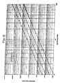
- FIG. 3 illustrates the electrostatic pressure acting on a dielectric substrate for different applied voltages with an electrostatic clamp 10 having electrode line widths of 10 ⁇ m.
- an electrostatic pressure of almost 4 Torr can be created by application of only 1000 volts to an electrostatic clamp with a spacing between electrodes of 200 ⁇ m.
- the voltage required to create a desired clamping force can be progressively decreased by decreasing the spacing between the electrodes to 100 ⁇ m, 50 ⁇ m and 20 ⁇ m, as shown in FIG. 3.
- the voltages required to operate the electrostatic clamp 10 may be still further reduced by decreasing the spacing between electrodes from 40 ⁇ m to 20 ⁇ m, 10 ⁇ m or 5 ⁇ m, as shown in FIG. 4.
- electrostatic clamps can be greatly increased by electrode lines and spaces which are substantially smaller than conventional electrostatic clamps.
- conventional manufacturing methods can only produce electrode lines and spaces which are no less than several hundred microns wide.
- manufacture of electrostatic clamps with small electrode line widths and spacings is further complicated by the requirements in a vacuum processing chamber for vacuum compatibility, high holding forces, good thermal conductivity, and excellent mechanical abrasion resistance.
- the electrostatic clamp 10 of the present invention can be manufactured by flat panel display (AMLCD) manufacturing technology.
- a suitable method of making the electrostatic clamp according to the present invention includes providing a dielectric substrate or base 12 on which the electrodes 14 are formed by pattern micro-lithography and etching using technologies which are generally used AMLCD manufacturing.
- the electrostatic clamp 10 includes a base 12 which is preferably formed of glass or quartz.
- the metal electrodes 14 are formed on the base 12 in a manner which will be described in more detail below.
- the electrodes 14 are preferably formed of electrically conductive material such as aluminum or polysilicon. However, the electrodes may also be formed of other materials commonly used for electrodes such as Cr, Mo, indium-tin-oxide, or other less common metals.
- the electrodes 14 are covered with an electrically insulating film 24 which protects the electrodes from abrasion, chemical attack, electrical breakdown and separates the substrate to be processed from the electrodes.
- the insulating film 24 is preferably formed of PECVD nitride such as silicon nitride, silicon dioxide, boron nitride, aluminum oxide, or combinations thereof. However, other insulating materials, such as SiO 2 or Si 3 N 4 , may also be used.
- nitride as a preferred coating is selected because it gives the electrostatic clamp 10 an abrasion resistant upper surface which protects the electrodes 14, the nitride has a high dielectric constant which improves the clamping force applied to the workpiece, and the nitride has a high breakdown voltage.
- the electrostatic clamp 10 may be formed by the following sequence of steps: 1) providing a bare clean glass substrate of an appropriate size; 2) deposit a thin metal film on the substrate by sputtering; 3) coat the thin metal film with photo-resist; 4) expose the photo-resist to ultraviolet light through a mask having a desired pattern and subsequently remove unexposed resist; 5) plasma or wet-chemical etch exposed metal, leaving behind an electrode array pattern; 6) strip remaining photo-resist from electrode pattern; 7) coat the electrode pattern with an electrically insulating film: and 8) connect alternating electrodes to electrical contacts.
- This process by which the electrostatic clamp according to the present invention may be manufactured is set forth by way of example only and is not intended as a limitation.
- the variations on the method preferably include the use of micro-lithographic technology for patterning the electrodes in the form of a thin film, and the use of thin film deposition and etching technologies for formation of the electrode and coating layers.
- the holding force of the electrostatic clamp according to the present invention increases as 1) the electrode line widths are reduced; 2) the spaces between the electrode lines are reduced; and 3) the coating layers are made thinner.
- electrode line widths and spacings of tens of microns result in acceptable clamping forces at lens or hundreds of volts rather than thousands of volts.
- FIG. 7 illustrates the effect of applied voltage on the performance of electrostatic clamp having electrodes with line widths of 10 ⁇ m, line spacings of 10 ⁇ m, and an insulating nitride coating of 1 ⁇ m.
- the two plots shown in FIG. 7 represent two different embodiments of the present invention having insulating coatings with dielectric constants of 6 and 9. As can be seen in the graph, the higher dielectric constant provides a higher clamping force for the same voltage.
Landscapes
- Physics & Mathematics (AREA)
- General Physics & Mathematics (AREA)
- Engineering & Computer Science (AREA)
- Condensed Matter Physics & Semiconductors (AREA)
- Manufacturing & Machinery (AREA)
- Computer Hardware Design (AREA)
- Microelectronics & Electronic Packaging (AREA)
- Power Engineering (AREA)
- Container, Conveyance, Adherence, Positioning, Of Wafer (AREA)
Abstract
Description
- The present invention relates to an electrostatic clamp for holding substrates in a vacuum processing chamber, and more particularly, the present invention relates to a low voltage electrostatic clamp for clamping dielectric substrates.
- Vacuum processing chambers are generally used for etching and chemical vapor depositing (CVD) of materials on substrates by supplying an etching or deposition gas to the vacuum chamber and application of an RF field to the gas. Examples of parallel plate, transformer coupled plasma (TCP), and electron-cyclotron resonance (ECR) reactors are disclosed in commonly owned U.S. Patent Nos. 4,340,462; 4,948,458; and 5,200,232. The substrates are held in place within the vacuum chamber during processing by substrate holders. Conventional substrate holders include mechanical clamps and electrostatic clamps (ESC). Examples of mechanical clamps and ESC substrate holders are provided in commonly owned U.S. Patent No. 5,262,029.
- Substrate holders in the form of an electrode can supply radiofrequency (RF) power into the chamber, as disclosed in U.S. Patent No. 4,579,618.
- Mechanical clamps generally employ a clamp ring which surrounds the substrate and presses down on the top surface of the substrate around its periphery. Further examples of mechanical clamping rings are disclosed in U.S. Patent Nos. 4,615,755; 5,013,400; and 5,326,725. Due to the fact that these known mechanical clamps cover the edge portions of the substrate, mechanical clamps reduce the area of the substrate which is able to be processed. Some additional drawbacks of mechanical clamps are that the clamp ring may cause damage to the edge of the substrate or may cause particles to become dislodged and contaminate the substrate in the chamber. Although mechanical clamps are suitable for use in many applications with small substrates, when large substrates such as flat panel displays are processed using mechanical clamps, the panels may have a tendency to become bowed due to the supply of pressurized gas used for increasing thermal conduction between the substrate and the water cooled substrate holder.
- Substrates used to make flat panel displays may have dimensions of about 320mm x 340mm, 360mm x 465mm, or as large as 600mm x 720mm with thicknesses of 0.7mm or 1.1mm and such substrates can be used for lap top computer screens. A discussion of flat panel display processing can be found in an article by Y. Kuo entitled "Reactive ion etching technology in thin-film-transistor processing," IBM J. Res. Develop., V. 36, No. 1, January 1992. In the past, these large flat panel display substrates have been held in place in processing chambers by the use of mechanical clamps. However, mechanical clamps have the disadvantages discussed above.
- Substrates including flat panel displays and smaller substrates can be cooled by the substrate holder during certain processing steps. Such cooling is performed by the application of an inert gas, such as helium, between the substrate holder and the opposed surface of the substrate. For instance, see U.S. Patent Nos. 5,160,152; 5,238,499; 5,350,479; and 5,534,816. The cooling gas typically fills channels or a pattern of grooves in the substrate holder and applies a back pressure to the substrate which tends to cause the substrate to become bowed upward at the center when the substrate is held only along the edges by a mechanical clamping apparatus. This bowing effect is even more pronounced for large substrates such as the type used to make flat panel displays. The bowing of the panel is undesirable since it causes non-uniform heat transfer to the substrate holder thus adversely affecting the processing of the panel.
- Electrostatic chucks are used for holding semiconducting and conducting substrates in place in a vacuum chamber in situations where it is desirable to avoid a clamping ring which extends over a portion of the substrate upper surface. Electrostatic chucks of the monopolar type utilize a single electrode. For instance, see U.S. Patent No. 4,665,463. Electrostatic chucks of the bipolar type utilize mutual attraction between two electrically charged capacitor plates which are separated by a dielectric layer. For instance, see U.S. Patent Nos. 4,692,836 and 5,055,964. An electrostatic chuck generally comprises an electrode with a dielectric layer formed on the electrode. A substrate of conductive or semiconductive material which is placed on the dielectric layer is attracted toward the electrode. Although this electrostatic attraction can be obtained between semiconducting and conducting substrates and an electrostatic chuck, this type of electrostatic attraction cannot be obtained with dielectric materials. With respect to conducting and semiconducting substrates, electrostatic chucks are beneficial because they exert a holding force on the entire substrate which counteracts the force of the cooling gas applied to the back of the substrate and does not cause the substrate to bow or warp.
- The benefits of an electrostatic chuck would be highly desirable for use with flat panel displays. However, because flat panel displays are generally made of non-conductive materials, such as glass, conventional electrostatic chucks cannot be used.
- The device according to the present invention addresses the disadvantages of the prior art by providing an electrostatic clamp which may be used for dielectric substrates. The electrostatic clamp can be used in a variety of manufacturing processes such as etching, plasma CVD, thermal CVD, RTP, implantation, sputtering, resist stripping, resist coating, lithograph, substrate handling, etc. The electrostatic clamp according to the present invention operates at low voltages thereby avoiding problems associated with high voltage ESC systems.
- US-A-5,315,473 describes an electrostatic clamp or, chuck usable for clamping conductors and semiconductors which takes the form of an array of spaced apart electrically conductive strips acting as electrodes on a dielectric base. The electrodes are arranged in first and second groups with the electrodes of each group alternating with respect to the other electrodes. The first and second groups of electrodes are connected to an a.c. voltage source.
- EP-A-0506537 also describes an electrostatic clamp with a pair of electrodes in the form of spaced apart layers of electrically conductive material.
- According to the invention there is provided an electrostatic clamp for clamping dielectric substrates comprising:
- an array of spaced-apart and electrically conductive electrodes formed on a dielectric base wherein the width of each of the electrodes in the array of electrodes is less than 100 µm and the spacing between the electrodes is less than 100 µm;
- a first electrical contact connected to a first voltage source connected to a first group of the electrodes and a second electrical contact connected to a second voltage source connected to a second group of the electrodes, the first and second groups of electrodes oppositely alternating with respect to each other in the array of electrodes wherein the first and second voltage sources are of opposite polarity and cause the first and second groups of electrodes to create a non-uniform electric field.
-
- The first and second sources serve to apply voltages of opposite polarity and magnitudes of less than 1 kV to the first and second electrical contacts, wherein the electrode width and spacing is small enough that less than 1 kV applied to the first and second electrical contacts provides a sufficient clamping force to clamp a dielectric substrate while opposing an opposite force of at least 2 Torr of backside pressure.
- According to an embodiment of the invention, there is provided a method of making an electrostatic clamp comprising:
- depositing a thin metal film on a dielectric substrate;
- forming an array of electrodes by etching the thin metal film by micro-lithography, wherein the electrodes which are formed by the etching have widths of less than 100 µm, and spacings between the electrodes are less than 100 µm;
- coating the electrodes with an electrically insulating film; and
- connecting common electrical contacts to alternating electrodes in the array of electrodes.
-
- According to another embodiment of the invention, there is provided a method of processing a substrate in a process chamber having an electrostatic clamp hereinbefore described for supporting the substrate during processing thereof, the method comprising:
- supplying a substrate to the process chamber at a position above the electrostatic clamp;
- clamping the substrate by supplying voltage to the first and second groups of electrodes of the clamp to electrostatically attract the substrate against the upper surface of the clamp; and
- processing an exposed surface of the substrate.
-
- The process can further include supplying a heat transfer gas between the lower surface of the substrate and the upper surface of the clamp. For instance, the upper surface of the substrate can be etched or coated during the processing step The process chamber can be part of an ECR reactor, TCP reactor or parallel plate reactor. The clamp can be a bipolar electrostatic chuck and the substrate can be a glass panel suitable for use in making a flat panel display or a semiconductor wafer. The clamp can be supplied DC voltage of 50 to 1000 volts during the clamping step. In order to cool the substrate, helium gas can be supplied to a space between the lower surface of the substrate and the upper surface of the clamp by passing the helium through one or more channels in the clamp.
- The invention will be described in greater detail with reference to the accompanying drawings in which like elements bear like reference numerals, and wherein:
- FIG. I is a top view of an electrostatic clamp according to the present invention wherein electrode lines are enlarged for clarity;
- FIG. 2 is a cross-sectional side view of the electrostatic clamp taken along line 2-2 of FIG. 1;
- FIG. 3 is a graph of the electrostatic pressure in Torr versus applied
voltage in volts for an electrostatic clamp according to the present invention
having 10 µm wide electrode lines and spaces between the electrodes of 20, 50,
100, and
200 µm; - FIG. 4 is a graph of electrostatic pressure in Torr versus applied voltage in volts for an electrostatic clamp according to the present invention having 10 µm wide electrode lines and spaces between the electrodes of 5, 10, 20, and 40 µm;
- FIG. 5 is an enlarged side view of an electrostatic clamp showing the electric fields created;
- FIG. 6 is an enlarged side sectional view of the electrostatic clamp according to the present invention; and
- FIG. 7 is a graph of the effect of applied voltage on electrostatic clamp performance for two variations of the present invention.
-
- The present invention provides an
electrostatic clamp 10 as shown in FIGS. 1 and 2 which can be used to clamp substrates such as large dielectric substrates within a processing chamber such as a vacuum chamber. Dielectric objects can be electrostatically clamped by immersing the dielectric object in a non-uniform electric field. The non-uniform electric field produces a force which tends to pull the dielectric object into the region of the highest electric field. - The
electrostatic clamp 10 according to the present invention includes abase 12 of dielectric material such as glass, alumina, etc., on which a plurality ofelectrodes 14 of electrically conductive material such as aluminum, copper, tungsten, etc., are formed as spaced-apart lines on the base. Preferably, the pattern of theelectrodes 14 formed on thebase 12 is an interdigitated pattern of two sets of alternating parallel conductor lines. However, other electrode patterns, such as a concentric circular pattern or an irregular pattern can also be used. The pattern may be interrupted by lifter pin holes (not shown) or other features which may be located on the surface of theelectrostatic clamp 10. To provide power of opposite polarity to the two sets of conductor lines,electrical connectors electrostatic clamp 10. Alternatingelectrodes 14 in the electrode array are connected to oneelectrical contact 16, while opposite alternating electrodes are connected to the other of theelectrical contacts 18. - As shown in FIG. 5,
adjacent electrodes 14 are oppositely charged by one or more voltage sources connected to theelectrical contacts electric field 20 abovedielectric coating 24. The non-uniformelectric field 20 causes adielectric workpiece 22 which is placed on thedielectric coating 24 of theelectrostatic clamp 10 to be pulled toward the region of the highest electric field. The region of highest electric field is generally located between the oppositely charged electrodes. - Conventional electrostatic clamps used for clamping semiconducting or conducting substrates such as silicon wafers include spaced-apart electrode lines with line widths of approximately 3 mm and spacings between lines of approximately 1 mm. If such an electrostatic clamp was used to hold a dielectric substrate, the voltage required to create the necessary clamping force which overcomes the backside pressure applied by the cooling gas would be approximately 5000 volts.
- The attractive force generated by known electrostatic clamps on a dielectric workpiece is relatively weak, since conventional manufacturing methods produce electrode lines and spaces between electrode lines which are no less than several hundred microns wide. With such arrangements, thousands of volts are required to hold a dielectric substrate 22 (such as the type used to produce flat panel displays) with the several Torr required to hold the substrate securely on the
electrostatic clamp 10. These high voltages are undesirable for a number of reasons including, safety concerns, potential damage to devices being processed on the substrate, added design complexity, high power consumption and high costs associated with design of the electrostatic clamp and electrical circuits capable of delivering and handling the high voltages. High voltages are also undesirable due to the potential to cause arcing or other malfunctions as a result of irregularities in the electrostatic clamp or the processing system. - FIG. 3 illustrates the electrostatic pressure acting on a dielectric substrate for different applied voltages with an
electrostatic clamp 10 having electrode line widths of 10 µm. As shown in FIG. 3, when the line width is reduced to 10 µm, an electrostatic pressure of almost 4 Torr can be created by application of only 1000 volts to an electrostatic clamp with a spacing between electrodes of 200 µm. The voltage required to create a desired clamping force can be progressively decreased by decreasing the spacing between the electrodes to 100 µm, 50 µm and 20 µm, as shown in FIG. 3. The voltages required to operate theelectrostatic clamp 10 may be still further reduced by decreasing the spacing between electrodes from 40 µm to 20 µm, 10 µm or 5 µm, as shown in FIG. 4. - As explained above, the attractive force generated by electrostatic clamps can be greatly increased by electrode lines and spaces which are substantially smaller than conventional electrostatic clamps. However, conventional manufacturing methods can only produce electrode lines and spaces which are no less than several hundred microns wide. Thus, there is a need in the art for a process capable of providing electrostatic clamps having a large number of closely spaced conductor lines while minimizing the expense of making such lines on a large scale such that the clamp can be used for clamping large dielectric substrates such as flat panel displays. It should be noted, however, that manufacture of electrostatic clamps with small electrode line widths and spacings is further complicated by the requirements in a vacuum processing chamber for vacuum compatibility, high holding forces, good thermal conductivity, and excellent mechanical abrasion resistance.
- Semiconductor wafer processing technology is unsuitable for manufacturing devices having dielectric substrates. Thus, in order to achieve extremely small electrode lines with very close spacing over a large area with plasma-compatible materials on a dielectric substrate or base, the
electrostatic clamp 10 of the present invention can be manufactured by flat panel display (AMLCD) manufacturing technology. A suitable method of making the electrostatic clamp according to the present invention includes providing a dielectric substrate orbase 12 on which theelectrodes 14 are formed by pattern micro-lithography and etching using technologies which are generally used AMLCD manufacturing. - An enlarged cross-sectional view of a portion of an
electrostatic clamp 10 according to the present invention is shown by way of example in FIG. 6. Theelectrostatic clamp 10 includes a base 12 which is preferably formed of glass or quartz. Themetal electrodes 14 are formed on the base 12 in a manner which will be described in more detail below. Theelectrodes 14 are preferably formed of electrically conductive material such as aluminum or polysilicon. However, the electrodes may also be formed of other materials commonly used for electrodes such as Cr, Mo, indium-tin-oxide, or other less common metals. Theelectrodes 14 are covered with an electrically insulatingfilm 24 which protects the electrodes from abrasion, chemical attack, electrical breakdown and separates the substrate to be processed from the electrodes. The insulatingfilm 24 is preferably formed of PECVD nitride such as silicon nitride, silicon dioxide, boron nitride, aluminum oxide, or combinations thereof. However, other insulating materials, such as SiO2 or Si3N4, may also be used. The use of nitride as a preferred coating is selected because it gives theelectrostatic clamp 10 an abrasion resistant upper surface which protects theelectrodes 14, the nitride has a high dielectric constant which improves the clamping force applied to the workpiece, and the nitride has a high breakdown voltage. - The
electrostatic clamp 10 according to the present invention may be formed by the following sequence of steps: 1) providing a bare clean glass substrate of an appropriate size; 2) deposit a thin metal film on the substrate by sputtering; 3) coat the thin metal film with photo-resist; 4) expose the photo-resist to ultraviolet light through a mask having a desired pattern and subsequently remove unexposed resist; 5) plasma or wet-chemical etch exposed metal, leaving behind an electrode array pattern; 6) strip remaining photo-resist from electrode pattern; 7) coat the electrode pattern with an electrically insulating film: and 8) connect alternating electrodes to electrical contacts. This process by which the electrostatic clamp according to the present invention may be manufactured is set forth by way of example only and is not intended as a limitation. - There are many variations on this process using flat panel display manufacturing methods. However, the variations on the method preferably include the use of micro-lithographic technology for patterning the electrodes in the form of a thin film, and the use of thin film deposition and etching technologies for formation of the electrode and coating layers.
- The holding force of the electrostatic clamp according to the present invention increases as 1) the electrode line widths are reduced; 2) the spaces between the electrode lines are reduced; and 3) the coating layers are made thinner. As shown in FIGS. 3 and 4, electrode line widths and spacings of tens of microns result in acceptable clamping forces at lens or hundreds of volts rather than thousands of volts.
- The pressure exerted by the
electrostatic clamp 10 is also affected by the dielectric constant of the insulating coating. FIG. 7 illustrates the effect of applied voltage on the performance of electrostatic clamp having electrodes with line widths of 10 µm, line spacings of 10 µm, and an insulating nitride coating of 1 µm. The two plots shown in FIG. 7 represent two different embodiments of the present invention having insulating coatings with dielectric constants of 6 and 9. As can be seen in the graph, the higher dielectric constant provides a higher clamping force for the same voltage.
Claims (18)
- An electrostatic clamp (10) for clamping dielectric substrates comprising:an array of spaced-apart and electrically conductive electrodes (14) formed on a dielectric base (12) wherein the width of each of the electrodes in the array of electrodes is less than 100 µm and the spacing between the electrodes is less than 100 µm;a first electrical contact (16) connected to a first voltage source connected to a first group of the electrodes and a second electrical contact (18) connected to a second voltage source connected to a second group of the electrodes, the first and second groups of electrodes oppositely alternating with respect to each other in the array of electrodes wherein the first and second voltage sources are of opposite polarity and cause the first and second groups of electrodes to create a non-uniform electric field.
- The electrostatic clamp according to claim 1 wherein the width of the electrodes is less than 50 µm and the spacing between the electrodes is less than 50 µm.
- The electrostatic clamp according to claim 1 wherein the spacing between the electrodes is 5 to 20 µm and the width of the electrodes is 5 to 20 µm.
- The electrostatic clamp according to any one of the preceding claims wherein the array of electrodes is covered with a dielectric insulating layer (24).
- The electrostatic clamp according to claim 4 wherein the insulating layer is formed of silicon nitride, silicon oxide, aluminium oxide, boron nitride or combinations thereof.
- The electrostatic clamp according to claim 4 or 5 wherein the insulating layer has a thickness of less than 10 µm.
- An electrostatic clamp according to any one of the preceding claims wherein the first and second voltage sources serve to voltages of opposite polarity and magnitude of less than I kV to the first and second electrical contacts respectively, wherein the electrode width and spacing is small enough that voltages of opposite polarity and magnitude less than 1 kV applied to the first and second electrical contacts provides a sufficient clamping force to clamp a dielectric substrate against at least 2 Torr of backside pressure.
- A method of making an electrostatic clamp according to claim 1 comprising:depositing a thin metal film on a dielectric substrate;forming an array of electrodes by etching the thin metal film by micro-lithography, wherein the electrodes which are formed by the etching have widths of less than 100 µm, and spacings between the electrodes are less than 100 µm;coating the electrodes with an electrically insulating film; andconnecting common electrical contacts to alternating electrodes in the array of electrodes.
- The method of claim 8 wherein the step of depositing the thin metal film includes depositing the thin metal film by sputtering.
- The method of claim 8 or claim 9 wherein the step of etching the thin metal film comprises:coating the thin metal film with photo-resist;exposing the photo-resist through a mask;removing the unexposed photo-resist so as to provide exposed metal portions of the metal film; andetching the exposed metal portions so as to form the array of electrodes from the remainder of the metal film.
- A method of processing a substrate in a process chamber having an electrostatic clamp as claimed in any one of claims 1 to 7 for supporting the substrate during processing thereof, the method comprising:supplying a substrate to the process chamber at a position above the electrostatic clamp;clamping the substrate by supplying voltage to the first and second groups of the electrodes of the clamp to electrostatically attract the substrate against the upper surface of the clamp; andprocessing an exposed surface of the substrate.
- The method of claim 11 wherein the groups of electrodes are each supplied with a DC voltage of magnitude less than 1000 volts during the clamping step.
- The method of claim 11 or 12 wherein helium gas is supplied to a space between the lower surface of the substrate and the upper surface of the clamp by passing the helium through one or more channels in the clamp.
- The method of claim 12 further comprising supplying a heat transfer gas between the lower surface of the substrate and the upper surface of the clamp.
- The method of claim 12 wherein the upper surface of the substrate is etched in a plasma environment during the processing step.
- The method of claim 12 wherein the upper surface of the substrate is coated in a plasma environment during the processing step.
- The method of claim 12 wherein the clamp is a bipolar electrostatic chuck and the substrate is a glass panel suitable for use in making a flat panel display.
- The method of claim 12 wherein the clamp is a bipolar electrostatic chuck and the substrate is a semiconductor wafer.
Applications Claiming Priority (3)
| Application Number | Priority Date | Filing Date | Title |
|---|---|---|---|
| US08/577,382 US5838529A (en) | 1995-12-22 | 1995-12-22 | Low voltage electrostatic clamp for substrates such as dielectric substrates |
| US577382 | 1995-12-22 | ||
| PCT/US1996/020883 WO1997023945A1 (en) | 1995-12-22 | 1996-12-20 | Low voltage electrostatic clamp for substrates such as dielectric substrates |
Publications (2)
| Publication Number | Publication Date |
|---|---|
| EP0880818A1 EP0880818A1 (en) | 1998-12-02 |
| EP0880818B1 true EP0880818B1 (en) | 2003-02-26 |
Family
ID=24308464
Family Applications (1)
| Application Number | Title | Priority Date | Filing Date |
|---|---|---|---|
| EP96945445A Expired - Lifetime EP0880818B1 (en) | 1995-12-22 | 1996-12-20 | Low voltage electrostatic clamp for substrates such as dielectric substrates |
Country Status (4)
| Country | Link |
|---|---|
| US (1) | US5838529A (en) |
| EP (1) | EP0880818B1 (en) |
| JP (1) | JP3941966B2 (en) |
| WO (1) | WO1997023945A1 (en) |
Families Citing this family (61)
| Publication number | Priority date | Publication date | Assignee | Title |
|---|---|---|---|---|
| US6669653B2 (en) * | 1997-05-05 | 2003-12-30 | Trig Medical Ltd. | Method and apparatus for monitoring the progress of labor |
| JP3805134B2 (en) * | 1999-05-25 | 2006-08-02 | 東陶機器株式会社 | Electrostatic chuck for insulating substrate adsorption |
| US6444083B1 (en) | 1999-06-30 | 2002-09-03 | Lam Research Corporation | Corrosion resistant component of semiconductor processing equipment and method of manufacturing thereof |
| US6227140B1 (en) | 1999-09-23 | 2001-05-08 | Lam Research Corporation | Semiconductor processing equipment having radiant heated ceramic liner |
| US6408786B1 (en) | 1999-09-23 | 2002-06-25 | Lam Research Corporation | Semiconductor processing equipment having tiled ceramic liner |
| US6673198B1 (en) * | 1999-12-22 | 2004-01-06 | Lam Research Corporation | Semiconductor processing equipment having improved process drift control |
| JP4640876B2 (en) * | 2000-06-13 | 2011-03-02 | 株式会社アルバック | Substrate transfer device |
| CN1258256C (en) * | 2000-06-14 | 2006-05-31 | 赫尔曼·阿莉森 | Electro-adhesion device |
| US6890861B1 (en) | 2000-06-30 | 2005-05-10 | Lam Research Corporation | Semiconductor processing equipment having improved particle performance |
| US6506254B1 (en) | 2000-06-30 | 2003-01-14 | Lam Research Corporation | Semiconductor processing equipment having improved particle performance |
| US6475336B1 (en) | 2000-10-06 | 2002-11-05 | Lam Research Corporation | Electrostatically clamped edge ring for plasma processing |
| US6613442B2 (en) | 2000-12-29 | 2003-09-02 | Lam Research Corporation | Boron nitride/yttria composite components of semiconductor processing equipment and method of manufacturing thereof |
| US7128804B2 (en) * | 2000-12-29 | 2006-10-31 | Lam Research Corporation | Corrosion resistant component of semiconductor processing equipment and method of manufacture thereof |
| US6537429B2 (en) | 2000-12-29 | 2003-03-25 | Lam Research Corporation | Diamond coatings on reactor wall and method of manufacturing thereof |
| US6533910B2 (en) | 2000-12-29 | 2003-03-18 | Lam Research Corporation | Carbonitride coated component of semiconductor processing equipment and method of manufacturing thereof |
| US6620520B2 (en) * | 2000-12-29 | 2003-09-16 | Lam Research Corporation | Zirconia toughened ceramic components and coatings in semiconductor processing equipment and method of manufacture thereof |
| US6790242B2 (en) | 2000-12-29 | 2004-09-14 | Lam Research Corporation | Fullerene coated component of semiconductor processing equipment and method of manufacturing thereof |
| US6830622B2 (en) * | 2001-03-30 | 2004-12-14 | Lam Research Corporation | Cerium oxide containing ceramic components and coatings in semiconductor processing equipment and methods of manufacture thereof |
| US6483690B1 (en) | 2001-06-28 | 2002-11-19 | Lam Research Corporation | Ceramic electrostatic chuck assembly and method of making |
| US6780787B2 (en) | 2002-03-21 | 2004-08-24 | Lam Research Corporation | Low contamination components for semiconductor processing apparatus and methods for making components |
| US7311797B2 (en) * | 2002-06-27 | 2007-12-25 | Lam Research Corporation | Productivity enhancing thermal sprayed yttria-containing coating for plasma reactor |
| US6898065B2 (en) * | 2002-07-26 | 2005-05-24 | Brad Mays | Method and apparatus for operating an electrostatic chuck in a semiconductor substrate processing system |
| US7033443B2 (en) * | 2003-03-28 | 2006-04-25 | Axcelis Technologies, Inc. | Gas-cooled clamp for RTP |
| JP4247739B2 (en) * | 2003-07-09 | 2009-04-02 | Toto株式会社 | Method of attracting glass substrate by electrostatic chuck and electrostatic chuck |
| EP1498780A3 (en) * | 2003-07-15 | 2005-04-06 | ASML Netherlands B.V. | Substrate holder and lithographic projection apparatus |
| EP1498777A1 (en) * | 2003-07-15 | 2005-01-19 | ASML Netherlands B.V. | Substrate holder and lithographic projection apparatus |
| US7072165B2 (en) * | 2003-08-18 | 2006-07-04 | Axcelis Technologies, Inc. | MEMS based multi-polar electrostatic chuck |
| US6947274B2 (en) * | 2003-09-08 | 2005-09-20 | Axcelis Technologies, Inc. | Clamping and de-clamping semiconductor wafers on an electrostatic chuck using wafer inertial confinement by applying a single-phase square wave AC clamping voltage |
| US7072166B2 (en) * | 2003-09-12 | 2006-07-04 | Axcelis Technologies, Inc. | Clamping and de-clamping semiconductor wafers on a J-R electrostatic chuck having a micromachined surface by using force delay in applying a single-phase square wave AC clamping voltage |
| US6905984B2 (en) * | 2003-10-10 | 2005-06-14 | Axcelis Technologies, Inc. | MEMS based contact conductivity electrostatic chuck |
| US6946403B2 (en) * | 2003-10-28 | 2005-09-20 | Axcelis Technologies, Inc. | Method of making a MEMS electrostatic chuck |
| US7245357B2 (en) * | 2003-12-15 | 2007-07-17 | Asml Netherlands B.V. | Lithographic apparatus and device manufacturing method |
| KR100526923B1 (en) * | 2004-01-05 | 2005-11-09 | 삼성전자주식회사 | Manufactureing method and lift pin of semiconductor production device therefor |
| WO2005091356A1 (en) | 2004-03-19 | 2005-09-29 | Creative Technology Corporation | Bipolar electrostatic chuck |
| TWI271815B (en) | 2004-11-30 | 2007-01-21 | Sanyo Electric Co | Method for processing stuck object and electrostatic sticking method |
| EP1909308B1 (en) | 2005-07-08 | 2013-02-27 | Creative Technology Corporation | Electrode sheet for electrostatic chuck |
| DE202005011367U1 (en) | 2005-07-18 | 2005-09-29 | Retzlaff, Udo, Dr. | Transfer-ESC for moving ultra-thin chips during manufacture has a base material wafer with a multiplicity of grouped electrode cells each with an electrode tip, insulator, outer electrode cover and dielectric cover |
| US20070139855A1 (en) * | 2005-12-21 | 2007-06-21 | Asml Netherlands B.V. | Lithographic apparatus and method of manufacturing an electrostatic clamp for a lithographic apparatus |
| CN101416031A (en) * | 2006-03-29 | 2009-04-22 | 约翰尼斯海登海恩博士股份有限公司 | Method for holding a scale on a carrier and arrangement having a carrier and a scale |
| US20080151466A1 (en) * | 2006-12-26 | 2008-06-26 | Saint-Gobain Ceramics & Plastics, Inc. | Electrostatic chuck and method of forming |
| WO2008082978A2 (en) | 2006-12-26 | 2008-07-10 | Saint-Gobain Ceramics & Plastics, Inc. | Electrostatic chuck and method of forming |
| KR100886015B1 (en) | 2007-05-15 | 2009-02-26 | 삼성전자주식회사 | Dry cleaning method of semiconductor production device having muti-lifter |
| US7972471B2 (en) * | 2007-06-29 | 2011-07-05 | Lam Research Corporation | Inductively coupled dual zone processing chamber with single planar antenna |
| KR101553423B1 (en) | 2007-12-19 | 2015-09-15 | 램 리써치 코포레이션 | Film adhesive for semiconductor vacuum processing apparatus |
| CN101903979B (en) * | 2007-12-19 | 2012-02-01 | 朗姆研究公司 | Composite showerhead electrode assembly, method for connecting members thereof, and substrate processing method |
| JP2008205509A (en) * | 2008-05-15 | 2008-09-04 | Ulvac Japan Ltd | Method for carrying insulating substrate, and alignment method |
| JP2008205508A (en) * | 2008-05-15 | 2008-09-04 | Ulvac Japan Ltd | Substrate carrier, and vacuum processing apparatus |
| US7760004B2 (en) * | 2008-10-30 | 2010-07-20 | Analog Devices, Inc. | Clamp networks to insure operation of integrated circuit chips |
| JP6085616B2 (en) | 2012-02-03 | 2017-02-22 | エーエスエムエル ネザーランズ ビー.ブイ. | Substrate holder, lithographic apparatus, device manufacturing method, and substrate holder manufacturing method |
| GB201321463D0 (en) | 2013-12-05 | 2014-01-22 | Oxford Instr Nanotechnology Tools Ltd | Electrostatic clamping method and apparatus |
| CN105812989A (en) * | 2014-12-31 | 2016-07-27 | 鸿富锦精密工业(深圳)有限公司 | Loudspeaker |
| FR3063832B1 (en) | 2017-03-08 | 2019-03-22 | Commissariat A L'energie Atomique Et Aux Energies Alternatives | METHOD OF SELF-ASSEMBLING MICROELECTRONIC COMPONENTS |
| DE102019101657A1 (en) | 2019-01-23 | 2020-07-23 | Berliner Glas Kgaa Herbert Kubatz Gmbh & Co | Holding device for electrostatically holding a component with a base body joined by diffusion bonding and method for its production |
| CN113795473A (en) | 2019-04-05 | 2021-12-14 | 贺利氏科纳米北美有限责任公司 | Controlled porosity yttria for etch applications |
| EP4222129A1 (en) | 2020-10-03 | 2023-08-09 | Heraeus Conamic North America LLC | Sintered yttrium oxide body of large dimension |
| US20240158301A1 (en) | 2020-10-15 | 2024-05-16 | Heraeus Conamic North America Llc | Multilayer sintered ceramic body and method of making |
| KR20230104668A (en) | 2020-12-18 | 2023-07-10 | 헤레우스 코나믹 노스 아메리카 엘엘씨 | multi-layer sintered ceramic body |
| WO2023122597A1 (en) | 2021-12-23 | 2023-06-29 | Heraeus Conamic North America Llc | Multilayer sintered ceramic body and method of making |
| EP4215360A1 (en) | 2022-01-24 | 2023-07-26 | Heraeus Conamic North America LLC | Multilayer sintered ceramic body and method of making |
| TW202340123A (en) | 2022-03-31 | 2023-10-16 | 美商賀利氏科納米北美有限責任公司 | High frequency polishing of ceramics |
| EP4269024A1 (en) | 2022-04-29 | 2023-11-01 | Heraeus Conamic North America LLC | High frequency polishing of ceramics |
Family Cites Families (29)
| Publication number | Priority date | Publication date | Assignee | Title |
|---|---|---|---|---|
| US3634740A (en) * | 1970-04-20 | 1972-01-11 | Addressograph Multigraph | Electrostatic holddown |
| US3916270A (en) * | 1974-05-02 | 1975-10-28 | Tektronix Inc | Electrostatic holddown apparatus |
| US4184188A (en) * | 1978-01-16 | 1980-01-15 | Veeco Instruments Inc. | Substrate clamping technique in IC fabrication processes |
| US4384918A (en) * | 1980-09-30 | 1983-05-24 | Fujitsu Limited | Method and apparatus for dry etching and electrostatic chucking device used therein |
| US4340462A (en) * | 1981-02-13 | 1982-07-20 | Lam Research Corporation | Adjustable electrode plasma processing chamber |
| GB2106325A (en) * | 1981-09-14 | 1983-04-07 | Philips Electronic Associated | Electrostatic chuck |
| JPS6059104B2 (en) * | 1982-02-03 | 1985-12-23 | 株式会社東芝 | electrostatic chuck board |
| US4551192A (en) * | 1983-06-30 | 1985-11-05 | International Business Machines Corporation | Electrostatic or vacuum pinchuck formed with microcircuit lithography |
| GB2147459A (en) * | 1983-09-30 | 1985-05-09 | Philips Electronic Associated | Electrostatic chuck for semiconductor wafers |
| US4692836A (en) * | 1983-10-31 | 1987-09-08 | Toshiba Kikai Kabushiki Kaisha | Electrostatic chucks |
| US4579618A (en) * | 1984-01-06 | 1986-04-01 | Tegal Corporation | Plasma reactor apparatus |
| US4534816A (en) * | 1984-06-22 | 1985-08-13 | International Business Machines Corporation | Single wafer plasma etch reactor |
| US4615755A (en) * | 1985-08-07 | 1986-10-07 | The Perkin-Elmer Corporation | Wafer cooling and temperature control for a plasma etching system |
| US4724510A (en) * | 1986-12-12 | 1988-02-09 | Tegal Corporation | Electrostatic wafer clamp |
| US5262029A (en) * | 1988-05-23 | 1993-11-16 | Lam Research | Method and system for clamping semiconductor wafers |
| US4962441A (en) * | 1989-04-10 | 1990-10-09 | Applied Materials, Inc. | Isolated electrostatic wafer blade clamp |
| US4948458A (en) * | 1989-08-14 | 1990-08-14 | Lam Research Corporation | Method and apparatus for producing magnetically-coupled planar plasma |
| US5001594A (en) * | 1989-09-06 | 1991-03-19 | Mcnc | Electrostatic handling device |
| US5013400A (en) * | 1990-01-30 | 1991-05-07 | General Signal Corporation | Dry etch process for forming champagne profiles, and dry etch apparatus |
| JP3129452B2 (en) * | 1990-03-13 | 2001-01-29 | 富士電機株式会社 | Electrostatic chuck |
| US5238499A (en) * | 1990-07-16 | 1993-08-24 | Novellus Systems, Inc. | Gas-based substrate protection during processing |
| US5055964A (en) * | 1990-09-07 | 1991-10-08 | International Business Machines Corporation | Electrostatic chuck having tapered electrodes |
| US5200232A (en) * | 1990-12-11 | 1993-04-06 | Lam Research Corporation | Reaction chamber design and method to minimize particle generation in chemical vapor deposition reactors |
| EP0506537A1 (en) * | 1991-03-28 | 1992-09-30 | Shin-Etsu Chemical Co., Ltd. | Electrostatic chuck |
| US5191506A (en) * | 1991-05-02 | 1993-03-02 | International Business Machines Corporation | Ceramic electrostatic chuck |
| US5155652A (en) * | 1991-05-02 | 1992-10-13 | International Business Machines Corporation | Temperature cycling ceramic electrostatic chuck |
| US5315473A (en) * | 1992-01-21 | 1994-05-24 | Applied Materials, Inc. | Isolated electrostatic chuck and excitation method |
| US5350479A (en) * | 1992-12-02 | 1994-09-27 | Applied Materials, Inc. | Electrostatic chuck for high power plasma processing |
| US5326725A (en) * | 1993-03-11 | 1994-07-05 | Applied Materials, Inc. | Clamping ring and susceptor therefor |
-
1995
- 1995-12-22 US US08/577,382 patent/US5838529A/en not_active Expired - Lifetime
-
1996
- 1996-12-20 WO PCT/US1996/020883 patent/WO1997023945A1/en active IP Right Grant
- 1996-12-20 EP EP96945445A patent/EP0880818B1/en not_active Expired - Lifetime
- 1996-12-20 JP JP52388897A patent/JP3941966B2/en not_active Expired - Lifetime
Also Published As
| Publication number | Publication date |
|---|---|
| JP2000502509A (en) | 2000-02-29 |
| JP3941966B2 (en) | 2007-07-11 |
| WO1997023945A1 (en) | 1997-07-03 |
| EP0880818A1 (en) | 1998-12-02 |
| US5838529A (en) | 1998-11-17 |
Similar Documents
| Publication | Publication Date | Title |
|---|---|---|
| EP0880818B1 (en) | Low voltage electrostatic clamp for substrates such as dielectric substrates | |
| WO1997023945A9 (en) | Low voltage electrostatic clamp for substrates such as dielectric substrates | |
| US5805408A (en) | Electrostatic clamp with lip seal for clamping substrates | |
| EP0049588B1 (en) | Method and apparatus for dry etching and electrostatic chucking device used therein | |
| US5847918A (en) | Electrostatic clamping method and apparatus for dielectric workpieces in vacuum processors | |
| KR100511854B1 (en) | Electrostatic chuck device | |
| EP0439000B1 (en) | Electrostatic clamp and method | |
| US5255153A (en) | Electrostatic chuck and plasma apparatus equipped therewith | |
| US4971667A (en) | Plasma processing method and apparatus | |
| KR100578281B1 (en) | Electrostatic support assembly having an integral ion focus ring | |
| US20140150246A1 (en) | Apparatus and Method for Carrying Substrates | |
| US8139340B2 (en) | Conductive seal ring electrostatic chuck | |
| US5606485A (en) | Electrostatic chuck having improved erosion resistance | |
| US7736462B2 (en) | Installation for processing a substrate | |
| US6117246A (en) | Conductive polymer pad for supporting a workpiece upon a workpiece support surface of an electrostatic chuck | |
| EP0693770A1 (en) | Electrostatic chuck for magnetic flux processing | |
| EP0346131A2 (en) | Dry etching apparatus | |
| EP0692814A1 (en) | Multi-electrode electrostatic chuck | |
| JPH1064989A (en) | Shield for electrostatic chuck | |
| JP2002151581A (en) | Method and apparatus for dechucking a substrate | |
| US5283087A (en) | Plasma processing method and apparatus | |
| US6935038B2 (en) | Gap gauge | |
| TWI440123B (en) | Apparatus and method for carrying substrates | |
| US8672311B2 (en) | Method of cooling textured workpieces with an electrostatic chuck | |
| Ogiya et al. | Study of substrate cooling mechanism of ICP dry etching system in non-silicon field |
Legal Events
| Date | Code | Title | Description |
|---|---|---|---|
| PUAI | Public reference made under article 153(3) epc to a published international application that has entered the european phase |
Free format text: ORIGINAL CODE: 0009012 |
|
| 17P | Request for examination filed |
Effective date: 19980714 |
|
| AK | Designated contracting states |
Kind code of ref document: A1 Designated state(s): GB |
|
| RIN1 | Information on inventor provided before grant (corrected) |
Inventor name: BARNES, MICHAEL, SCOTT Inventor name: SHUFFLEBOTHAM, PAUL, KEVIN |
|
| 17Q | First examination report despatched |
Effective date: 20001208 |
|
| GRAH | Despatch of communication of intention to grant a patent |
Free format text: ORIGINAL CODE: EPIDOS IGRA |
|
| GRAH | Despatch of communication of intention to grant a patent |
Free format text: ORIGINAL CODE: EPIDOS IGRA |
|
| GRAA | (expected) grant |
Free format text: ORIGINAL CODE: 0009210 |
|
| AK | Designated contracting states |
Designated state(s): GB |
|
| REG | Reference to a national code |
Ref country code: GB Ref legal event code: FG4D |
|
| PLBE | No opposition filed within time limit |
Free format text: ORIGINAL CODE: 0009261 |
|
| STAA | Information on the status of an ep patent application or granted ep patent |
Free format text: STATUS: NO OPPOSITION FILED WITHIN TIME LIMIT |
|
| 26N | No opposition filed |
Effective date: 20031127 |
|
| PGFP | Annual fee paid to national office [announced via postgrant information from national office to epo] |
Ref country code: GB Payment date: 20121227 Year of fee payment: 17 |
|
| GBPC | Gb: european patent ceased through non-payment of renewal fee |
Effective date: 20131220 |
|
| PG25 | Lapsed in a contracting state [announced via postgrant information from national office to epo] |
Ref country code: GB Free format text: LAPSE BECAUSE OF NON-PAYMENT OF DUE FEES Effective date: 20131220 |