EP0878833A2 - Process for the selective formation of salicide on active areas of MOS devices - Google Patents
Process for the selective formation of salicide on active areas of MOS devices Download PDFInfo
- Publication number
- EP0878833A2 EP0878833A2 EP98830235A EP98830235A EP0878833A2 EP 0878833 A2 EP0878833 A2 EP 0878833A2 EP 98830235 A EP98830235 A EP 98830235A EP 98830235 A EP98830235 A EP 98830235A EP 0878833 A2 EP0878833 A2 EP 0878833A2
- Authority
- EP
- European Patent Office
- Prior art keywords
- layer
- regions
- gate
- source
- sub
- Prior art date
- Legal status (The legal status is an assumption and is not a legal conclusion. Google has not performed a legal analysis and makes no representation as to the accuracy of the status listed.)
- Granted
Links
- 238000000034 method Methods 0.000 title claims abstract description 47
- 230000015572 biosynthetic process Effects 0.000 title claims description 20
- 229910021420 polycrystalline silicon Inorganic materials 0.000 claims description 17
- 229920005591 polysilicon Polymers 0.000 claims description 17
- 229910052723 transition metal Inorganic materials 0.000 claims description 17
- 150000003624 transition metals Chemical class 0.000 claims description 17
- 239000002019 doping agent Substances 0.000 claims description 14
- 229910021332 silicide Inorganic materials 0.000 claims description 9
- FVBUAEGBCNSCDD-UHFFFAOYSA-N silicide(4-) Chemical compound [Si-4] FVBUAEGBCNSCDD-UHFFFAOYSA-N 0.000 claims description 7
- VYPSYNLAJGMNEJ-UHFFFAOYSA-N Silicium dioxide Chemical compound O=[Si]=O VYPSYNLAJGMNEJ-UHFFFAOYSA-N 0.000 claims description 6
- 238000000151 deposition Methods 0.000 claims description 6
- 230000008021 deposition Effects 0.000 claims description 3
- 230000000873 masking effect Effects 0.000 claims description 3
- 239000010410 layer Substances 0.000 claims 10
- 239000011241 protective layer Substances 0.000 claims 7
- 229910052814 silicon oxide Inorganic materials 0.000 claims 2
- 239000002210 silicon-based material Substances 0.000 claims 1
- XUIMIQQOPSSXEZ-UHFFFAOYSA-N Silicon Chemical compound [Si] XUIMIQQOPSSXEZ-UHFFFAOYSA-N 0.000 description 18
- 229910052710 silicon Inorganic materials 0.000 description 18
- 239000010703 silicon Substances 0.000 description 18
- 238000009792 diffusion process Methods 0.000 description 15
- 238000002513 implantation Methods 0.000 description 8
- 238000005530 etching Methods 0.000 description 5
- 150000002500 ions Chemical class 0.000 description 5
- 125000006850 spacer group Chemical group 0.000 description 5
- 239000007943 implant Substances 0.000 description 4
- 229920002120 photoresistant polymer Polymers 0.000 description 3
- 239000000758 substrate Substances 0.000 description 3
- 238000010521 absorption reaction Methods 0.000 description 2
- 229910052681 coesite Inorganic materials 0.000 description 2
- 229910052906 cristobalite Inorganic materials 0.000 description 2
- 238000004519 manufacturing process Methods 0.000 description 2
- 150000004767 nitrides Chemical class 0.000 description 2
- 239000004065 semiconductor Substances 0.000 description 2
- 239000000377 silicon dioxide Substances 0.000 description 2
- 229910052682 stishovite Inorganic materials 0.000 description 2
- 229910052905 tridymite Inorganic materials 0.000 description 2
- 229910052581 Si3N4 Inorganic materials 0.000 description 1
- BOTDANWDWHJENH-UHFFFAOYSA-N Tetraethyl orthosilicate Chemical compound CCO[Si](OCC)(OCC)OCC BOTDANWDWHJENH-UHFFFAOYSA-N 0.000 description 1
- 238000006243 chemical reaction Methods 0.000 description 1
- 239000002131 composite material Substances 0.000 description 1
- 238000007796 conventional method Methods 0.000 description 1
- 230000006866 deterioration Effects 0.000 description 1
- 239000003989 dielectric material Substances 0.000 description 1
- 230000000694 effects Effects 0.000 description 1
- 239000000126 substance Substances 0.000 description 1
Images


Classifications
-
- H—ELECTRICITY
- H01—ELECTRIC ELEMENTS
- H01L—SEMICONDUCTOR DEVICES NOT COVERED BY CLASS H10
- H01L29/00—Semiconductor devices adapted for rectifying, amplifying, oscillating or switching, or capacitors or resistors with at least one potential-jump barrier or surface barrier, e.g. PN junction depletion layer or carrier concentration layer; Details of semiconductor bodies or of electrodes thereof ; Multistep manufacturing processes therefor
- H01L29/66—Types of semiconductor device ; Multistep manufacturing processes therefor
- H01L29/66007—Multistep manufacturing processes
- H01L29/66075—Multistep manufacturing processes of devices having semiconductor bodies comprising group 14 or group 13/15 materials
- H01L29/66227—Multistep manufacturing processes of devices having semiconductor bodies comprising group 14 or group 13/15 materials the devices being controllable only by the electric current supplied or the electric potential applied, to an electrode which does not carry the current to be rectified, amplified or switched, e.g. three-terminal devices
- H01L29/66409—Unipolar field-effect transistors
- H01L29/66477—Unipolar field-effect transistors with an insulated gate, i.e. MISFET
- H01L29/66568—Lateral single gate silicon transistors
- H01L29/66575—Lateral single gate silicon transistors where the source and drain or source and drain extensions are self-aligned to the sides of the gate
- H01L29/6659—Lateral single gate silicon transistors where the source and drain or source and drain extensions are self-aligned to the sides of the gate with both lightly doped source and drain extensions and source and drain self-aligned to the sides of the gate, e.g. lightly doped drain [LDD] MOSFET, double diffused drain [DDD] MOSFET
-
- H—ELECTRICITY
- H01—ELECTRIC ELEMENTS
- H01L—SEMICONDUCTOR DEVICES NOT COVERED BY CLASS H10
- H01L21/00—Processes or apparatus adapted for the manufacture or treatment of semiconductor or solid state devices or of parts thereof
- H01L21/70—Manufacture or treatment of devices consisting of a plurality of solid state components formed in or on a common substrate or of parts thereof; Manufacture of integrated circuit devices or of parts thereof
- H01L21/77—Manufacture or treatment of devices consisting of a plurality of solid state components or integrated circuits formed in, or on, a common substrate
- H01L21/78—Manufacture or treatment of devices consisting of a plurality of solid state components or integrated circuits formed in, or on, a common substrate with subsequent division of the substrate into plural individual devices
- H01L21/82—Manufacture or treatment of devices consisting of a plurality of solid state components or integrated circuits formed in, or on, a common substrate with subsequent division of the substrate into plural individual devices to produce devices, e.g. integrated circuits, each consisting of a plurality of components
- H01L21/822—Manufacture or treatment of devices consisting of a plurality of solid state components or integrated circuits formed in, or on, a common substrate with subsequent division of the substrate into plural individual devices to produce devices, e.g. integrated circuits, each consisting of a plurality of components the substrate being a semiconductor, using silicon technology
- H01L21/8232—Field-effect technology
- H01L21/8234—MIS technology, i.e. integration processes of field effect transistors of the conductor-insulator-semiconductor type
- H01L21/8238—Complementary field-effect transistors, e.g. CMOS
- H01L21/823814—Complementary field-effect transistors, e.g. CMOS with a particular manufacturing method of the source or drain structures, e.g. specific source or drain implants or silicided source or drain structures or raised source or drain structures
-
- H—ELECTRICITY
- H01—ELECTRIC ELEMENTS
- H01L—SEMICONDUCTOR DEVICES NOT COVERED BY CLASS H10
- H01L29/00—Semiconductor devices adapted for rectifying, amplifying, oscillating or switching, or capacitors or resistors with at least one potential-jump barrier or surface barrier, e.g. PN junction depletion layer or carrier concentration layer; Details of semiconductor bodies or of electrodes thereof ; Multistep manufacturing processes therefor
- H01L29/66—Types of semiconductor device ; Multistep manufacturing processes therefor
- H01L29/66007—Multistep manufacturing processes
- H01L29/66075—Multistep manufacturing processes of devices having semiconductor bodies comprising group 14 or group 13/15 materials
- H01L29/66227—Multistep manufacturing processes of devices having semiconductor bodies comprising group 14 or group 13/15 materials the devices being controllable only by the electric current supplied or the electric potential applied, to an electrode which does not carry the current to be rectified, amplified or switched, e.g. three-terminal devices
- H01L29/66409—Unipolar field-effect transistors
- H01L29/66477—Unipolar field-effect transistors with an insulated gate, i.e. MISFET
- H01L29/665—Unipolar field-effect transistors with an insulated gate, i.e. MISFET using self aligned silicidation, i.e. salicide
-
- H—ELECTRICITY
- H01—ELECTRIC ELEMENTS
- H01L—SEMICONDUCTOR DEVICES NOT COVERED BY CLASS H10
- H01L29/00—Semiconductor devices adapted for rectifying, amplifying, oscillating or switching, or capacitors or resistors with at least one potential-jump barrier or surface barrier, e.g. PN junction depletion layer or carrier concentration layer; Details of semiconductor bodies or of electrodes thereof ; Multistep manufacturing processes therefor
- H01L29/66—Types of semiconductor device ; Multistep manufacturing processes therefor
- H01L29/66007—Multistep manufacturing processes
- H01L29/66075—Multistep manufacturing processes of devices having semiconductor bodies comprising group 14 or group 13/15 materials
- H01L29/66227—Multistep manufacturing processes of devices having semiconductor bodies comprising group 14 or group 13/15 materials the devices being controllable only by the electric current supplied or the electric potential applied, to an electrode which does not carry the current to be rectified, amplified or switched, e.g. three-terminal devices
- H01L29/66409—Unipolar field-effect transistors
- H01L29/66477—Unipolar field-effect transistors with an insulated gate, i.e. MISFET
- H01L29/6656—Unipolar field-effect transistors with an insulated gate, i.e. MISFET using multiple spacer layers, e.g. multiple sidewall spacers
-
- H—ELECTRICITY
- H01—ELECTRIC ELEMENTS
- H01L—SEMICONDUCTOR DEVICES NOT COVERED BY CLASS H10
- H01L29/00—Semiconductor devices adapted for rectifying, amplifying, oscillating or switching, or capacitors or resistors with at least one potential-jump barrier or surface barrier, e.g. PN junction depletion layer or carrier concentration layer; Details of semiconductor bodies or of electrodes thereof ; Multistep manufacturing processes therefor
- H01L29/66—Types of semiconductor device ; Multistep manufacturing processes therefor
- H01L29/66007—Multistep manufacturing processes
- H01L29/66075—Multistep manufacturing processes of devices having semiconductor bodies comprising group 14 or group 13/15 materials
- H01L29/66227—Multistep manufacturing processes of devices having semiconductor bodies comprising group 14 or group 13/15 materials the devices being controllable only by the electric current supplied or the electric potential applied, to an electrode which does not carry the current to be rectified, amplified or switched, e.g. three-terminal devices
- H01L29/66409—Unipolar field-effect transistors
- H01L29/66477—Unipolar field-effect transistors with an insulated gate, i.e. MISFET
- H01L29/66568—Lateral single gate silicon transistors
- H01L29/66659—Lateral single gate silicon transistors with asymmetry in the channel direction, e.g. lateral high-voltage MISFETs with drain offset region, extended drain MISFETs
Definitions
- the present invention relates to a process for the selective formation of salicide on active areas of MOS devices.
- silicides are formed on active areas of MOS transistors for reducing the resistance of the source and drain diffusions, when these extend significantly.
- a known method for forming a silicide layer on the active areas of MOS transistors provides for forming the gate of the transistor, comprising a gate oxide layer and a polysilicon layer, introducing in the silicon a dopant for the formation of the source and drain diffusions of the transistors, and then the deposition, over the whole surface of the silicon, of a transition metal, in particular Ti and Co, and the performing of a thermal process during which the transition metal reacts with the silicon for creating the silicide.
- silicide layer which forms on the active area of the MOS transistor is automatically aligned with the gate, the process is called “self-aligned-salicidation”, shortly “salicidation”, and the layer thus obtained is correspondingly called “salicide”.
- a drawback in the formation of salicide is due to the consumption of part of the silicon at the interface during the reaction between silicon and the transition metal.
- the source and drain diffusions of the MOS transistors comprise a first region, lightly doped and shallow, and a second region, more heavily doped and of greater thickness, connected to the first region.
- a relatively small dose of dopant is introduced in the silicon, respectively of N type for the N-channel transistors and of type P for the P-channel ones, so as to form said first lightly doped regions of the source and drain diffusions which are automatically aligned with the gate.
- a high dose of dopant, of N or P type is selectively implanted by way of a mask covering the gate and extending over the first lightly doped regions.
- a transition metal is then deposited over the whole silicon surface, and there is performed a thermal process.
- the salicide thus forms both over the more heavily doped and deeper regions of the source and drain diffusions, where as already mentioned it does not causes particular problems, and over the more lightly doped and shallower regions of the source and drain diffusions.
- An object of the present invention is that of providing a process of formation of salicide over active areas of MOS transistors, particularly of the type formed by means of the "drain-Extension" technique, allowing to overcome the above-mentioned problems, in particular avoiding to deteriorate existing lightly doped regions of the source and drain diffusions.
- a process for forming salicide on active areas of MOS transistors each comprising a gate and respective source and drain regions comprising each a first lightly doped sub-region near the gate and a second highly doped sub-region spaced apart from the gate, characterized in that the salicide is formed selectively only over said second highly doped sub-regions of the source and drain regions of the MOS transistors.
- the salicide is formed depositing over the whole surface of the semiconductor wafer a layer of a transition metal, but protecting (masking) those regions of the wafer where the salicide is not to be formed, in particular the first sub-regions of the source and drain regions of the MOS transistors, in such a way as the transition metal is in contact with the silicon over said second sub-regions but not over the first sub-regions.
- the layer of transition metal reacts to form the salicide only in the regions where it is deposited directly over the silicon (mono- or poly-crystalline), remaining unmodified in the other regions, from which it can be removed.
- the same mask is used as that used for the selective introduction of dopant for the formation of the second sub-regions.
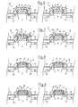
- MOS transistors 10, 11 respectively N-channel and P-channel, formed according to the known technique.
- a gate 2 is formed comprising a gate oxide layer 3 and a polysilicon layer 4.
- the gate 2 there are defined two areas 50 for the formation of first lightly doped N- diffusions 5A of source and drain for MOS transistor 10, obtained by means of implantation and successive diffusion of N type ions in a dose of approximately 10 12 atoms/cm 2 .
- a gate 2 comprising the gate oxide layer 3 and the polysilicon layer 4.
- dielectric material spacers 8 are subsequently formed, by means of conventional techniques, dielectric material spacers 8 on both sides of the gate 2.
- implantations of N type ions at high dose approximately of 10 15 atoms/cm 2 , so to form source and drain sub-regions 12 heavily doped N+.
- source and drain regions 5, 12 for the N-channel transistor 10 each one formed by a first sub-region 5 lightly doped N- and a second sub-regions 12 more heavily doped N+.
- source and drain regions 7, 13 for the P-channel transistor 11 each one composed of a first sub-region 7 lightly doped P- and a second sub-region 13 more heavily doped P+.
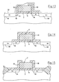
- a layer of a transition metal 14 is deposited, for example Ti and Co ( Figure 5), and a thermal process is then executed for the formation of a salicide layer 15.
- the salicide forms only where the transition metal is in contact with the silicon; over the dielectric 9 no salicide is formed; the transition metal is then removed ( Figure 6).
- Figure 6 the presence of the dielectric 9, formed to mask the lightly doped source and drain sub-regions 5 and 7 and the gate 2 of the transistors from the implantations of ions at high dose, is advantageously used to protect regions 5, 7 and the gate 2 from salicidation, thus realizing this process only in the heavily doped sub-regions 12, 13.
- the dielectric layer 9 can comprise a double layer, a first one of SiO 2 18, a second one of Si 3 N 4 19, thus avoiding the direct contact between the silicon and the nitride of said second layer 19. Also in this embodiment the overall thickness of layer 9 ranges from 200 to 500 Angstroms.
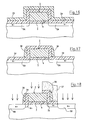
- the process according to the invention can also be applied to the salicidation of MOS transistors which, as shown in Figure 8, has a gate 2 comprising, in addition to the gate oxide layer 3 and the polysilicon layer 4, a further dielectric layer 16 suitable for example for improving the lithographic definition process of the gate, so as to avoid the contact between the polysilicon layer 4 and the overlying dielectric layer 9 used for the selective implantation of the high doses of N and P type dopants.
- the process according to the invention can be applied to the salicidation of MOS transistor in which the gate 2, as shown in Figure 9, in addition to the gate oxide layer 3 and the polysilicon layer 4, also comprises a silicide layer 17 formed over the polysilicon layer 4.
- the gate 2 since salicidation 15 cannot be performed over the silicide layer 17, the gate 2 must comprise a further dielectric layer 16 covering the silicide layer 17 where the latter is not protected by the dielectric 9.
- the gate 2 is thus defined leaving on the polysilicon 4 the layer of residual dielectric 16. Once the spacers 8 have been formed, the process according to the invention is performed.
- the insulated gate electrode of the MOSFET comprising the gate oxide 3 and the polysilicon gate 4, and after having formed lightly doped N- source and drain regions by means of a Lightly Doped Drain (LDD) implant (N- for the N-channel MOSFETs, P- for the P-channel MOSFETs, with a dopant dose of approximately 10 12 and, respectively, 10 13 atoms/cm 2 ), the structure shown in Figure 10 is obtained.
- LDD Lightly Doped Drain
- a CVD (Chemical Vapor Deposited) dielectric layer 30 is then deposited over the surface.
- the dielectric layer 30 can be for example an oxide layer formed by TEOS or a layer of nitride, and has preferably a thickness of 150 to 300 nanometers.
- a photoresist mask layer 31 is then formed over the structure.
- a selective etching of the dielectric layer 30 is then performed; where the mask layer 31 is present, the dielectric layer 30 is not removed.
- the mask layer 31 leaves a portion of the N- drain region 5A of the MOSFET covered; at the source side, instead, where the mask layer is not present, during the etching process an insulating sidewall spacer 32 is formed.
- a selective implantation of a high dose of dopants (e.g., 10 15 atoms/cm 2 ) is then performed, so as to form heavily doped N+ source and drain portions 5B. It is to be noted that this selective implant step could as well be performed using a different mask, formed over the structure after the removal of the photoresist layer 31.
- a layer of a transition metal 33 is deposited over the whole surface.
- a thermal process is then performed so as to form, where the transition metal layer is in direct contact with silicon or with polysilicon, a salicide layer, as in the first embodiment previously described.
- the dimension of the N- region 5A at the drain side can be varied as desired.
- the dielectric layer 30 is left over the whole polysilicon gate 4 of the MOSFET, and also covers a portion of the N- source region 5A.
- the salicide layer will only be formed over the heavily doped portions 5B of the source and drain regions of the MOSFET.
- the polysilicon gate 4 of the MOSFETs can comprise a layer of polycide, such as for example Wsi 2 .
- the process of Figures 10 to 13 also allows for preventing the formation of salicide over the source and drain regions of MOSFETs that do not comprise heavily doped source and drain region portions, as shown in Figure 14.
- the dielectric layer 30 can cover completely the polysilicon gate 4 or, as shown in Figure 14, the polysilicon gate 4 can be left exposed so that a salicide layer is formed over the polysilicon gate 4.
- a fourth embodiment of the invention is shown in Figures 16 to 18.
- two dielectric films 34, 35 are deposited sequentially; the two films preferably have different etch rates.
- the upper film 35 is etched.
- the etching process is stopped when the surface of the lower dielectric film 34 is reached; this can be advantageously achieved if the two films 34, 35 have different etch rates. In this way, as shown in Figure 17, dielectric sidewall spacers 36 are formed.
- a photoresist mask layer 37 is formed over a portion of the N-drain region of the MOSFET, and the lower dielectric film 34 is etched down to the silicon surface where the dielectric film 34 is not covered by either the mask layer 37 or the spacer 36.
- the mask layer 37 could also not be provided with, and in this case a symmetric structure would be obtained, with the N- portion 5A at the drain side having a same extension of the N- portion 5A at the source side.
- the upper film 35 not necessarily is a dielectric film: it could as well be a conductive, which can be selectively removed after the etching processes, before or after the implant steps.
Abstract
Description
Claims (10)
- Process for forming salicide on active areas of MOS transistors (10,11), each comprising a gate (2) and respective source and drain regions (5,12;7,13;5A,5B), the source and drain regions comprising each a first lightly doped sub-region (5;7;5A) adjacent the gate (2) and a second highly doped sub-region (12;13;5B) spaced apart from the gate (2), characterized in that the salicide is formed selectively at least over said second highly doped sub-regions (12;13;5B) of the source and drain regions of the MOS transistors, and not over said first lightly doped sub-region (5;7;5A).
- Process according to claim 1, characterized in that the salicide is formed selectively depositing a layer of a transition metal (14,33), in particular Ti or Co, at least over said second sub-regions (12;13;5B) but not over said first sub-regions (5;7;5A) of the source and drain regions of the MOS transistors, and successively making said layer of transition metal (14;33) react with the underlying silicon material by means of a thermal process.
- Process according to claim 2, characterized in that for the selective deposition of said layer of transition metal (14;33) the formation of mask means (9;30,31,32;30;34,36,37) is provided, the mask means being suitable for masking at least said first sub-regions (5;7;5A) of the source and drain regions of the MOS transistors.
- Process according to claim 3, characterized in that said mask means (9;30,31,32;30;34,36,37) comprises a same mask as that used for the selective introduction of dopants for the formation of said second sub-regions (12;13;5B) of the source and drain regions of the MOS transistors.
- Process according to claim 4, characterized in that the formation of the mask means (9;30,31,32;30;34,36,37) comprises the formation of a protective layer (9;30;34,35) and the selective removal thereof, so as to obtain a residual protective layer (9;30;34,36) at least over said first sub-regions (5;7;5A) of the source and drain regions of the MOS transistors.
- Process according to claim 5, characterized in that said residual protective layer (9;30) is also left over said gate (2).
- Process according to claim 5, characterized in that said protective layer (34;35) comprises a lower protective layer (34) and an upper protective layer (35).
- Process according to claim 7, characterized in that said lower and upper protective layers (34,35) have different etch rates.
- Process according to any one of the preceding claims, characterized in that said gate (2) is formed by a silicon oxide layer (3), a polysilicon layer (4), and a further dielectric layer (16).
- Process according to any one of claims 1 to 8, characterized in that said gate (2) is formed by a silicon oxide layer (3), a polysilicon layer (4), a silicide layer (17) and a further dielectric layer (16).
Priority Applications (1)
| Application Number | Priority Date | Filing Date | Title |
|---|---|---|---|
| EP98830235A EP0878833B1 (en) | 1997-05-13 | 1998-04-20 | Process for the selective formation of salicide on active areas of MOS devices |
Applications Claiming Priority (3)
| Application Number | Priority Date | Filing Date | Title |
|---|---|---|---|
| EP97830219 | 1997-05-13 | ||
| EP97830219 | 1997-05-13 | ||
| EP98830235A EP0878833B1 (en) | 1997-05-13 | 1998-04-20 | Process for the selective formation of salicide on active areas of MOS devices |
Publications (3)
| Publication Number | Publication Date |
|---|---|
| EP0878833A2 true EP0878833A2 (en) | 1998-11-18 |
| EP0878833A3 EP0878833A3 (en) | 1999-02-17 |
| EP0878833B1 EP0878833B1 (en) | 2010-06-23 |
Family
ID=26148137
Family Applications (1)
| Application Number | Title | Priority Date | Filing Date |
|---|---|---|---|
| EP98830235A Expired - Lifetime EP0878833B1 (en) | 1997-05-13 | 1998-04-20 | Process for the selective formation of salicide on active areas of MOS devices |
Country Status (1)
| Country | Link |
|---|---|
| EP (1) | EP0878833B1 (en) |
Citations (1)
| Publication number | Priority date | Publication date | Assignee | Title |
|---|---|---|---|---|
| US5589423A (en) | 1994-10-03 | 1996-12-31 | Motorola Inc. | Process for fabricating a non-silicided region in an integrated circuit |
Family Cites Families (6)
| Publication number | Priority date | Publication date | Assignee | Title |
|---|---|---|---|---|
| US4868138A (en) * | 1988-03-23 | 1989-09-19 | Sgs-Thomson Microelectronics, Inc. | Method for forming a self-aligned source/drain contact for an MOS transistor |
| EP0550255B1 (en) * | 1991-12-31 | 1998-03-11 | STMicroelectronics, Inc. | Transistor spacer structure |
| JPH06204173A (en) * | 1993-01-08 | 1994-07-22 | Nec Corp | Manufacture of semiconductor device |
| US5439839A (en) * | 1994-07-13 | 1995-08-08 | Winbond Electronics Corporation | Self-aligned source/drain MOS process |
| JPH0982949A (en) * | 1995-09-11 | 1997-03-28 | Denso Corp | Semiconductor device and the manufacture |
| US5605854A (en) * | 1996-02-20 | 1997-02-25 | Taiwan Semiconductor Manufacturing Company Ltd. | Integrated Ti-W polycide for deep submicron processing |
-
1998
- 1998-04-20 EP EP98830235A patent/EP0878833B1/en not_active Expired - Lifetime
Patent Citations (1)
| Publication number | Priority date | Publication date | Assignee | Title |
|---|---|---|---|---|
| US5589423A (en) | 1994-10-03 | 1996-12-31 | Motorola Inc. | Process for fabricating a non-silicided region in an integrated circuit |
Also Published As
| Publication number | Publication date |
|---|---|
| EP0878833B1 (en) | 2010-06-23 |
| EP0878833A3 (en) | 1999-02-17 |
Similar Documents
| Publication | Publication Date | Title |
|---|---|---|
| US5963803A (en) | Method of making N-channel and P-channel IGFETs with different gate thicknesses and spacer widths | |
| US6074915A (en) | Method of making embedded flash memory with salicide and sac structure | |
| US6136636A (en) | Method of manufacturing deep sub-micron CMOS transistors | |
| US5933721A (en) | Method for fabricating differential threshold voltage transistor pair | |
| US5998849A (en) | Semiconductor device having highly-doped source/drain regions with interior edges in a dislocation-free state | |
| US7544573B2 (en) | Semiconductor device including MOS field effect transistor having offset spacers or gate sidewall films on either side of gate electrode and method of manufacturing the same | |
| US20010046695A1 (en) | Method of forming silicide | |
| US6096591A (en) | Method of making an IGFET and a protected resistor with reduced processing steps | |
| WO1998048457A1 (en) | Method of making nmos and pmos devices with reduced masking steps | |
| US20020119648A1 (en) | Method for fabricating semiconductor device | |
| EP1005081A2 (en) | Semiconductor nonvolatile memory and manufacturing method thereof | |
| US5854115A (en) | Formation of an etch stop layer within a transistor gate conductor to provide for reduction of channel length | |
| US6004849A (en) | Method of making an asymmetrical IGFET with a silicide contact on the drain without a silicide contact on the source | |
| US6207482B1 (en) | Integration method for deep sub-micron dual gate transistor design | |
| US6800901B2 (en) | Process for the selective formation of salicide on active areas of MOS devices | |
| US6008100A (en) | Metal-oxide semiconductor field effect transistor device fabrication process | |
| JPH08213610A (en) | Field effect transistor and its manufacturing method | |
| KR100655069B1 (en) | Method for fabricating dual gate type MOS transistor | |
| JP3518059B2 (en) | Method of manufacturing MIS transistor | |
| US6150244A (en) | Method for fabricating MOS transistor having raised source and drain | |
| KR20050087660A (en) | Fabrication method of a mos transistor having a total silicide gate | |
| EP0878833B1 (en) | Process for the selective formation of salicide on active areas of MOS devices | |
| US5976924A (en) | Method of making a self-aligned disposable gate electrode for advanced CMOS design | |
| US7271414B2 (en) | Semiconductor device and method for fabricating the same | |
| KR20010066327A (en) | A method for fabricating dual gate electrode |
Legal Events
| Date | Code | Title | Description |
|---|---|---|---|
| PUAI | Public reference made under article 153(3) epc to a published international application that has entered the european phase |
Free format text: ORIGINAL CODE: 0009012 |
|
| AK | Designated contracting states |
Kind code of ref document: A2 Designated state(s): AT BE CH CY DE DK ES FI FR GB GR IE IT LI LU MC NL PT SE |
|
| AX | Request for extension of the european patent |
Free format text: AL;LT;LV;MK;RO;SI |
|
| PUAL | Search report despatched |
Free format text: ORIGINAL CODE: 0009013 |
|
| AK | Designated contracting states |
Kind code of ref document: A3 Designated state(s): AT BE CH CY DE DK ES FI FR GB GR IE IT LI LU MC NL PT SE |
|
| AX | Request for extension of the european patent |
Free format text: AL;LT;LV;MK;RO;SI |
|
| AKX | Designation fees paid | ||
| REG | Reference to a national code |
Ref country code: DE Ref legal event code: 8566 |
|
| 17P | Request for examination filed |
Effective date: 19990629 |
|
| RBV | Designated contracting states (corrected) |
Designated state(s): DE FR GB IT |
|
| 17Q | First examination report despatched |
Effective date: 20090217 |
|
| GRAP | Despatch of communication of intention to grant a patent |
Free format text: ORIGINAL CODE: EPIDOSNIGR1 |
|
| GRAS | Grant fee paid |
Free format text: ORIGINAL CODE: EPIDOSNIGR3 |
|
| RAP1 | Party data changed (applicant data changed or rights of an application transferred) |
Owner name: STMICROELECTRONICS SRL |
|
| GRAA | (expected) grant |
Free format text: ORIGINAL CODE: 0009210 |
|
| AK | Designated contracting states |
Kind code of ref document: B1 Designated state(s): DE FR GB IT |
|
| REF | Corresponds to: |
Ref document number: 69841732 Country of ref document: DE Date of ref document: 20100805 Kind code of ref document: P |
|
| PLBE | No opposition filed within time limit |
Free format text: ORIGINAL CODE: 0009261 |
|
| STAA | Information on the status of an ep patent application or granted ep patent |
Free format text: STATUS: NO OPPOSITION FILED WITHIN TIME LIMIT |
|
| 26N | No opposition filed |
Effective date: 20110324 |
|
| REG | Reference to a national code |
Ref country code: DE Ref legal event code: R097 Ref document number: 69841732 Country of ref document: DE Effective date: 20110323 |
|
| REG | Reference to a national code |
Ref country code: FR Ref legal event code: PLFP Year of fee payment: 19 |
|
| REG | Reference to a national code |
Ref country code: FR Ref legal event code: PLFP Year of fee payment: 20 |
|
| PGFP | Annual fee paid to national office [announced via postgrant information from national office to epo] |
Ref country code: FR Payment date: 20170322 Year of fee payment: 20 |
|
| PGFP | Annual fee paid to national office [announced via postgrant information from national office to epo] |
Ref country code: GB Payment date: 20170324 Year of fee payment: 20 |
|
| PGFP | Annual fee paid to national office [announced via postgrant information from national office to epo] |
Ref country code: IT Payment date: 20170322 Year of fee payment: 20 |
|
| PGFP | Annual fee paid to national office [announced via postgrant information from national office to epo] |
Ref country code: DE Payment date: 20170321 Year of fee payment: 20 |
|
| REG | Reference to a national code |
Ref country code: DE Ref legal event code: R071 Ref document number: 69841732 Country of ref document: DE |
|
| REG | Reference to a national code |
Ref country code: GB Ref legal event code: PE20 Expiry date: 20180419 |
|
| PG25 | Lapsed in a contracting state [announced via postgrant information from national office to epo] |
Ref country code: GB Free format text: LAPSE BECAUSE OF EXPIRATION OF PROTECTION Effective date: 20180419 |