EP0877272B1 - Improvements in or relating to spatial light modulators - Google Patents
Improvements in or relating to spatial light modulators Download PDFInfo
- Publication number
- EP0877272B1 EP0877272B1 EP98201538A EP98201538A EP0877272B1 EP 0877272 B1 EP0877272 B1 EP 0877272B1 EP 98201538 A EP98201538 A EP 98201538A EP 98201538 A EP98201538 A EP 98201538A EP 0877272 B1 EP0877272 B1 EP 0877272B1
- Authority
- EP
- European Patent Office
- Prior art keywords
- edges
- light
- support
- yoke
- specified
- Prior art date
- Legal status (The legal status is an assumption and is not a legal conclusion. Google has not performed a legal analysis and makes no representation as to the accuracy of the status listed.)
- Expired - Lifetime
Links
- 238000000034 method Methods 0.000 description 4
- 230000003287 optical effect Effects 0.000 description 3
- 239000006096 absorbing agent Substances 0.000 description 2
- 239000000463 material Substances 0.000 description 2
- 238000012986 modification Methods 0.000 description 2
- 230000004048 modification Effects 0.000 description 2
- 239000000758 substrate Substances 0.000 description 2
- 101100277916 Caenorhabditis elegans dmd-10 gene Proteins 0.000 description 1
- OAICVXFJPJFONN-UHFFFAOYSA-N Phosphorus Chemical compound [P] OAICVXFJPJFONN-UHFFFAOYSA-N 0.000 description 1
- 230000000694 effects Effects 0.000 description 1
- 230000001747 exhibiting effect Effects 0.000 description 1
- 230000010365 information processing Effects 0.000 description 1
- 239000004973 liquid crystal related substance Substances 0.000 description 1
- 238000004519 manufacturing process Methods 0.000 description 1
- 230000010287 polarization Effects 0.000 description 1
Images


Classifications
-
- G—PHYSICS
- G02—OPTICS
- G02B—OPTICAL ELEMENTS, SYSTEMS OR APPARATUS
- G02B26/00—Optical devices or arrangements for the control of light using movable or deformable optical elements
- G02B26/08—Optical devices or arrangements for the control of light using movable or deformable optical elements for controlling the direction of light
- G02B26/0816—Optical devices or arrangements for the control of light using movable or deformable optical elements for controlling the direction of light by means of one or more reflecting elements
- G02B26/0833—Optical devices or arrangements for the control of light using movable or deformable optical elements for controlling the direction of light by means of one or more reflecting elements the reflecting element being a micromechanical device, e.g. a MEMS mirror, DMD
- G02B26/0841—Optical devices or arrangements for the control of light using movable or deformable optical elements for controlling the direction of light by means of one or more reflecting elements the reflecting element being a micromechanical device, e.g. a MEMS mirror, DMD the reflecting element being moved or deformed by electrostatic means
Definitions
- the present invention is generally related to spatial light modulators for modulating incident light to form a video image, and more particularity, to a digital micromirror device (DMD) having an array of bistable micromirrors fabricated over addressing circuitry .
- DMD digital micromirror device
- SLMs Spatial Light Modulators
- SLMs have found numerous applications in the areas of optical information processing, projection displays, video and graphics monitors, televisions, and electrophotographic printing.
- SLMs are devices that modulate incident light in a spatial pattern to form a light image corresponding to an electrical or optical input.
- the incident light may be modulated in its phase, intensity, polarization, or direction.
- the light modulation may be achieved by a variety of materials exhibiting various electro-optic or magneto-optic effects, and by materials that modulate light by surface deformation.
- An SLM is typically comprised of an area or linear array of addressable picture elements (pixels).
- Source pixel data is first formatted by an associated control circuit, usually external to the SLM, and then loaded into the pixel array one frame at a time.
- This pixel data may be written to the pixel array using a variety of algorithms, i.e. sequentially top-to-bottom one pixel line at a time, interleaving by sequentially addressing top-to-bottom ever other pixel line, such as the odd rows of pixels, and then returning to address the even pixel lines, etc.
- this data writing technique is know as rasterizing, whereby a high powered electron gun scans across the pixel elements of a phosphor screen left to right, one line at a time.
- This pixel address data writing scheme is equally applicable to liquid crystal displays (LCDs) as well.
- DMD digital micromirror device or the deformable mirror device
- the DMD is revolutionary in that it is truly a digital display device and an integrated circuit solution.
- the DMD is an electro/mechanical/optical SLM suitable for use in displays, projectors and hardcopy printers.
- the DMD is a monolithic single-chip integrated circuit SLM, comprised of a high density array of 16 micron square movable micromirrors on 17 micron centers. These mirrors are fabricated over address circuitry including an array of SRAM cells and address electrodes.
- Each mirror forms one pixel of the DMD array and is bistable, that is to say, stable in one of two positions, wherein a source of light directed upon the mirror array will be reflected in one of two directions.
- incident light to that mirror will be reflected to a projector lens and focused on a display screen or a photosensitive element of a printer.
- the other "OFF" mirror position light directed on the mirror will be deflected to a light absorber.
- Each mirror of the array is individually controlled to either direct incident light into the projector lens, or to the light absorber.
- the projector lens ultimately focuses and magnifies the modulated light from the pixel mirrors onto a display screen and produce an image in the case of a display. If each pixel mirror of the DMD array is in the "ON" position, the displayed image will be an array of bright pixels.
- DMD 10 digital micromirror device
- DMD 10 is a single-chip integrated. circuit seen to include an array of micromirrors 30 monolithically fabricated over a memory cell array formed upon the substrate. Each pixel mirror 30 is seen to include a square mirror supported upon and elevated above a butterfly shaped yoke generally shown at 32 by a rectangular support post 34.
- Support post 34 extends downward from the center of the mirror 30, and is attached to the center of the yoke 32 along a torsion axis thereof, as shown, to balance the center of mass of mirror 30 upon yoke 32.
- Yoke 32 is axially supported along a central axis thereof by a pair of torsion hinges 40.
- the other end of each torsion hinge 40 is attached to and supported by a hinge support post cap 42 defined on top of a respective hinge support post 44.
- a pair of elevated mirror address electrodes 50 and 54 are supported by a respective address support post.
- the address support posts, and the hinge support posts 44 support the address electrodes 50 and 54, the torsion hinges 40, and the yoke 32 away from and above a bias/reset bus 60, and a pair of substrate level address electrode pads 26 and 28.
- mirror 30 and yoke 32 are together rotated about the torsion axis of the yoke, defined by the hinges 40, a pair of yoke tips 58 on the side of the yoke 32 that is deflected land upon and engage the bias/reset bus 60 at a landing site 62.
- this conventional DMD see the teachings of commonly assigned U.S. Patent 5,535,047.
- the support post 34 extends downward from the reflective modulation surface of the square mirror 30 and defines support post edges at 64.
- These support post edges 64 conventionally have dimensions of 3 X 4 um, which edges form a rectangle and are oriented either perpendicular or parallel to the incoming beam of light.
- FIG 2 there is shown the light diffracted back into the projection optics when all mirrors are in the off-state. It can be seen that these support post edges 64 defract the incident light into the projection system optics when the mirrors 30 are tilted to the off state, the diffraction seen as light dots 66, thus reducing the contrast ratio of the formed display image. Also seen in Figure 2 is defracted light from the underlying superstructure and address circuitry from between the mirror edges.
- DMD spatial light modulator forming an image having an improved contrast ratio whereby the defraction of incident light from the support post edges 64 into the projection optics is substantially reduced.
- the present invention as defined by claims 1 and 7 achieves technical advantages as a micromechanical spatial light modulator by orienting the support post edges to be parallel to the mirror edges, and orienting the mirror edges at 45 degrees with respect to incident light.
- the dimensions of the support post edges are substantially reduced from 3 X 4 ⁇ m to 2.4 X 2.4 ⁇ m. This design substantially reduces the amount of scattered light from the support post edges back into the darkfield projection system optics.
- the corners formed by support post edges defract a minimal amount of light back into the projection optics in this orientation.
- the support post edges are parallel with the corresponding mirror edges, and are also oriented at 45 degrees with respect to the incident light to minimize light defraction therefrom.
- Spatial light modulator 70 is preferably a digital micromirror device (DMD), however, other micromechanical spatial light modulators are intended to be covered by the present invention as well.
- DMD digital micromirror device
- DMD 70 is improved over the conventional design shown in Figure 1 by providing each mirror 72 with a mirror support post 74 defining support post edges 76 that are all oriented at 45 degrees with respect to the incident beam of light generated by light source 80.
- Each edge 76 is parallel to the corresponding mirror edges 78 of the respective mirrors 72, and thus edges 78 are also oriented at 45 degrees with respect to the incident beam of light generated by light source 80.
- This orientation of support post edges 76 with respect to the incident light beam minimizes any defraction of light from being scattered back into the darkfield projection system optics when the mirror surfaces are oriented in the off-state. This is important to increase the contrast ratio of the display formed by SLM 70.
- the dimensions of the support post edges 76 have been substantially reduced from that of conventional designs. Specifically, the edges 76 have been reduced to a length of about 2.4 X 2.4 ⁇ m, which is substantially reduced from conventional dimensions shown in Figure 1 which are typically 3 X 4 ⁇ m. Minimizing the length of the support post edges 76 also contributes to an improved contrast ratio of the image displayed by the spatial light modulator 70 according to the preferred embodiment of the present invention.
Landscapes
- Physics & Mathematics (AREA)
- General Physics & Mathematics (AREA)
- Optics & Photonics (AREA)
- Mechanical Light Control Or Optical Switches (AREA)
- Transforming Electric Information Into Light Information (AREA)
- Devices For Indicating Variable Information By Combining Individual Elements (AREA)
Description
- The present invention is generally related to spatial light modulators for modulating incident light to form a video image, and more particularity, to a digital micromirror device (DMD) having an array of bistable micromirrors fabricated over addressing circuitry .
- Spatial Light Modulators (SLMs) have found numerous applications in the areas of optical information processing, projection displays, video and graphics monitors, televisions, and electrophotographic printing. SLMs are devices that modulate incident light in a spatial pattern to form a light image corresponding to an electrical or optical input. The incident light may be modulated in its phase, intensity, polarization, or direction. The light modulation may be achieved by a variety of materials exhibiting various electro-optic or magneto-optic effects, and by materials that modulate light by surface deformation.
- An SLM is typically comprised of an area or linear array of addressable picture elements (pixels). Source pixel data is first formatted by an associated control circuit, usually external to the SLM, and then loaded into the pixel array one frame at a time. This pixel data may be written to the pixel array using a variety of algorithms, i.e. sequentially top-to-bottom one pixel line at a time, interleaving by sequentially addressing top-to-bottom ever other pixel line, such as the odd rows of pixels, and then returning to address the even pixel lines, etc. In cathode ray tubes (CRTs), this data writing technique is know as rasterizing, whereby a high powered electron gun scans across the pixel elements of a phosphor screen left to right, one line at a time. This pixel address data writing scheme is equally applicable to liquid crystal displays (LCDs) as well.
- A recent innovation of Texas Instruments Incorporated of Dallas, Texas, is the digital micromirror device or the deformable mirror device (collectively DMD). The DMD is revolutionary in that it is truly a digital display device and an integrated circuit solution. The DMD is an electro/mechanical/optical SLM suitable for use in displays, projectors and hardcopy printers. The DMD is a monolithic single-chip integrated circuit SLM, comprised of a high density array of 16 micron square movable micromirrors on 17 micron centers. These mirrors are fabricated over address circuitry including an array of SRAM cells and address electrodes. Each mirror forms one pixel of the DMD array and is bistable, that is to say, stable in one of two positions, wherein a source of light directed upon the mirror array will be reflected in one of two directions. In one stable "ON" mirror position, incident light to that mirror will be reflected to a projector lens and focused on a display screen or a photosensitive element of a printer. In the other "OFF" mirror position, light directed on the mirror will be deflected to a light absorber. Each mirror of the array is individually controlled to either direct incident light into the projector lens, or to the light absorber. The projector lens ultimately focuses and magnifies the modulated light from the pixel mirrors onto a display screen and produce an image in the case of a display. If each pixel mirror of the DMD array is in the "ON" position, the displayed image will be an array of bright pixels.
- For a more detailed discussion of the DMD device and uses, cross reference is made to U.S. Patent 5,061,049 to Hornbeck, entitled "Spatial Light Modulator and Method"; U.S. Patent 5,079,544 to DeMond, et al, entitled "Standard Independent Digitized Video System"; and U.S. Patent 5,105,369 to Nelson, entitled "Printing System Exposure Module Alignment Method and Apparatus of Manufacture", each patent being assigned to the same assignee of the present invention. Gray scale of the pixels forming the image is achieved by pulse-width modulation techniques of the mirrors, such as that described in U.S. Patent 5,278,652, entitled "DMD Architecture and Timing for Use in a Pulse-Width Modulated Display System", assigned to the same assignee of the present invention.
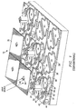
- As detailed in commonly assigned U.S. Patent 5,535,047 entitled "Active Yoke Hidden Hinge Digital Micromirror Device", and shown in Figure 1 of the present application, there is disclosed a digital micromirror device (DMD) spatial light modulator shown at 10. DMD 10 is a single-chip integrated. circuit seen to include an array of
micromirrors 30 monolithically fabricated over a memory cell array formed upon the substrate. Eachpixel mirror 30 is seen to include a square mirror supported upon and elevated above a butterfly shaped yoke generally shown at 32 by arectangular support post 34.Support post 34 extends downward from the center of themirror 30, and is attached to the center of theyoke 32 along a torsion axis thereof, as shown, to balance the center of mass ofmirror 30 uponyoke 32. Yoke 32 is axially supported along a central axis thereof by a pair oftorsion hinges 40. The other end of eachtorsion hinge 40 is attached to and supported by a hingesupport post cap 42 defined on top of a respectivehinge support post 44. A pair of elevatedmirror address electrodes hinge support posts 44, support theaddress electrodes yoke 32 away from and above a bias/reset bus 60, and a pair of substrate leveladdress electrode pads mirror 30 andyoke 32 are together rotated about the torsion axis of the yoke, defined by thehinges 40, a pair ofyoke tips 58 on the side of theyoke 32 that is deflected land upon and engage the bias/reset bus 60 at alanding site 62. For more detailed discussion of this conventional DMD, see the teachings of commonly assigned U.S. Patent 5,535,047. - Still referring to Figure 1, it can be seen that the
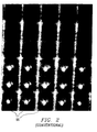
support post 34 extends downward from the reflective modulation surface of thesquare mirror 30 and defines support post edges at 64. Thesesupport post edges 64 conventionally have dimensions of 3 X 4 um, which edges form a rectangle and are oriented either perpendicular or parallel to the incoming beam of light. Referring to Figure 2, there is shown the light diffracted back into the projection optics when all mirrors are in the off-state. It can be seen that thesesupport post edges 64 defract the incident light into the projection system optics when themirrors 30 are tilted to the off state, the diffraction seen aslight dots 66, thus reducing the contrast ratio of the formed display image. Also seen in Figure 2 is defracted light from the underlying superstructure and address circuitry from between the mirror edges. - There is desired a DMD spatial light modulator forming an image having an improved contrast ratio whereby the defraction of incident light from the
support post edges 64 into the projection optics is substantially reduced. - The present invention as defined by claims 1 and 7 achieves technical advantages as a micromechanical spatial light modulator by orienting the support post edges to be parallel to the mirror edges, and orienting the mirror edges at 45 degrees with respect to incident light. In addition, the dimensions of the support post edges are substantially reduced from 3 X 4 µm to 2.4 X 2.4 µm. This design substantially reduces the amount of scattered light from the support post edges back into the darkfield projection system optics. The corners formed by support post edges defract a minimal amount of light back into the projection optics in this orientation. The support post edges are parallel with the corresponding mirror edges, and are also oriented at 45 degrees with respect to the incident light to minimize light defraction therefrom.
- The present invention will now be further described, by way of example, with reference to the accompanying drawings in which:
- Figure 1 is a section view of a 3 X 3 array of pixels of a conventional DMD array with the yokes elevated address electrodes, and some hinge support posts being removed to illustrate underlying support structure, whereby the mirror support post edges are either perpendicular and parallel to the incident light and thus defract incident light back into the projection optics, the dimensions of these support post edges being approximately 3 X 4 µm;
- Figure 2 is a pictorial view of an image formed by the array of mirrors of Figure 1 in the off-state, whereby light is defracted from the support post edges back into the projection optics, shown as light dots, thereby reducing the contrast ratio of the image formed by the spatial light modulator;
- Figure 3 is a section view of a 3 X 3 array of pixels according to the present invention whereby the support post edges are all oriented at 45 degrees with respect to the incident light, each edge being parallel to the corresponding mirror edges, to substantially reduce the amount of defracted light back into the projection optics when oriented in the off-state; and
- Figure 4 is a pictorial view of the defracted light from the support post edges of Figure 3 in the off-state, illustrating a minimal amount of light being defracted from the support post edges back into the projection optics, thereby significantly increasing the contrast ratio of the display image.
-
- Referring now to Figure 3, there is shown at 70 an improved spatial light modulator according to the preferred embodiment of the present invention, wherein like numerals refer to like elements.
Spatial light modulator 70 is preferably a digital micromirror device (DMD), however, other micromechanical spatial light modulators are intended to be covered by the present invention as well. - DMD 70 is improved over the conventional design shown in Figure 1 by providing each
mirror 72 with amirror support post 74 definingsupport post edges 76 that are all oriented at 45 degrees with respect to the incident beam of light generated bylight source 80. Eachedge 76 is parallel to thecorresponding mirror edges 78 of therespective mirrors 72, and thusedges 78 are also oriented at 45 degrees with respect to the incident beam of light generated bylight source 80. This orientation ofsupport post edges 76 with respect to the incident light beam minimizes any defraction of light from being scattered back into the darkfield projection system optics when the mirror surfaces are oriented in the off-state. This is important to increase the contrast ratio of the display formed bySLM 70. For darkfield optics systems, it is imperative that as little light as possible be defracted back into the optics when themirrors 72 are in the off-state. By orienting thesupport post edges 76 to extend at 45 degrees with respect to the incident beam of light, this defraction of light is minimized, and the generation oflight dots 66 diffracted by the mirrors in the off-state into the projection optics, as seen in Figure 2, are substantially reduced. Any defraction of light from the corners defined by theedges 76 into the projection optics is also substantially reduced. - According to the present invention, the dimensions of the
support post edges 76 have been substantially reduced from that of conventional designs. Specifically, theedges 76 have been reduced to a length of about 2.4 X 2.4 µm, which is substantially reduced from conventional dimensions shown in Figure 1 which are typically 3 X 4 µm. Minimizing the length of the support post edges 76 also contributes to an improved contrast ratio of the image displayed by the spatiallight modulator 70 according to the preferred embodiment of the present invention. - In previous designs, it was believed that orienting the support post edges 62, as shown in Figure 1, to either be parallel to or perpendicular to the incoming beam of light was necessary to minimize defraction of light from the support post corners. However, by reducing the dimensions of the support post edges 76, and orienting these
edges 76 to extend at 45 degrees with respect to the incident beam of light has proven to provide an image with a substantially improved contrast ratio, as shown in Figure 4. The amount of scattered light from the support post edges 76, and from the corners defined by these edges, is substantially reduced as compared to the conventional display shown for comparison in Figure 4. In fact, an improved contrast ratio of about 20% is achieved over the embodiment of Figure 1. Thus, the improvement of the present invention has dramatic results. - Though the invention has been described with respect to a specific preferred embodiment, many variations and modifications will become apparent to those skilled in the art upon reading the present application. It is therefore the intention that the appended claims be interpreted as broadly as possible in view of the prior art to include all such variations and modifications.
Claims (11)
- A spatial light modulator, comprising:a support structure including a deflectable yoke;means for deflecting said yoke; anda pixel elevated above and supported by said yoke, said pixel having a light modulation surface defining surface edges anda support member extending between said surface and said yoke, said support member defining support edges in said surface, that are substantially parallel to surface edges.
- The spatial light modulator as specified in Claim 1, wherein said surface edges and said support edges both define a rectangle.
- The spatial light modulator as specified in Claim 1 or Claim 2, wherein said support member is centrally located with respect to said light modulation surface.
- The spatial light modulator as specified in any of Claims 1 to 3, wherein said support member extends perpendicular from said light modulation surface.
- The spatial light modulator as specified in any of Claims 1 to 4, further comprising:a light source for generating a light beam incident to said light modulation surface defining an angle of incidence, said surface edges and said support edges both extending substantially at 45 degrees with respect to said angle of incidence.
- The spatial light modulator as specified in any of Claims 1 to 5, wherein said support edges define an area no greater than 5.76 µm2.
- A display system, comprising:a light source for generating a light beam;a support structure including a yoke;means for deflecting said yoke; anda pixel elevated above and supported by said yoke, said. pixel having a light modulation surface defining surface edges and having a support member extending between said surface and said yoke, said support member defining support edges in said surface, said support edges being substantially parallel to surface edges, wherein said light beam is incident to said light modulation surface and generates an angle of incidence with respect thereto, said angle of incidence being substantially 45 degrees with respect to both said support edges and said surface edges.
- The display system as specified in Claim 7, wherein said surface edges and said support edges both define a rectangle.
- The display system as specified in Claim 7 or Claim 8, wherein said support member is centrally located with respect to said light modulation surface.
- The display system as specified in any of Claims 7 to 9, wherein said support member extends substantially perpendicular from said light modulation surface.
- The display system as specified in any of Claims 7 to 10, wherein said support edges define an area no greater than 5.76 µm2.
Applications Claiming Priority (2)
| Application Number | Priority Date | Filing Date | Title |
|---|---|---|---|
| US4598697P | 1997-05-08 | 1997-05-08 | |
| US45986P | 1997-05-08 |
Publications (2)
| Publication Number | Publication Date |
|---|---|
| EP0877272A1 EP0877272A1 (en) | 1998-11-11 |
| EP0877272B1 true EP0877272B1 (en) | 2002-07-31 |
Family
ID=21940942
Family Applications (1)
| Application Number | Title | Priority Date | Filing Date |
|---|---|---|---|
| EP98201538A Expired - Lifetime EP0877272B1 (en) | 1997-05-08 | 1998-05-04 | Improvements in or relating to spatial light modulators |
Country Status (4)
| Country | Link |
|---|---|
| US (2) | US5943157A (en) |
| EP (1) | EP0877272B1 (en) |
| JP (1) | JP4406098B2 (en) |
| DE (1) | DE69806846T2 (en) |
Families Citing this family (257)
| Publication number | Priority date | Publication date | Assignee | Title |
|---|---|---|---|---|
| US6674562B1 (en) | 1994-05-05 | 2004-01-06 | Iridigm Display Corporation | Interferometric modulation of radiation |
| US6680792B2 (en) * | 1994-05-05 | 2004-01-20 | Iridigm Display Corporation | Interferometric modulation of radiation |
| US7123216B1 (en) * | 1994-05-05 | 2006-10-17 | Idc, Llc | Photonic MEMS and structures |
| US7460291B2 (en) | 1994-05-05 | 2008-12-02 | Idc, Llc | Separable modulator |
| US7297471B1 (en) | 2003-04-15 | 2007-11-20 | Idc, Llc | Method for manufacturing an array of interferometric modulators |
| US7550794B2 (en) * | 2002-09-20 | 2009-06-23 | Idc, Llc | Micromechanical systems device comprising a displaceable electrode and a charge-trapping layer |
| US7138984B1 (en) | 2001-06-05 | 2006-11-21 | Idc, Llc | Directly laminated touch sensitive screen |
| US8014059B2 (en) * | 1994-05-05 | 2011-09-06 | Qualcomm Mems Technologies, Inc. | System and method for charge control in a MEMS device |
| US6969635B2 (en) | 2000-12-07 | 2005-11-29 | Reflectivity, Inc. | Methods for depositing, releasing and packaging micro-electromechanical devices on wafer substrates |
| US7907319B2 (en) | 1995-11-06 | 2011-03-15 | Qualcomm Mems Technologies, Inc. | Method and device for modulating light with optical compensation |
| US7471444B2 (en) * | 1996-12-19 | 2008-12-30 | Idc, Llc | Interferometric modulation of radiation |
| DE69806846T2 (en) * | 1997-05-08 | 2002-12-12 | Texas Instruments Inc., Dallas | Improvements for spatial light modulators |
| US6028690A (en) * | 1997-11-26 | 2000-02-22 | Texas Instruments Incorporated | Reduced micromirror mirror gaps for improved contrast ratio |
| US8928967B2 (en) | 1998-04-08 | 2015-01-06 | Qualcomm Mems Technologies, Inc. | Method and device for modulating light |
| US7532377B2 (en) | 1998-04-08 | 2009-05-12 | Idc, Llc | Movable micro-electromechanical device |
| WO1999052006A2 (en) | 1998-04-08 | 1999-10-14 | Etalon, Inc. | Interferometric modulation of radiation |
| US6523961B2 (en) | 2000-08-30 | 2003-02-25 | Reflectivity, Inc. | Projection system and mirror elements for improved contrast ratio in spatial light modulators |
| US6344641B1 (en) * | 1999-08-11 | 2002-02-05 | Agilent Technologies, Inc. | System and method for on-chip calibration of illumination sources for an integrated circuit display |
| WO2003007049A1 (en) * | 1999-10-05 | 2003-01-23 | Iridigm Display Corporation | Photonic mems and structures |
| US6396619B1 (en) | 2000-01-28 | 2002-05-28 | Reflectivity, Inc. | Deflectable spatial light modulator having stopping mechanisms |
| US6741383B2 (en) | 2000-08-11 | 2004-05-25 | Reflectivity, Inc. | Deflectable micromirrors with stopping mechanisms |
| US6583916B2 (en) | 1999-11-03 | 2003-06-24 | Optodot Corporation | Optical shutter assembly |
| US6724512B2 (en) | 1999-11-03 | 2004-04-20 | Optodot Corporation | Optical switch device |
| US20020071169A1 (en) | 2000-02-01 | 2002-06-13 | Bowers John Edward | Micro-electro-mechanical-system (MEMS) mirror device |
| US6585383B2 (en) | 2000-05-18 | 2003-07-01 | Calient Networks, Inc. | Micromachined apparatus for improved reflection of light |
| US6560384B1 (en) | 2000-06-01 | 2003-05-06 | Calient Networks, Inc. | Optical switch having mirrors arranged to accommodate freedom of movement |
| CN100371763C (en) * | 2000-08-03 | 2008-02-27 | 反射公司 | Projection display and encapsulation micro-lens array for projection display |
| US6943950B2 (en) * | 2000-08-07 | 2005-09-13 | Texas Instruments Incorporated | Two-dimensional blazed MEMS grating |
| US6643425B1 (en) | 2000-08-17 | 2003-11-04 | Calient Networks, Inc. | Optical switch having switch mirror arrays controlled by scanning beams |
| US7300162B2 (en) | 2000-08-30 | 2007-11-27 | Texas Instruments Incorporated | Projection display |
| US6825967B1 (en) | 2000-09-29 | 2004-11-30 | Calient Networks, Inc. | Shaped electrodes for micro-electro-mechanical-system (MEMS) devices to improve actuator performance and methods for fabricating the same |
| US6962771B1 (en) * | 2000-10-13 | 2005-11-08 | Taiwan Semiconductor Manufacturing Company, Ltd. | Dual damascene process |
| US6614576B2 (en) * | 2000-12-15 | 2003-09-02 | Texas Instruments Incorporated | Surface micro-planarization for enhanced optical efficiency and pixel performance in SLM devices |
| JP4560958B2 (en) * | 2000-12-21 | 2010-10-13 | 日本テキサス・インスツルメンツ株式会社 | Micro electro mechanical system |
| US6792177B2 (en) | 2001-03-12 | 2004-09-14 | Calient Networks, Inc. | Optical switch with internal monitoring |
| DE60230942D1 (en) * | 2001-03-19 | 2009-03-12 | Texas Instruments Inc | Control clock for spatial light modulator |
| US6589625B1 (en) | 2001-08-01 | 2003-07-08 | Iridigm Display Corporation | Hermetic seal and method to create the same |
| US7023606B2 (en) | 2001-08-03 | 2006-04-04 | Reflectivity, Inc | Micromirror array for projection TV |
| US6544863B1 (en) | 2001-08-21 | 2003-04-08 | Calient Networks, Inc. | Method of fabricating semiconductor wafers having multiple height subsurface layers |
| DE60214111T2 (en) * | 2001-11-21 | 2007-02-22 | Texas Instruments Inc., Dallas | Jocheless digital micromirror device with concealed joint |
| US6856446B2 (en) * | 2001-12-12 | 2005-02-15 | Texas Instruments Incorporated | Digital micromirror device having mirror-attached spring tips |
| US7158180B2 (en) * | 2001-12-31 | 2007-01-02 | Texas Instruments Incorporated | System and method for varying exposure time for different parts of a field of view while acquiring an image |
| US6794119B2 (en) * | 2002-02-12 | 2004-09-21 | Iridigm Display Corporation | Method for fabricating a structure for a microelectromechanical systems (MEMS) device |
| US6574033B1 (en) | 2002-02-27 | 2003-06-03 | Iridigm Display Corporation | Microelectromechanical systems device and method for fabricating same |
| US6992810B2 (en) * | 2002-06-19 | 2006-01-31 | Miradia Inc. | High fill ratio reflective spatial light modulator with hidden hinge |
| US20040004753A1 (en) * | 2002-06-19 | 2004-01-08 | Pan Shaoher X. | Architecture of a reflective spatial light modulator |
| US20030234994A1 (en) * | 2002-06-19 | 2003-12-25 | Pan Shaoher X. | Reflective spatial light modulator |
| US7206110B2 (en) * | 2002-06-19 | 2007-04-17 | Miradia Inc. | Memory cell dual protection |
| US20040069742A1 (en) * | 2002-06-19 | 2004-04-15 | Pan Shaoher X. | Fabrication of a reflective spatial light modulator |
| US7034984B2 (en) | 2002-06-19 | 2006-04-25 | Miradia Inc. | Fabrication of a high fill ratio reflective spatial light modulator with hidden hinge |
| US7781850B2 (en) * | 2002-09-20 | 2010-08-24 | Qualcomm Mems Technologies, Inc. | Controlling electromechanical behavior of structures within a microelectromechanical systems device |
| TW200413810A (en) | 2003-01-29 | 2004-08-01 | Prime View Int Co Ltd | Light interference display panel and its manufacturing method |
| US7042622B2 (en) | 2003-10-30 | 2006-05-09 | Reflectivity, Inc | Micromirror and post arrangements on substrates |
| US7085035B2 (en) * | 2003-02-12 | 2006-08-01 | Reflectivity, Inc | Display apparatus with improved contrast ratio |
| US7489024B2 (en) * | 2003-02-20 | 2009-02-10 | Technion Research & Development Foundation Ltd. | TMOS-infrared uncooled sensor and focal plane array |
| US7375874B1 (en) | 2003-03-22 | 2008-05-20 | Active Optical Mems Inc. | Light modulator with integrated drive and control circuitry |
| US7015885B2 (en) | 2003-03-22 | 2006-03-21 | Active Optical Networks, Inc. | MEMS devices monolithically integrated with drive and control circuitry |
| US6914711B2 (en) * | 2003-03-22 | 2005-07-05 | Active Optical Networks, Inc. | Spatial light modulator with hidden comb actuator |
| TW594360B (en) * | 2003-04-21 | 2004-06-21 | Prime View Int Corp Ltd | A method for fabricating an interference display cell |
| TW570896B (en) | 2003-05-26 | 2004-01-11 | Prime View Int Co Ltd | A method for fabricating an interference display cell |
| US7221495B2 (en) * | 2003-06-24 | 2007-05-22 | Idc Llc | Thin film precursor stack for MEMS manufacturing |
| TW200506479A (en) * | 2003-08-15 | 2005-02-16 | Prime View Int Co Ltd | Color changeable pixel for an interference display |
| TWI231865B (en) * | 2003-08-26 | 2005-05-01 | Prime View Int Co Ltd | An interference display cell and fabrication method thereof |
| TWI232333B (en) * | 2003-09-03 | 2005-05-11 | Prime View Int Co Ltd | Display unit using interferometric modulation and manufacturing method thereof |
| TW593126B (en) * | 2003-09-30 | 2004-06-21 | Prime View Int Co Ltd | A structure of a micro electro mechanical system and manufacturing the same |
| US6914709B2 (en) * | 2003-10-02 | 2005-07-05 | Hewlett-Packard Development Company, L.P. | MEMS device and method of forming MEMS device |
| US6861277B1 (en) | 2003-10-02 | 2005-03-01 | Hewlett-Packard Development Company, L.P. | Method of forming MEMS device |
| US7183618B2 (en) * | 2004-08-14 | 2007-02-27 | Fusao Ishii | Hinge for micro-mirror devices |
| US7012726B1 (en) | 2003-11-03 | 2006-03-14 | Idc, Llc | MEMS devices with unreleased thin film components |
| US7026695B2 (en) * | 2003-11-19 | 2006-04-11 | Miradia Inc. | Method and apparatus to reduce parasitic forces in electro-mechanical systems |
| US7142346B2 (en) | 2003-12-09 | 2006-11-28 | Idc, Llc | System and method for addressing a MEMS display |
| US7161728B2 (en) | 2003-12-09 | 2007-01-09 | Idc, Llc | Area array modulation and lead reduction in interferometric modulators |
| DE10358967B4 (en) | 2003-12-15 | 2006-11-16 | Universität Kassel | Micromirror array |
| US20050162727A1 (en) * | 2004-01-24 | 2005-07-28 | Fusao Ishii | Micromirrors with support walls |
| US7532194B2 (en) * | 2004-02-03 | 2009-05-12 | Idc, Llc | Driver voltage adjuster |
| US7119945B2 (en) | 2004-03-03 | 2006-10-10 | Idc, Llc | Altering temporal response of microelectromechanical elements |
| US7706050B2 (en) * | 2004-03-05 | 2010-04-27 | Qualcomm Mems Technologies, Inc. | Integrated modulator illumination |
| US7855824B2 (en) * | 2004-03-06 | 2010-12-21 | Qualcomm Mems Technologies, Inc. | Method and system for color optimization in a display |
| US7060895B2 (en) * | 2004-05-04 | 2006-06-13 | Idc, Llc | Modifying the electro-mechanical behavior of devices |
| US7476327B2 (en) * | 2004-05-04 | 2009-01-13 | Idc, Llc | Method of manufacture for microelectromechanical devices |
| US20050255666A1 (en) * | 2004-05-11 | 2005-11-17 | Miradia Inc. | Method and structure for aligning mechanical based device to integrated circuits |
| US7449284B2 (en) | 2004-05-11 | 2008-11-11 | Miradia Inc. | Method and structure for fabricating mechanical mirror structures using backside alignment techniques |
| US7164520B2 (en) * | 2004-05-12 | 2007-01-16 | Idc, Llc | Packaging for an interferometric modulator |
| US7042619B1 (en) * | 2004-06-18 | 2006-05-09 | Miradia Inc. | Mirror structure with single crystal silicon cross-member |
| US7256922B2 (en) * | 2004-07-02 | 2007-08-14 | Idc, Llc | Interferometric modulators with thin film transistors |
| TWI233916B (en) * | 2004-07-09 | 2005-06-11 | Prime View Int Co Ltd | A structure of a micro electro mechanical system |
| US7068417B2 (en) * | 2004-07-28 | 2006-06-27 | Miradia Inc. | Method and apparatus for a reflective spatial light modulator with a flexible pedestal |
| KR101313117B1 (en) * | 2004-07-29 | 2013-09-30 | 퀄컴 엠이엠에스 테크놀로지스, 인크. | System and method for micro-electromechanical operating of an interferometric modulator |
| US7889163B2 (en) * | 2004-08-27 | 2011-02-15 | Qualcomm Mems Technologies, Inc. | Drive method for MEMS devices |
| US7515147B2 (en) * | 2004-08-27 | 2009-04-07 | Idc, Llc | Staggered column drive circuit systems and methods |
| US7499208B2 (en) | 2004-08-27 | 2009-03-03 | Udc, Llc | Current mode display driver circuit realization feature |
| US7560299B2 (en) * | 2004-08-27 | 2009-07-14 | Idc, Llc | Systems and methods of actuating MEMS display elements |
| US7551159B2 (en) | 2004-08-27 | 2009-06-23 | Idc, Llc | System and method of sensing actuation and release voltages of an interferometric modulator |
| US7602375B2 (en) * | 2004-09-27 | 2009-10-13 | Idc, Llc | Method and system for writing data to MEMS display elements |
| US7355780B2 (en) | 2004-09-27 | 2008-04-08 | Idc, Llc | System and method of illuminating interferometric modulators using backlighting |
| US7944599B2 (en) | 2004-09-27 | 2011-05-17 | Qualcomm Mems Technologies, Inc. | Electromechanical device with optical function separated from mechanical and electrical function |
| US7359066B2 (en) * | 2004-09-27 | 2008-04-15 | Idc, Llc | Electro-optical measurement of hysteresis in interferometric modulators |
| US7843410B2 (en) * | 2004-09-27 | 2010-11-30 | Qualcomm Mems Technologies, Inc. | Method and device for electrically programmable display |
| US7321456B2 (en) * | 2004-09-27 | 2008-01-22 | Idc, Llc | Method and device for corner interferometric modulation |
| US7345805B2 (en) * | 2004-09-27 | 2008-03-18 | Idc, Llc | Interferometric modulator array with integrated MEMS electrical switches |
| US7553684B2 (en) * | 2004-09-27 | 2009-06-30 | Idc, Llc | Method of fabricating interferometric devices using lift-off processing techniques |
| US7710629B2 (en) * | 2004-09-27 | 2010-05-04 | Qualcomm Mems Technologies, Inc. | System and method for display device with reinforcing substance |
| WO2006037044A1 (en) * | 2004-09-27 | 2006-04-06 | Idc, Llc | Method and device for multistate interferometric light modulation |
| US7369296B2 (en) * | 2004-09-27 | 2008-05-06 | Idc, Llc | Device and method for modifying actuation voltage thresholds of a deformable membrane in an interferometric modulator |
| US20060065622A1 (en) * | 2004-09-27 | 2006-03-30 | Floyd Philip D | Method and system for xenon fluoride etching with enhanced efficiency |
| US7446927B2 (en) * | 2004-09-27 | 2008-11-04 | Idc, Llc | MEMS switch with set and latch electrodes |
| US7813026B2 (en) * | 2004-09-27 | 2010-10-12 | Qualcomm Mems Technologies, Inc. | System and method of reducing color shift in a display |
| US7405924B2 (en) | 2004-09-27 | 2008-07-29 | Idc, Llc | System and method for protecting microelectromechanical systems array using structurally reinforced back-plate |
| US7653371B2 (en) * | 2004-09-27 | 2010-01-26 | Qualcomm Mems Technologies, Inc. | Selectable capacitance circuit |
| US7808703B2 (en) * | 2004-09-27 | 2010-10-05 | Qualcomm Mems Technologies, Inc. | System and method for implementation of interferometric modulator displays |
| US7417735B2 (en) * | 2004-09-27 | 2008-08-26 | Idc, Llc | Systems and methods for measuring color and contrast in specular reflective devices |
| US8004504B2 (en) * | 2004-09-27 | 2011-08-23 | Qualcomm Mems Technologies, Inc. | Reduced capacitance display element |
| US7535466B2 (en) * | 2004-09-27 | 2009-05-19 | Idc, Llc | System with server based control of client device display features |
| US7304784B2 (en) * | 2004-09-27 | 2007-12-04 | Idc, Llc | Reflective display device having viewable display on both sides |
| US7626581B2 (en) * | 2004-09-27 | 2009-12-01 | Idc, Llc | Device and method for display memory using manipulation of mechanical response |
| US20060176487A1 (en) * | 2004-09-27 | 2006-08-10 | William Cummings | Process control monitors for interferometric modulators |
| US7405861B2 (en) * | 2004-09-27 | 2008-07-29 | Idc, Llc | Method and device for protecting interferometric modulators from electrostatic discharge |
| US20060077126A1 (en) * | 2004-09-27 | 2006-04-13 | Manish Kothari | Apparatus and method for arranging devices into an interconnected array |
| US7460246B2 (en) * | 2004-09-27 | 2008-12-02 | Idc, Llc | Method and system for sensing light using interferometric elements |
| US8310441B2 (en) | 2004-09-27 | 2012-11-13 | Qualcomm Mems Technologies, Inc. | Method and system for writing data to MEMS display elements |
| US7719500B2 (en) * | 2004-09-27 | 2010-05-18 | Qualcomm Mems Technologies, Inc. | Reflective display pixels arranged in non-rectangular arrays |
| US7299681B2 (en) * | 2004-09-27 | 2007-11-27 | Idc, Llc | Method and system for detecting leak in electronic devices |
| US7675669B2 (en) | 2004-09-27 | 2010-03-09 | Qualcomm Mems Technologies, Inc. | Method and system for driving interferometric modulators |
| US7545550B2 (en) * | 2004-09-27 | 2009-06-09 | Idc, Llc | Systems and methods of actuating MEMS display elements |
| US8878825B2 (en) * | 2004-09-27 | 2014-11-04 | Qualcomm Mems Technologies, Inc. | System and method for providing a variable refresh rate of an interferometric modulator display |
| US7916103B2 (en) | 2004-09-27 | 2011-03-29 | Qualcomm Mems Technologies, Inc. | System and method for display device with end-of-life phenomena |
| US7692839B2 (en) * | 2004-09-27 | 2010-04-06 | Qualcomm Mems Technologies, Inc. | System and method of providing MEMS device with anti-stiction coating |
| US7424198B2 (en) * | 2004-09-27 | 2008-09-09 | Idc, Llc | Method and device for packaging a substrate |
| US7453579B2 (en) | 2004-09-27 | 2008-11-18 | Idc, Llc | Measurement of the dynamic characteristics of interferometric modulators |
| US20060066932A1 (en) * | 2004-09-27 | 2006-03-30 | Clarence Chui | Method of selective etching using etch stop layer |
| US7920135B2 (en) * | 2004-09-27 | 2011-04-05 | Qualcomm Mems Technologies, Inc. | Method and system for driving a bi-stable display |
| US7302157B2 (en) * | 2004-09-27 | 2007-11-27 | Idc, Llc | System and method for multi-level brightness in interferometric modulation |
| US7343080B2 (en) | 2004-09-27 | 2008-03-11 | Idc, Llc | System and method of testing humidity in a sealed MEMS device |
| US7368803B2 (en) * | 2004-09-27 | 2008-05-06 | Idc, Llc | System and method for protecting microelectromechanical systems array using back-plate with non-flat portion |
| US7564612B2 (en) * | 2004-09-27 | 2009-07-21 | Idc, Llc | Photonic MEMS and structures |
| US20060103643A1 (en) * | 2004-09-27 | 2006-05-18 | Mithran Mathew | Measuring and modeling power consumption in displays |
| US7161730B2 (en) | 2004-09-27 | 2007-01-09 | Idc, Llc | System and method for providing thermal compensation for an interferometric modulator display |
| US7492502B2 (en) * | 2004-09-27 | 2009-02-17 | Idc, Llc | Method of fabricating a free-standing microstructure |
| US7583429B2 (en) | 2004-09-27 | 2009-09-01 | Idc, Llc | Ornamental display device |
| US7429334B2 (en) * | 2004-09-27 | 2008-09-30 | Idc, Llc | Methods of fabricating interferometric modulators by selectively removing a material |
| US7679627B2 (en) | 2004-09-27 | 2010-03-16 | Qualcomm Mems Technologies, Inc. | Controller and driver features for bi-stable display |
| US7415186B2 (en) * | 2004-09-27 | 2008-08-19 | Idc, Llc | Methods for visually inspecting interferometric modulators for defects |
| US7136213B2 (en) * | 2004-09-27 | 2006-11-14 | Idc, Llc | Interferometric modulators having charge persistence |
| US7373026B2 (en) * | 2004-09-27 | 2008-05-13 | Idc, Llc | MEMS device fabricated on a pre-patterned substrate |
| US20060067650A1 (en) * | 2004-09-27 | 2006-03-30 | Clarence Chui | Method of making a reflective display device using thin film transistor production techniques |
| US7586484B2 (en) * | 2004-09-27 | 2009-09-08 | Idc, Llc | Controller and driver features for bi-stable display |
| US7724993B2 (en) * | 2004-09-27 | 2010-05-25 | Qualcomm Mems Technologies, Inc. | MEMS switches with deforming membranes |
| US7310179B2 (en) | 2004-09-27 | 2007-12-18 | Idc, Llc | Method and device for selective adjustment of hysteresis window |
| US7420725B2 (en) | 2004-09-27 | 2008-09-02 | Idc, Llc | Device having a conductive light absorbing mask and method for fabricating same |
| US7668415B2 (en) * | 2004-09-27 | 2010-02-23 | Qualcomm Mems Technologies, Inc. | Method and device for providing electronic circuitry on a backplate |
| US7130104B2 (en) * | 2004-09-27 | 2006-10-31 | Idc, Llc | Methods and devices for inhibiting tilting of a mirror in an interferometric modulator |
| US20060076634A1 (en) | 2004-09-27 | 2006-04-13 | Lauren Palmateer | Method and system for packaging MEMS devices with incorporated getter |
| US7527995B2 (en) * | 2004-09-27 | 2009-05-05 | Qualcomm Mems Technologies, Inc. | Method of making prestructure for MEMS systems |
| US7417783B2 (en) * | 2004-09-27 | 2008-08-26 | Idc, Llc | Mirror and mirror layer for optical modulator and method |
| US7710636B2 (en) | 2004-09-27 | 2010-05-04 | Qualcomm Mems Technologies, Inc. | Systems and methods using interferometric optical modulators and diffusers |
| US7327510B2 (en) | 2004-09-27 | 2008-02-05 | Idc, Llc | Process for modifying offset voltage characteristics of an interferometric modulator |
| US7369294B2 (en) * | 2004-09-27 | 2008-05-06 | Idc, Llc | Ornamental display device |
| US7289256B2 (en) * | 2004-09-27 | 2007-10-30 | Idc, Llc | Electrical characterization of interferometric modulators |
| US7532195B2 (en) * | 2004-09-27 | 2009-05-12 | Idc, Llc | Method and system for reducing power consumption in a display |
| US20060065366A1 (en) * | 2004-09-27 | 2006-03-30 | Cummings William J | Portable etch chamber |
| US7684104B2 (en) * | 2004-09-27 | 2010-03-23 | Idc, Llc | MEMS using filler material and method |
| US20060066596A1 (en) * | 2004-09-27 | 2006-03-30 | Sampsell Jeffrey B | System and method of transmitting video data |
| US7372613B2 (en) | 2004-09-27 | 2008-05-13 | Idc, Llc | Method and device for multistate interferometric light modulation |
| US7349136B2 (en) * | 2004-09-27 | 2008-03-25 | Idc, Llc | Method and device for a display having transparent components integrated therein |
| US7317568B2 (en) * | 2004-09-27 | 2008-01-08 | Idc, Llc | System and method of implementation of interferometric modulators for display mirrors |
| US7289259B2 (en) * | 2004-09-27 | 2007-10-30 | Idc, Llc | Conductive bus structure for interferometric modulator array |
| US7259449B2 (en) * | 2004-09-27 | 2007-08-21 | Idc, Llc | Method and system for sealing a substrate |
| US20060066594A1 (en) * | 2004-09-27 | 2006-03-30 | Karen Tyger | Systems and methods for driving a bi-stable display element |
| US8124434B2 (en) * | 2004-09-27 | 2012-02-28 | Qualcomm Mems Technologies, Inc. | Method and system for packaging a display |
| US8008736B2 (en) * | 2004-09-27 | 2011-08-30 | Qualcomm Mems Technologies, Inc. | Analog interferometric modulator device |
| US7893919B2 (en) | 2004-09-27 | 2011-02-22 | Qualcomm Mems Technologies, Inc. | Display region architectures |
| US7630119B2 (en) * | 2004-09-27 | 2009-12-08 | Qualcomm Mems Technologies, Inc. | Apparatus and method for reducing slippage between structures in an interferometric modulator |
| US7936497B2 (en) * | 2004-09-27 | 2011-05-03 | Qualcomm Mems Technologies, Inc. | MEMS device having deformable membrane characterized by mechanical persistence |
| US7554714B2 (en) * | 2004-09-27 | 2009-06-30 | Idc, Llc | Device and method for manipulation of thermal response in a modulator |
| US7701631B2 (en) * | 2004-09-27 | 2010-04-20 | Qualcomm Mems Technologies, Inc. | Device having patterned spacers for backplates and method of making the same |
| US7180573B2 (en) * | 2004-10-15 | 2007-02-20 | Asml Holding N.V. | System and method to block unwanted light reflecting from a pattern generating portion from reaching an object |
| US7106492B2 (en) * | 2004-12-21 | 2006-09-12 | Texas Instruments Incorporated | Bias voltage routing scheme for a digital micro-mirror device |
| US8207004B2 (en) * | 2005-01-03 | 2012-06-26 | Miradia Inc. | Method and structure for forming a gyroscope and accelerometer |
| US7172921B2 (en) | 2005-01-03 | 2007-02-06 | Miradia Inc. | Method and structure for forming an integrated spatial light modulator |
| US7199918B2 (en) * | 2005-01-07 | 2007-04-03 | Miradia Inc. | Electrical contact method and structure for deflection devices formed in an array configuration |
| US7142349B2 (en) * | 2005-01-07 | 2006-11-28 | Miradia Inc. | Method and structure for reducing parasitic influences of deflection devices on spatial light modulators |
| TW200628877A (en) * | 2005-02-04 | 2006-08-16 | Prime View Int Co Ltd | Method of manufacturing optical interference type color display |
| US7346234B2 (en) * | 2005-04-11 | 2008-03-18 | Capella Photonics | Reduction of MEMS mirror edge diffraction in a wavelength selective switch using servo-based multi-axes rotation |
| US7948457B2 (en) * | 2005-05-05 | 2011-05-24 | Qualcomm Mems Technologies, Inc. | Systems and methods of actuating MEMS display elements |
| US7920136B2 (en) * | 2005-05-05 | 2011-04-05 | Qualcomm Mems Technologies, Inc. | System and method of driving a MEMS display device |
| KR20080027236A (en) | 2005-05-05 | 2008-03-26 | 콸콤 인코포레이티드 | Dynamic Driver ICs and Display Panel Configurations |
| US7262900B2 (en) * | 2005-05-10 | 2007-08-28 | Texas Instruments Incorporated | Utilizing a protective plug to maintain the integrity of the FTP shrink hinge |
| US20070222556A1 (en) * | 2005-05-17 | 2007-09-27 | Robbins Gene A | Tracking system for distributable objects which are marked in single laser shot events with dynamically variable images |
| US7298539B2 (en) * | 2005-06-01 | 2007-11-20 | Miradia Inc. | Co-planar surface and torsion device mirror structure and method of manufacture for optical displays |
| US7202989B2 (en) | 2005-06-01 | 2007-04-10 | Miradia Inc. | Method and device for fabricating a release structure to facilitate bonding of mirror devices onto a substrate |
| US20060277486A1 (en) * | 2005-06-02 | 2006-12-07 | Skinner David N | File or user interface element marking system |
| US7190508B2 (en) * | 2005-06-15 | 2007-03-13 | Miradia Inc. | Method and structure of patterning landing pad structures for spatial light modulators |
| US7184195B2 (en) | 2005-06-15 | 2007-02-27 | Miradia Inc. | Method and structure reducing parasitic influences of deflection devices in an integrated spatial light modulator |
| WO2007013939A1 (en) | 2005-07-22 | 2007-02-01 | Qualcomm Incorporated | Support structure for mems device and methods therefor |
| CA2616268A1 (en) | 2005-07-22 | 2007-02-01 | Qualcomm Incorporated | Mems devices having support structures and methods of fabricating the same |
| EP2495212A3 (en) * | 2005-07-22 | 2012-10-31 | QUALCOMM MEMS Technologies, Inc. | Mems devices having support structures and methods of fabricating the same |
| JP2009503565A (en) | 2005-07-22 | 2009-01-29 | クアルコム,インコーポレイテッド | Support structure for MEMS device and method thereof |
| US7355779B2 (en) * | 2005-09-02 | 2008-04-08 | Idc, Llc | Method and system for driving MEMS display elements |
| US7502158B2 (en) | 2005-10-13 | 2009-03-10 | Miradia Inc. | Method and structure for high fill factor spatial light modulator with integrated spacer layer |
| US7630114B2 (en) * | 2005-10-28 | 2009-12-08 | Idc, Llc | Diffusion barrier layer for MEMS devices |
| US8391630B2 (en) * | 2005-12-22 | 2013-03-05 | Qualcomm Mems Technologies, Inc. | System and method for power reduction when decompressing video streams for interferometric modulator displays |
| US7795061B2 (en) | 2005-12-29 | 2010-09-14 | Qualcomm Mems Technologies, Inc. | Method of creating MEMS device cavities by a non-etching process |
| US7636151B2 (en) * | 2006-01-06 | 2009-12-22 | Qualcomm Mems Technologies, Inc. | System and method for providing residual stress test structures |
| US7916980B2 (en) | 2006-01-13 | 2011-03-29 | Qualcomm Mems Technologies, Inc. | Interconnect structure for MEMS device |
| US7382515B2 (en) * | 2006-01-18 | 2008-06-03 | Qualcomm Mems Technologies, Inc. | Silicon-rich silicon nitrides as etch stops in MEMS manufacture |
| US8194056B2 (en) * | 2006-02-09 | 2012-06-05 | Qualcomm Mems Technologies Inc. | Method and system for writing data to MEMS display elements |
| US7582952B2 (en) * | 2006-02-21 | 2009-09-01 | Qualcomm Mems Technologies, Inc. | Method for providing and removing discharging interconnect for chip-on-glass output leads and structures thereof |
| US7547568B2 (en) * | 2006-02-22 | 2009-06-16 | Qualcomm Mems Technologies, Inc. | Electrical conditioning of MEMS device and insulating layer thereof |
| US7550810B2 (en) * | 2006-02-23 | 2009-06-23 | Qualcomm Mems Technologies, Inc. | MEMS device having a layer movable at asymmetric rates |
| US7450295B2 (en) * | 2006-03-02 | 2008-11-11 | Qualcomm Mems Technologies, Inc. | Methods for producing MEMS with protective coatings using multi-component sacrificial layers |
| US7643203B2 (en) | 2006-04-10 | 2010-01-05 | Qualcomm Mems Technologies, Inc. | Interferometric optical display system with broadband characteristics |
| US7903047B2 (en) * | 2006-04-17 | 2011-03-08 | Qualcomm Mems Technologies, Inc. | Mode indicator for interferometric modulator displays |
| US7711239B2 (en) | 2006-04-19 | 2010-05-04 | Qualcomm Mems Technologies, Inc. | Microelectromechanical device and method utilizing nanoparticles |
| US20070249078A1 (en) * | 2006-04-19 | 2007-10-25 | Ming-Hau Tung | Non-planar surface structures and process for microelectromechanical systems |
| US7527996B2 (en) * | 2006-04-19 | 2009-05-05 | Qualcomm Mems Technologies, Inc. | Non-planar surface structures and process for microelectromechanical systems |
| US7623287B2 (en) | 2006-04-19 | 2009-11-24 | Qualcomm Mems Technologies, Inc. | Non-planar surface structures and process for microelectromechanical systems |
| US7417784B2 (en) * | 2006-04-19 | 2008-08-26 | Qualcomm Mems Technologies, Inc. | Microelectromechanical device and method utilizing a porous surface |
| US8049713B2 (en) * | 2006-04-24 | 2011-11-01 | Qualcomm Mems Technologies, Inc. | Power consumption optimized display update |
| US7369292B2 (en) * | 2006-05-03 | 2008-05-06 | Qualcomm Mems Technologies, Inc. | Electrode and interconnect materials for MEMS devices |
| US7649671B2 (en) * | 2006-06-01 | 2010-01-19 | Qualcomm Mems Technologies, Inc. | Analog interferometric modulator device with electrostatic actuation and release |
| US7321457B2 (en) | 2006-06-01 | 2008-01-22 | Qualcomm Incorporated | Process and structure for fabrication of MEMS device having isolated edge posts |
| US7405863B2 (en) | 2006-06-01 | 2008-07-29 | Qualcomm Mems Technologies, Inc. | Patterning of mechanical layer in MEMS to reduce stresses at supports |
| US7471442B2 (en) * | 2006-06-15 | 2008-12-30 | Qualcomm Mems Technologies, Inc. | Method and apparatus for low range bit depth enhancements for MEMS display architectures |
| US7702192B2 (en) | 2006-06-21 | 2010-04-20 | Qualcomm Mems Technologies, Inc. | Systems and methods for driving MEMS display |
| US7835061B2 (en) * | 2006-06-28 | 2010-11-16 | Qualcomm Mems Technologies, Inc. | Support structures for free-standing electromechanical devices |
| US7385744B2 (en) * | 2006-06-28 | 2008-06-10 | Qualcomm Mems Technologies, Inc. | Support structure for free-standing MEMS device and methods for forming the same |
| US7777715B2 (en) | 2006-06-29 | 2010-08-17 | Qualcomm Mems Technologies, Inc. | Passive circuits for de-multiplexing display inputs |
| US7527998B2 (en) | 2006-06-30 | 2009-05-05 | Qualcomm Mems Technologies, Inc. | Method of manufacturing MEMS devices providing air gap control |
| US7388704B2 (en) * | 2006-06-30 | 2008-06-17 | Qualcomm Mems Technologies, Inc. | Determination of interferometric modulator mirror curvature and airgap variation using digital photographs |
| JP4327183B2 (en) * | 2006-07-31 | 2009-09-09 | 株式会社日立製作所 | High pressure fuel pump control device for internal combustion engine |
| US7763546B2 (en) | 2006-08-02 | 2010-07-27 | Qualcomm Mems Technologies, Inc. | Methods for reducing surface charges during the manufacture of microelectromechanical systems devices |
| US7566664B2 (en) * | 2006-08-02 | 2009-07-28 | Qualcomm Mems Technologies, Inc. | Selective etching of MEMS using gaseous halides and reactive co-etchants |
| US20080043315A1 (en) * | 2006-08-15 | 2008-02-21 | Cummings William J | High profile contacts for microelectromechanical systems |
| US7545552B2 (en) * | 2006-10-19 | 2009-06-09 | Qualcomm Mems Technologies, Inc. | Sacrificial spacer process and resultant structure for MEMS support structure |
| US7719752B2 (en) * | 2007-05-11 | 2010-05-18 | Qualcomm Mems Technologies, Inc. | MEMS structures, methods of fabricating MEMS components on separate substrates and assembly of same |
| US8068268B2 (en) * | 2007-07-03 | 2011-11-29 | Qualcomm Mems Technologies, Inc. | MEMS devices having improved uniformity and methods for making them |
| US8072402B2 (en) * | 2007-08-29 | 2011-12-06 | Qualcomm Mems Technologies, Inc. | Interferometric optical modulator with broadband reflection characteristics |
| KR20100121498A (en) * | 2008-02-11 | 2010-11-17 | 퀄컴 엠이엠스 테크놀로지스, 인크. | Method and apparatus for sensing, measurement or characterization of display elements integrated with the display drive scheme, and system and applications using the same |
| US8736590B2 (en) * | 2009-03-27 | 2014-05-27 | Qualcomm Mems Technologies, Inc. | Low voltage driver scheme for interferometric modulators |
| JP2013524287A (en) | 2010-04-09 | 2013-06-17 | クォルコム・メムズ・テクノロジーズ・インコーポレーテッド | Mechanical layer of electromechanical device and method for forming the same |
| US8963159B2 (en) | 2011-04-04 | 2015-02-24 | Qualcomm Mems Technologies, Inc. | Pixel via and methods of forming the same |
| US9134527B2 (en) | 2011-04-04 | 2015-09-15 | Qualcomm Mems Technologies, Inc. | Pixel via and methods of forming the same |
| US8659816B2 (en) | 2011-04-25 | 2014-02-25 | Qualcomm Mems Technologies, Inc. | Mechanical layer and methods of making the same |
| WO2015129849A1 (en) * | 2014-02-27 | 2015-09-03 | コニカミノルタ株式会社 | Image projection device |
| US10928624B2 (en) * | 2017-12-29 | 2021-02-23 | Texas Instruments Incorporated | Microelectromechanical system (MEMS) structure and method of formation |
| DE102022209413A1 (en) | 2022-09-09 | 2024-03-14 | Carl Zeiss Smt Gmbh | Microelectromechanical device with heating element |
| DE102022209451A1 (en) | 2022-09-09 | 2024-03-14 | Carl Zeiss Smt Gmbh | Microelectromechanical device |
| DE102022209402A1 (en) | 2022-09-09 | 2024-03-14 | Carl Zeiss Smt Gmbh | Microelectromechanical device |
| DE102022209447A1 (en) | 2022-09-09 | 2024-03-14 | Carl Zeiss Smt Gmbh | Method for separating a wafer and suitable device |
| DE102022210285A1 (en) | 2022-09-28 | 2024-03-28 | Carl Zeiss Smt Gmbh | Support device for one or more MEMS components |
| DE102023102349A1 (en) | 2023-01-31 | 2024-08-01 | Carl Zeiss Smt Gmbh | Method for manufacturing a system with two modules |
| DE102023202714A1 (en) | 2023-03-24 | 2024-09-26 | Robert Bosch Gesellschaft mit beschränkter Haftung | Fabrication of a MEMS-based device using temporary protective caps |
| DE102023206603A1 (en) | 2023-07-12 | 2025-01-16 | Robert Bosch Gesellschaft mit beschränkter Haftung | Method for processing a semiconductor wafer and mounting template |
| DE102023130291A1 (en) | 2023-11-02 | 2025-05-08 | Carl Zeiss Smt Gmbh | Method for tempering MEMS micromirrors |
| DE102023211098A1 (en) | 2023-11-10 | 2025-05-15 | Robert Bosch Gesellschaft mit beschränkter Haftung | Method for transferring chips from a wafer and corresponding device |
| DE102024200570A1 (en) | 2024-01-23 | 2025-07-24 | Robert Bosch Gesellschaft mit beschränkter Haftung | Process for manufacturing MEMS assemblies |
| DE102024201175A1 (en) | 2024-02-09 | 2025-08-14 | Robert Bosch Gesellschaft mit beschränkter Haftung | Method for producing a coupled wafer |
Family Cites Families (11)
| Publication number | Priority date | Publication date | Assignee | Title |
|---|---|---|---|---|
| US5061049A (en) * | 1984-08-31 | 1991-10-29 | Texas Instruments Incorporated | Spatial light modulator and method |
| US5142405A (en) * | 1990-06-29 | 1992-08-25 | Texas Instruments Incorporated | Bistable dmd addressing circuit and method |
| US5083857A (en) * | 1990-06-29 | 1992-01-28 | Texas Instruments Incorporated | Multi-level deformable mirror device |
| US5583688A (en) * | 1993-12-21 | 1996-12-10 | Texas Instruments Incorporated | Multi-level digital micromirror device |
| US5485304A (en) * | 1994-07-29 | 1996-01-16 | Texas Instruments, Inc. | Support posts for micro-mechanical devices |
| US5535047A (en) * | 1995-04-18 | 1996-07-09 | Texas Instruments Incorporated | Active yoke hidden hinge digital micromirror device |
| US5661591A (en) * | 1995-09-29 | 1997-08-26 | Texas Instruments Incorporated | Optical switch having an analog beam for steering light |
| KR100243190B1 (en) * | 1996-06-10 | 2000-02-01 | 윤종용 | Movable mirror device and manufacturing method thereof |
| US5771116A (en) * | 1996-10-21 | 1998-06-23 | Texas Instruments Incorporated | Multiple bias level reset waveform for enhanced DMD control |
| US5953153A (en) * | 1996-10-29 | 1999-09-14 | Texas Instruments Incorporated | Spatial light modulator with improved light shield |
| DE69806846T2 (en) * | 1997-05-08 | 2002-12-12 | Texas Instruments Inc., Dallas | Improvements for spatial light modulators |
-
1998
- 1998-05-04 DE DE69806846T patent/DE69806846T2/en not_active Expired - Lifetime
- 1998-05-04 EP EP98201538A patent/EP0877272B1/en not_active Expired - Lifetime
- 1998-05-06 US US09/073,329 patent/US5943157A/en not_active Expired - Lifetime
- 1998-05-08 JP JP12633098A patent/JP4406098B2/en not_active Expired - Fee Related
-
1999
- 1999-07-16 US US09/354,838 patent/US6038056A/en not_active Expired - Lifetime
Also Published As
| Publication number | Publication date |
|---|---|
| US6038056A (en) | 2000-03-14 |
| JPH10319330A (en) | 1998-12-04 |
| DE69806846T2 (en) | 2002-12-12 |
| US5943157A (en) | 1999-08-24 |
| DE69806846D1 (en) | 2002-09-05 |
| JP4406098B2 (en) | 2010-01-27 |
| EP0877272A1 (en) | 1998-11-11 |
Similar Documents
| Publication | Publication Date | Title |
|---|---|---|
| US5943157A (en) | Spatial light modulator having improved contrast ratio | |
| US5771116A (en) | Multiple bias level reset waveform for enhanced DMD control | |
| US5535047A (en) | Active yoke hidden hinge digital micromirror device | |
| EP0712243B1 (en) | Method of enhancing the resolution of a display system | |
| US5583688A (en) | Multi-level digital micromirror device | |
| EP0547601B1 (en) | Color display system using spatial light modulators | |
| US6232936B1 (en) | DMD Architecture to improve horizontal resolution | |
| US5508841A (en) | Spatial light modulator based phase contrast image projection system | |
| US7701412B2 (en) | Apparatus for and method of scaling a scanning angle and image projection apparatus incorporating the same | |
| US20070285756A1 (en) | Plurality of hidden hinges for mircromirror device | |
| JPH08227044A (en) | Spatial light modulator with reduced possibility of flaw in on-state | |
| EP0769713B1 (en) | Improvements in or relating to spatial light modulators | |
| US5953153A (en) | Spatial light modulator with improved light shield | |
| US7330298B2 (en) | Optical system and method for increasing image resolution and/or dithering in projection applications | |
| US5471584A (en) | Spatial light modulator with sub-divided modulation elements | |
| US20080088651A1 (en) | Divided mirror pixels for deformable mirror device | |
| US7796321B2 (en) | Mirror device | |
| US7113322B2 (en) | Micromirror having offset addressing electrode | |
| US20060176362A1 (en) | Optical system and method for increasing image resolution and/or dithering in printing applications | |
| JP2001147385A (en) | Spatial light modulator | |
| KR970006985B1 (en) | Projection type image display device | |
| JP2002296520A (en) | Spatial optical modulator and image display device | |
| WO2008033441A2 (en) | Divided mirror pixels for deformable mirror device | |
| KR20000032307A (en) | Direct view type image displayer having tma module |
Legal Events
| Date | Code | Title | Description |
|---|---|---|---|
| PUAI | Public reference made under article 153(3) epc to a published international application that has entered the european phase |
Free format text: ORIGINAL CODE: 0009012 |
|
| AK | Designated contracting states |
Kind code of ref document: A1 Designated state(s): DE FR GB IT NL |
|
| AX | Request for extension of the european patent |
Free format text: AL;LT;LV;MK;RO;SI |
|
| AKX | Designation fees paid | ||
| 17P | Request for examination filed |
Effective date: 19990809 |
|
| RBV | Designated contracting states (corrected) |
Designated state(s): DE FR GB IT NL |
|
| GRAG | Despatch of communication of intention to grant |
Free format text: ORIGINAL CODE: EPIDOS AGRA |
|
| 17Q | First examination report despatched |
Effective date: 20010907 |
|
| GRAG | Despatch of communication of intention to grant |
Free format text: ORIGINAL CODE: EPIDOS AGRA |
|
| GRAH | Despatch of communication of intention to grant a patent |
Free format text: ORIGINAL CODE: EPIDOS IGRA |
|
| GRAH | Despatch of communication of intention to grant a patent |
Free format text: ORIGINAL CODE: EPIDOS IGRA |
|
| GRAA | (expected) grant |
Free format text: ORIGINAL CODE: 0009210 |
|
| AK | Designated contracting states |
Kind code of ref document: B1 Designated state(s): DE FR GB IT NL |
|
| PG25 | Lapsed in a contracting state [announced via postgrant information from national office to epo] |
Ref country code: NL Free format text: LAPSE BECAUSE OF FAILURE TO SUBMIT A TRANSLATION OF THE DESCRIPTION OR TO PAY THE FEE WITHIN THE PRESCRIBED TIME-LIMIT Effective date: 20020731 Ref country code: IT Free format text: LAPSE BECAUSE OF FAILURE TO SUBMIT A TRANSLATION OF THE DESCRIPTION OR TO PAY THE FEE WITHIN THE PRESCRIBED TIME-LIMIT;WARNING: LAPSES OF ITALIAN PATENTS WITH EFFECTIVE DATE BEFORE 2007 MAY HAVE OCCURRED AT ANY TIME BEFORE 2007. THE CORRECT EFFECTIVE DATE MAY BE DIFFERENT FROM THE ONE RECORDED. Effective date: 20020731 |
|
| REG | Reference to a national code |
Ref country code: GB Ref legal event code: FG4D |
|
| REF | Corresponds to: |
Ref document number: 69806846 Country of ref document: DE Date of ref document: 20020905 |
|
| ET | Fr: translation filed | ||
| NLV1 | Nl: lapsed or annulled due to failure to fulfill the requirements of art. 29p and 29m of the patents act | ||
| PLBE | No opposition filed within time limit |
Free format text: ORIGINAL CODE: 0009261 |
|
| STAA | Information on the status of an ep patent application or granted ep patent |
Free format text: STATUS: NO OPPOSITION FILED WITHIN TIME LIMIT |
|
| 26N | No opposition filed |
Effective date: 20030506 |
|
| PGFP | Annual fee paid to national office [announced via postgrant information from national office to epo] |
Ref country code: GB Payment date: 20130425 Year of fee payment: 16 Ref country code: DE Payment date: 20130531 Year of fee payment: 16 |
|
| PGFP | Annual fee paid to national office [announced via postgrant information from national office to epo] |
Ref country code: FR Payment date: 20130531 Year of fee payment: 16 |
|
| REG | Reference to a national code |
Ref country code: DE Ref legal event code: R119 Ref document number: 69806846 Country of ref document: DE |
|
| GBPC | Gb: european patent ceased through non-payment of renewal fee |
Effective date: 20140504 |
|
| REG | Reference to a national code |
Ref country code: DE Ref legal event code: R119 Ref document number: 69806846 Country of ref document: DE Effective date: 20141202 |
|
| REG | Reference to a national code |
Ref country code: FR Ref legal event code: ST Effective date: 20150130 |
|
| PG25 | Lapsed in a contracting state [announced via postgrant information from national office to epo] |
Ref country code: DE Free format text: LAPSE BECAUSE OF NON-PAYMENT OF DUE FEES Effective date: 20141202 |
|
| PG25 | Lapsed in a contracting state [announced via postgrant information from national office to epo] |
Ref country code: GB Free format text: LAPSE BECAUSE OF NON-PAYMENT OF DUE FEES Effective date: 20140504 Ref country code: FR Free format text: LAPSE BECAUSE OF NON-PAYMENT OF DUE FEES Effective date: 20140602 |