EP0877100B1 - Process for fabricating solid-solution of layered perovskite materials - Google Patents
Process for fabricating solid-solution of layered perovskite materials Download PDFInfo
- Publication number
- EP0877100B1 EP0877100B1 EP98303376A EP98303376A EP0877100B1 EP 0877100 B1 EP0877100 B1 EP 0877100B1 EP 98303376 A EP98303376 A EP 98303376A EP 98303376 A EP98303376 A EP 98303376A EP 0877100 B1 EP0877100 B1 EP 0877100B1
- Authority
- EP
- European Patent Office
- Prior art keywords
- solution
- film
- films
- solvent
- metal
- Prior art date
- Legal status (The legal status is an assumption and is not a legal conclusion. Google has not performed a legal analysis and makes no representation as to the accuracy of the status listed.)
- Expired - Lifetime
Links
- 238000000034 method Methods 0.000 title claims description 46
- 239000000463 material Substances 0.000 title claims description 42
- 239000006104 solid solution Substances 0.000 title description 17
- 230000008569 process Effects 0.000 title description 14
- 239000000243 solution Substances 0.000 claims description 56
- 239000002904 solvent Substances 0.000 claims description 33
- QTBSBXVTEAMEQO-UHFFFAOYSA-N Acetic acid Natural products CC(O)=O QTBSBXVTEAMEQO-UHFFFAOYSA-N 0.000 claims description 23
- 238000000137 annealing Methods 0.000 claims description 20
- 239000000758 substrate Substances 0.000 claims description 20
- 239000003990 capacitor Substances 0.000 claims description 18
- VXUYXOFXAQZZMF-UHFFFAOYSA-N titanium(IV) isopropoxide Chemical compound CC(C)O[Ti](OC(C)C)(OC(C)C)OC(C)C VXUYXOFXAQZZMF-UHFFFAOYSA-N 0.000 claims description 16
- 238000000151 deposition Methods 0.000 claims description 15
- 229910052797 bismuth Inorganic materials 0.000 claims description 14
- XNWFRZJHXBZDAG-UHFFFAOYSA-N 2-METHOXYETHANOL Chemical group COCCO XNWFRZJHXBZDAG-UHFFFAOYSA-N 0.000 claims description 12
- JCXGWMGPZLAOME-UHFFFAOYSA-N bismuth atom Chemical compound [Bi] JCXGWMGPZLAOME-UHFFFAOYSA-N 0.000 claims description 12
- OBETXYAYXDNJHR-UHFFFAOYSA-N alpha-ethylcaproic acid Natural products CCCCC(CC)C(O)=O OBETXYAYXDNJHR-UHFFFAOYSA-N 0.000 claims description 11
- NGCRLFIYVFOUMZ-UHFFFAOYSA-N 2,3-dichloroquinoxaline-6-carbonyl chloride Chemical compound N1=C(Cl)C(Cl)=NC2=CC(C(=O)Cl)=CC=C21 NGCRLFIYVFOUMZ-UHFFFAOYSA-N 0.000 claims description 10
- NUMHJBONQMZPBW-UHFFFAOYSA-K bis(2-ethylhexanoyloxy)bismuthanyl 2-ethylhexanoate Chemical compound [Bi+3].CCCCC(CC)C([O-])=O.CCCCC(CC)C([O-])=O.CCCCC(CC)C([O-])=O NUMHJBONQMZPBW-UHFFFAOYSA-K 0.000 claims description 8
- RXSHXLOMRZJCLB-UHFFFAOYSA-L strontium;diacetate Chemical compound [Sr+2].CC([O-])=O.CC([O-])=O RXSHXLOMRZJCLB-UHFFFAOYSA-L 0.000 claims description 8
- OBETXYAYXDNJHR-SSDOTTSWSA-M (2r)-2-ethylhexanoate Chemical group CCCC[C@@H](CC)C([O-])=O OBETXYAYXDNJHR-SSDOTTSWSA-M 0.000 claims description 7
- 239000011259 mixed solution Substances 0.000 claims description 6
- ZTILUDNICMILKJ-UHFFFAOYSA-N niobium(v) ethoxide Chemical compound CCO[Nb](OCC)(OCC)(OCC)OCC ZTILUDNICMILKJ-UHFFFAOYSA-N 0.000 claims description 4
- 238000002156 mixing Methods 0.000 claims description 3
- 125000000218 acetic acid group Chemical group C(C)(=O)* 0.000 claims 1
- 239000010408 film Substances 0.000 description 71
- 229910052751 metal Inorganic materials 0.000 description 51
- 239000002184 metal Substances 0.000 description 51
- 239000002243 precursor Substances 0.000 description 40
- 239000010409 thin film Substances 0.000 description 36
- 230000010287 polarization Effects 0.000 description 27
- 150000004703 alkoxides Chemical class 0.000 description 24
- BASFCYQUMIYNBI-UHFFFAOYSA-N platinum Substances [Pt] BASFCYQUMIYNBI-UHFFFAOYSA-N 0.000 description 16
- 150000007942 carboxylates Chemical class 0.000 description 15
- 150000001875 compounds Chemical class 0.000 description 14
- 230000007062 hydrolysis Effects 0.000 description 14
- 238000006460 hydrolysis reaction Methods 0.000 description 14
- 238000012545 processing Methods 0.000 description 14
- 150000002739 metals Chemical class 0.000 description 13
- 238000013459 approach Methods 0.000 description 12
- 238000004519 manufacturing process Methods 0.000 description 12
- 230000015654 memory Effects 0.000 description 12
- 238000002360 preparation method Methods 0.000 description 12
- 230000015572 biosynthetic process Effects 0.000 description 10
- 239000003446 ligand Substances 0.000 description 10
- -1 La0.5Sr0.5CoO3 Chemical class 0.000 description 9
- 238000002441 X-ray diffraction Methods 0.000 description 9
- 239000010936 titanium Substances 0.000 description 9
- 239000010955 niobium Substances 0.000 description 8
- 238000006243 chemical reaction Methods 0.000 description 7
- 238000005516 engineering process Methods 0.000 description 7
- 239000000203 mixture Substances 0.000 description 7
- 238000000089 atomic force micrograph Methods 0.000 description 6
- 239000012707 chemical precursor Substances 0.000 description 6
- 230000006870 function Effects 0.000 description 6
- 229910052697 platinum Inorganic materials 0.000 description 6
- XLYOFNOQVPJJNP-UHFFFAOYSA-N water Substances O XLYOFNOQVPJJNP-UHFFFAOYSA-N 0.000 description 6
- QVGXLLKOCUKJST-UHFFFAOYSA-N atomic oxygen Chemical compound [O] QVGXLLKOCUKJST-UHFFFAOYSA-N 0.000 description 5
- 229910044991 metal oxide Inorganic materials 0.000 description 5
- 229910052760 oxygen Inorganic materials 0.000 description 5
- 239000001301 oxygen Substances 0.000 description 5
- 239000012298 atmosphere Substances 0.000 description 4
- 238000000576 coating method Methods 0.000 description 4
- 238000009833 condensation Methods 0.000 description 4
- 230000005494 condensation Effects 0.000 description 4
- 230000007547 defect Effects 0.000 description 4
- 230000014759 maintenance of location Effects 0.000 description 4
- 150000004706 metal oxides Chemical class 0.000 description 4
- 230000009257 reactivity Effects 0.000 description 4
- LFQSCWFLJHTTHZ-UHFFFAOYSA-N Ethanol Chemical compound CCO LFQSCWFLJHTTHZ-UHFFFAOYSA-N 0.000 description 3
- 150000001242 acetic acid derivatives Chemical class 0.000 description 3
- 229910052799 carbon Inorganic materials 0.000 description 3
- 150000001735 carboxylic acids Chemical class 0.000 description 3
- 150000001768 cations Chemical class 0.000 description 3
- 239000013078 crystal Substances 0.000 description 3
- 238000005530 etching Methods 0.000 description 3
- 238000004544 sputter deposition Methods 0.000 description 3
- 229910052712 strontium Inorganic materials 0.000 description 3
- CIOAGBVUUVVLOB-UHFFFAOYSA-N strontium atom Chemical compound [Sr] CIOAGBVUUVVLOB-UHFFFAOYSA-N 0.000 description 3
- RTAQQCXQSZGOHL-UHFFFAOYSA-N Titanium Chemical compound [Ti] RTAQQCXQSZGOHL-UHFFFAOYSA-N 0.000 description 2
- YRKCREAYFQTBPV-UHFFFAOYSA-N acetylacetone Chemical compound CC(=O)CC(C)=O YRKCREAYFQTBPV-UHFFFAOYSA-N 0.000 description 2
- 238000007792 addition Methods 0.000 description 2
- 150000001298 alcohols Chemical class 0.000 description 2
- 229910052787 antimony Inorganic materials 0.000 description 2
- WATWJIUSRGPENY-UHFFFAOYSA-N antimony atom Chemical compound [Sb] WATWJIUSRGPENY-UHFFFAOYSA-N 0.000 description 2
- 229910052788 barium Inorganic materials 0.000 description 2
- DSAJWYNOEDNPEQ-UHFFFAOYSA-N barium atom Chemical compound [Ba] DSAJWYNOEDNPEQ-UHFFFAOYSA-N 0.000 description 2
- 230000008901 benefit Effects 0.000 description 2
- 238000009835 boiling Methods 0.000 description 2
- 229910052793 cadmium Inorganic materials 0.000 description 2
- BDOSMKKIYDKNTQ-UHFFFAOYSA-N cadmium atom Chemical compound [Cd] BDOSMKKIYDKNTQ-UHFFFAOYSA-N 0.000 description 2
- SHZIWNPUGXLXDT-UHFFFAOYSA-N caproic acid ethyl ester Natural products CCCCCC(=O)OCC SHZIWNPUGXLXDT-UHFFFAOYSA-N 0.000 description 2
- 239000000919 ceramic Substances 0.000 description 2
- 239000011248 coating agent Substances 0.000 description 2
- 238000002425 crystallisation Methods 0.000 description 2
- 230000008025 crystallization Effects 0.000 description 2
- 230000008021 deposition Effects 0.000 description 2
- 238000001035 drying Methods 0.000 description 2
- 230000000694 effects Effects 0.000 description 2
- 208000023414 familial retinal arterial macroaneurysm Diseases 0.000 description 2
- 238000001879 gelation Methods 0.000 description 2
- 239000012456 homogeneous solution Substances 0.000 description 2
- 239000000543 intermediate Substances 0.000 description 2
- 150000002500 ions Chemical class 0.000 description 2
- 229910052758 niobium Inorganic materials 0.000 description 2
- GUCVJGMIXFAOAE-UHFFFAOYSA-N niobium atom Chemical compound [Nb] GUCVJGMIXFAOAE-UHFFFAOYSA-N 0.000 description 2
- 230000000269 nucleophilic effect Effects 0.000 description 2
- 238000006384 oligomerization reaction Methods 0.000 description 2
- 239000011368 organic material Substances 0.000 description 2
- 238000004151 rapid thermal annealing Methods 0.000 description 2
- WOCIAKWEIIZHES-UHFFFAOYSA-N ruthenium(iv) oxide Chemical compound O=[Ru]=O WOCIAKWEIIZHES-UHFFFAOYSA-N 0.000 description 2
- 150000003839 salts Chemical class 0.000 description 2
- 239000004065 semiconductor Substances 0.000 description 2
- 239000000126 substance Substances 0.000 description 2
- 238000003786 synthesis reaction Methods 0.000 description 2
- 229910052715 tantalum Inorganic materials 0.000 description 2
- GUVRBAGPIYLISA-UHFFFAOYSA-N tantalum atom Chemical compound [Ta] GUVRBAGPIYLISA-UHFFFAOYSA-N 0.000 description 2
- 229910052716 thallium Inorganic materials 0.000 description 2
- BKVIYDNLLOSFOA-UHFFFAOYSA-N thallium Chemical compound [Tl] BKVIYDNLLOSFOA-UHFFFAOYSA-N 0.000 description 2
- 229910052719 titanium Inorganic materials 0.000 description 2
- 239000008096 xylene Substances 0.000 description 2
- 150000003738 xylenes Chemical class 0.000 description 2
- 238000005160 1H NMR spectroscopy Methods 0.000 description 1
- QTBSBXVTEAMEQO-UHFFFAOYSA-M Acetate Chemical compound CC([O-])=O QTBSBXVTEAMEQO-UHFFFAOYSA-M 0.000 description 1
- FGUUSXIOTUKUDN-IBGZPJMESA-N C1(=CC=CC=C1)N1C2=C(NC([C@H](C1)NC=1OC(=NN=1)C1=CC=CC=C1)=O)C=CC=C2 Chemical compound C1(=CC=CC=C1)N1C2=C(NC([C@H](C1)NC=1OC(=NN=1)C1=CC=CC=C1)=O)C=CC=C2 FGUUSXIOTUKUDN-IBGZPJMESA-N 0.000 description 1
- OYPRJOBELJOOCE-UHFFFAOYSA-N Calcium Chemical compound [Ca] OYPRJOBELJOOCE-UHFFFAOYSA-N 0.000 description 1
- BHPQYMZQTOCNFJ-UHFFFAOYSA-N Calcium cation Chemical compound [Ca+2] BHPQYMZQTOCNFJ-UHFFFAOYSA-N 0.000 description 1
- OKTJSMMVPCPJKN-UHFFFAOYSA-N Carbon Chemical compound [C] OKTJSMMVPCPJKN-UHFFFAOYSA-N 0.000 description 1
- VYZAMTAEIAYCRO-UHFFFAOYSA-N Chromium Chemical compound [Cr] VYZAMTAEIAYCRO-UHFFFAOYSA-N 0.000 description 1
- 229910019606 La0.5Sr0.5CoO3 Inorganic materials 0.000 description 1
- 229910017582 La2Ti2O7 Inorganic materials 0.000 description 1
- 229910013504 M-O-M Inorganic materials 0.000 description 1
- FYYHWMGAXLPEAU-UHFFFAOYSA-N Magnesium Chemical compound [Mg] FYYHWMGAXLPEAU-UHFFFAOYSA-N 0.000 description 1
- 229910003080 TiO4 Inorganic materials 0.000 description 1
- QCWXUUIWCKQGHC-UHFFFAOYSA-N Zirconium Chemical compound [Zr] QCWXUUIWCKQGHC-UHFFFAOYSA-N 0.000 description 1
- VNSWULZVUKFJHK-UHFFFAOYSA-N [Sr].[Bi] Chemical compound [Sr].[Bi] VNSWULZVUKFJHK-UHFFFAOYSA-N 0.000 description 1
- 239000000654 additive Substances 0.000 description 1
- 230000001476 alcoholic effect Effects 0.000 description 1
- 238000006136 alcoholysis reaction Methods 0.000 description 1
- 125000000217 alkyl group Chemical group 0.000 description 1
- 150000001450 anions Chemical class 0.000 description 1
- 150000004945 aromatic hydrocarbons Chemical class 0.000 description 1
- 125000003118 aryl group Chemical group 0.000 description 1
- XDFCIPNJCBUZJN-UHFFFAOYSA-N barium(2+) Chemical compound [Ba+2] XDFCIPNJCBUZJN-UHFFFAOYSA-N 0.000 description 1
- 230000004888 barrier function Effects 0.000 description 1
- 150000001622 bismuth compounds Chemical class 0.000 description 1
- 239000013590 bulk material Substances 0.000 description 1
- 239000006227 byproduct Substances 0.000 description 1
- 229910052791 calcium Inorganic materials 0.000 description 1
- 239000011575 calcium Substances 0.000 description 1
- 150000004649 carbonic acid derivatives Chemical class 0.000 description 1
- 150000001732 carboxylic acid derivatives Chemical class 0.000 description 1
- 238000006555 catalytic reaction Methods 0.000 description 1
- 238000001311 chemical methods and process Methods 0.000 description 1
- 150000001805 chlorine compounds Chemical class 0.000 description 1
- 229910052804 chromium Inorganic materials 0.000 description 1
- 239000011651 chromium Substances 0.000 description 1
- 239000008139 complexing agent Substances 0.000 description 1
- 238000006482 condensation reaction Methods 0.000 description 1
- 238000011109 contamination Methods 0.000 description 1
- 230000007423 decrease Effects 0.000 description 1
- 230000003247 decreasing effect Effects 0.000 description 1
- 230000001419 dependent effect Effects 0.000 description 1
- 230000001627 detrimental effect Effects 0.000 description 1
- 238000011161 development Methods 0.000 description 1
- 238000010586 diagram Methods 0.000 description 1
- 238000009792 diffusion process Methods 0.000 description 1
- 125000005594 diketone group Chemical group 0.000 description 1
- 238000004090 dissolution Methods 0.000 description 1
- 230000005684 electric field Effects 0.000 description 1
- 230000008030 elimination Effects 0.000 description 1
- 238000003379 elimination reaction Methods 0.000 description 1
- 230000007613 environmental effect Effects 0.000 description 1
- 150000002148 esters Chemical class 0.000 description 1
- 150000002170 ethers Chemical class 0.000 description 1
- 230000005621 ferroelectricity Effects 0.000 description 1
- 238000009472 formulation Methods 0.000 description 1
- 238000007429 general method Methods 0.000 description 1
- 229910052735 hafnium Inorganic materials 0.000 description 1
- VBJZVLUMGGDVMO-UHFFFAOYSA-N hafnium atom Chemical compound [Hf] VBJZVLUMGGDVMO-UHFFFAOYSA-N 0.000 description 1
- 231100001261 hazardous Toxicity 0.000 description 1
- 230000036541 health Effects 0.000 description 1
- 238000010438 heat treatment Methods 0.000 description 1
- 150000004679 hydroxides Chemical class 0.000 description 1
- 238000010348 incorporation Methods 0.000 description 1
- 230000010354 integration Effects 0.000 description 1
- 150000002576 ketones Chemical class 0.000 description 1
- 229910052746 lanthanum Inorganic materials 0.000 description 1
- FZLIPJUXYLNCLC-UHFFFAOYSA-N lanthanum atom Chemical compound [La] FZLIPJUXYLNCLC-UHFFFAOYSA-N 0.000 description 1
- RVPVRDXYQKGNMQ-UHFFFAOYSA-N lead(2+) Chemical compound [Pb+2] RVPVRDXYQKGNMQ-UHFFFAOYSA-N 0.000 description 1
- 229910052749 magnesium Inorganic materials 0.000 description 1
- 239000011777 magnesium Substances 0.000 description 1
- 150000002823 nitrates Chemical class 0.000 description 1
- 150000007524 organic acids Chemical class 0.000 description 1
- 235000005985 organic acids Nutrition 0.000 description 1
- 125000000962 organic group Chemical group 0.000 description 1
- 125000005010 perfluoroalkyl group Chemical group 0.000 description 1
- 238000005191 phase separation Methods 0.000 description 1
- 238000006068 polycondensation reaction Methods 0.000 description 1
- 239000011148 porous material Substances 0.000 description 1
- 238000001556 precipitation Methods 0.000 description 1
- 239000000047 product Substances 0.000 description 1
- 229910052706 scandium Inorganic materials 0.000 description 1
- SIXSYDAISGFNSX-UHFFFAOYSA-N scandium atom Chemical compound [Sc] SIXSYDAISGFNSX-UHFFFAOYSA-N 0.000 description 1
- 238000000926 separation method Methods 0.000 description 1
- 239000007787 solid Substances 0.000 description 1
- 230000007928 solubilization Effects 0.000 description 1
- 238000005063 solubilization Methods 0.000 description 1
- 238000007614 solvation Methods 0.000 description 1
- 238000004528 spin coating Methods 0.000 description 1
- 238000009987 spinning Methods 0.000 description 1
- 239000007921 spray Substances 0.000 description 1
- PWYYWQHXAPXYMF-UHFFFAOYSA-N strontium(2+) Chemical compound [Sr+2] PWYYWQHXAPXYMF-UHFFFAOYSA-N 0.000 description 1
- 150000003467 sulfuric acid derivatives Chemical class 0.000 description 1
- 238000007669 thermal treatment Methods 0.000 description 1
- WFKWXMTUELFFGS-UHFFFAOYSA-N tungsten Chemical compound [W] WFKWXMTUELFFGS-UHFFFAOYSA-N 0.000 description 1
- 229910052721 tungsten Inorganic materials 0.000 description 1
- 239000010937 tungsten Substances 0.000 description 1
- 238000009736 wetting Methods 0.000 description 1
- 229910052727 yttrium Inorganic materials 0.000 description 1
- VWQVUPCCIRVNHF-UHFFFAOYSA-N yttrium atom Chemical compound [Y] VWQVUPCCIRVNHF-UHFFFAOYSA-N 0.000 description 1
- 229910052726 zirconium Inorganic materials 0.000 description 1
Images
Classifications
-
- H—ELECTRICITY
- H01—ELECTRIC ELEMENTS
- H01L—SEMICONDUCTOR DEVICES NOT COVERED BY CLASS H10
- H01L29/00—Semiconductor devices adapted for rectifying, amplifying, oscillating or switching, or capacitors or resistors with at least one potential-jump barrier or surface barrier, e.g. PN junction depletion layer or carrier concentration layer; Details of semiconductor bodies or of electrodes thereof ; Multistep manufacturing processes therefor
- H01L29/66—Types of semiconductor device ; Multistep manufacturing processes therefor
- H01L29/68—Types of semiconductor device ; Multistep manufacturing processes therefor controllable by only the electric current supplied, or only the electric potential applied, to an electrode which does not carry the current to be rectified, amplified or switched
- H01L29/76—Unipolar devices, e.g. field effect transistors
- H01L29/772—Field effect transistors
- H01L29/78—Field effect transistors with field effect produced by an insulated gate
-
- C—CHEMISTRY; METALLURGY
- C23—COATING METALLIC MATERIAL; COATING MATERIAL WITH METALLIC MATERIAL; CHEMICAL SURFACE TREATMENT; DIFFUSION TREATMENT OF METALLIC MATERIAL; COATING BY VACUUM EVAPORATION, BY SPUTTERING, BY ION IMPLANTATION OR BY CHEMICAL VAPOUR DEPOSITION, IN GENERAL; INHIBITING CORROSION OF METALLIC MATERIAL OR INCRUSTATION IN GENERAL
- C23C—COATING METALLIC MATERIAL; COATING MATERIAL WITH METALLIC MATERIAL; SURFACE TREATMENT OF METALLIC MATERIAL BY DIFFUSION INTO THE SURFACE, BY CHEMICAL CONVERSION OR SUBSTITUTION; COATING BY VACUUM EVAPORATION, BY SPUTTERING, BY ION IMPLANTATION OR BY CHEMICAL VAPOUR DEPOSITION, IN GENERAL
- C23C18/00—Chemical coating by decomposition of either liquid compounds or solutions of the coating forming compounds, without leaving reaction products of surface material in the coating; Contact plating
- C23C18/02—Chemical coating by decomposition of either liquid compounds or solutions of the coating forming compounds, without leaving reaction products of surface material in the coating; Contact plating by thermal decomposition
- C23C18/12—Chemical coating by decomposition of either liquid compounds or solutions of the coating forming compounds, without leaving reaction products of surface material in the coating; Contact plating by thermal decomposition characterised by the deposition of inorganic material other than metallic material
- C23C18/1204—Chemical coating by decomposition of either liquid compounds or solutions of the coating forming compounds, without leaving reaction products of surface material in the coating; Contact plating by thermal decomposition characterised by the deposition of inorganic material other than metallic material inorganic material, e.g. non-oxide and non-metallic such as sulfides, nitrides based compounds
- C23C18/1208—Oxides, e.g. ceramics
- C23C18/1216—Metal oxides
-
- C—CHEMISTRY; METALLURGY
- C23—COATING METALLIC MATERIAL; COATING MATERIAL WITH METALLIC MATERIAL; CHEMICAL SURFACE TREATMENT; DIFFUSION TREATMENT OF METALLIC MATERIAL; COATING BY VACUUM EVAPORATION, BY SPUTTERING, BY ION IMPLANTATION OR BY CHEMICAL VAPOUR DEPOSITION, IN GENERAL; INHIBITING CORROSION OF METALLIC MATERIAL OR INCRUSTATION IN GENERAL
- C23C—COATING METALLIC MATERIAL; COATING MATERIAL WITH METALLIC MATERIAL; SURFACE TREATMENT OF METALLIC MATERIAL BY DIFFUSION INTO THE SURFACE, BY CHEMICAL CONVERSION OR SUBSTITUTION; COATING BY VACUUM EVAPORATION, BY SPUTTERING, BY ION IMPLANTATION OR BY CHEMICAL VAPOUR DEPOSITION, IN GENERAL
- C23C18/00—Chemical coating by decomposition of either liquid compounds or solutions of the coating forming compounds, without leaving reaction products of surface material in the coating; Contact plating
- C23C18/02—Chemical coating by decomposition of either liquid compounds or solutions of the coating forming compounds, without leaving reaction products of surface material in the coating; Contact plating by thermal decomposition
- C23C18/12—Chemical coating by decomposition of either liquid compounds or solutions of the coating forming compounds, without leaving reaction products of surface material in the coating; Contact plating by thermal decomposition characterised by the deposition of inorganic material other than metallic material
- C23C18/1225—Deposition of multilayers of inorganic material
-
- H—ELECTRICITY
- H01—ELECTRIC ELEMENTS
- H01L—SEMICONDUCTOR DEVICES NOT COVERED BY CLASS H10
- H01L21/00—Processes or apparatus adapted for the manufacture or treatment of semiconductor or solid state devices or of parts thereof
- H01L21/02—Manufacture or treatment of semiconductor devices or of parts thereof
- H01L21/02104—Forming layers
- H01L21/02107—Forming insulating materials on a substrate
- H01L21/02109—Forming insulating materials on a substrate characterised by the type of layer, e.g. type of material, porous/non-porous, pre-cursors, mixtures or laminates
- H01L21/02112—Forming insulating materials on a substrate characterised by the type of layer, e.g. type of material, porous/non-porous, pre-cursors, mixtures or laminates characterised by the material of the layer
- H01L21/02172—Forming insulating materials on a substrate characterised by the type of layer, e.g. type of material, porous/non-porous, pre-cursors, mixtures or laminates characterised by the material of the layer the material containing at least one metal element, e.g. metal oxides, metal nitrides, metal oxynitrides or metal carbides
- H01L21/02197—Forming insulating materials on a substrate characterised by the type of layer, e.g. type of material, porous/non-porous, pre-cursors, mixtures or laminates characterised by the material of the layer the material containing at least one metal element, e.g. metal oxides, metal nitrides, metal oxynitrides or metal carbides the material having a perovskite structure, e.g. BaTiO3
-
- H—ELECTRICITY
- H01—ELECTRIC ELEMENTS
- H01L—SEMICONDUCTOR DEVICES NOT COVERED BY CLASS H10
- H01L21/00—Processes or apparatus adapted for the manufacture or treatment of semiconductor or solid state devices or of parts thereof
- H01L21/02—Manufacture or treatment of semiconductor devices or of parts thereof
- H01L21/02104—Forming layers
- H01L21/02107—Forming insulating materials on a substrate
- H01L21/02109—Forming insulating materials on a substrate characterised by the type of layer, e.g. type of material, porous/non-porous, pre-cursors, mixtures or laminates
- H01L21/02205—Forming insulating materials on a substrate characterised by the type of layer, e.g. type of material, porous/non-porous, pre-cursors, mixtures or laminates the layer being characterised by the precursor material for deposition
-
- H—ELECTRICITY
- H01—ELECTRIC ELEMENTS
- H01L—SEMICONDUCTOR DEVICES NOT COVERED BY CLASS H10
- H01L21/00—Processes or apparatus adapted for the manufacture or treatment of semiconductor or solid state devices or of parts thereof
- H01L21/02—Manufacture or treatment of semiconductor devices or of parts thereof
- H01L21/02104—Forming layers
- H01L21/02107—Forming insulating materials on a substrate
- H01L21/02225—Forming insulating materials on a substrate characterised by the process for the formation of the insulating layer
- H01L21/0226—Forming insulating materials on a substrate characterised by the process for the formation of the insulating layer formation by a deposition process
- H01L21/02282—Forming insulating materials on a substrate characterised by the process for the formation of the insulating layer formation by a deposition process liquid deposition, e.g. spin-coating, sol-gel techniques, spray coating
Definitions
- This invention relates generally to the use of solid solution of layered perovskite materials, particularly, e.g. (1-x)SrBi 2 Ta 2 O 9 -xBi 3 Ti(Ta 1-y Nb y )O 9 , for nonvolatile random access memory and integrated electronic applications and describes a simple method of fabricating the films of these materials using chemical precursor solution prepared under room temperature conditions.
- Ferroelectric thin films have attracted considerable attention for their potential applications in nonvolatile random access memory (NVRAM) and dynamic random access memory (DRAM) devices (see J. F. Scott et al., "Ferroelectric Memories", Science, 1989).
- NVRAM nonvolatile random access memory
- DRAM dynamic random access memory
- the basic characteristics of a ferroelectric material that make it suitable for memory device application are its ability to retain two stable remanent polarization ( ⁇ P r ) values at zero field, thus providing nonvolatility, and the polarization reversal from one stable polarization state to another under the application of an electric field.
- Desired properties of ferroelectric thin films for memory applications include high polarization value, a small difference between saturation polarization (P s ) and remanent polarization (P r ), a low coercive field (E c ), and most importantly, the films must be highly durable so that they are capable of sustaining a high number of switching reversals. Additionally, to be useful, a ferroelectric material in a memory array must have good retention and imprint characteristics. The films must have very uniform composition and thickness over the surface of the integrated circuit (IC) so that the capacitance associated with each memory cell is the same. Also, the processing required to produce the ferroelectric thin film must not have a detrimental effect on the underlying circuitry.
- IC integrated circuit
- perovskites i.e. PbZr 1-x Ti x O 3
- layered perovskites i.e. SrBi 2 Ta 2 O 9 and SrBi 2 Nb 2 O 9
- the parameters of importance for applications in memories are switching polarization, fatigue, polarization retention, imprint, and leakage current characteristics.
- the realization of a commercially viable nonvolatile FRAM technology based on PZT has been hampered by one or the combination of the problems related to either the reliable performance of the PZT ferroelectric capacitor or to the growth and processing of ferroelectric capacitor layers.
- the PZT films grown on metal electrodes such as Pt show high fatigue, i.e. loss of polarization with switching cycles.
- the polarization fatigue problem can be solved for all practical purposes only by replacing the metallic Pt electrodes with metal-oxide electrodes such as RuO 2 , or with any of the perovskite metal oxides such as La 0.5 Sr 0.5 CoO 3 , or with hybrid metal-oxide electrodes, among others.
- SBT SrBi 2 Ta 2 O 9
- the layered perovskite materials are attractive because of their good fatigue, retention, and electrical characteristics.
- SBT is a promising material for memory applications because of its low leakage current and good fatigue and retention characteristics.
- the major limitation for the application of the SBT material is the high processing temperature (800-850 °C), lower P n and low Curie temperature which make the direct integration into high density CMOS devices extremely difficult.
- the major points of comparison (advantages and disadvantages) between the PZT and SBT based capacitor technologies are:
- the present invention provides relatively good ferroelectric properties of annealing temperatures of 650 °C or lower.
- the methods of the present invention allow a precursor solution to be prepared at ambient (such as less than about 35°C) temperatures. This alone is a notable advance in the art, as comparable methods known to the applicant (such as Araujo et al.) require precursor heating at elevated temperatures, such as over 70°C or higher.
- the final quality of the ferroelectric thin film depends on the intrinsic property of the material, processing technique, annealing treatment, and extrinsic factors such as substrate and electrodes.
- SBT is the most promising material at present.
- the SBT based capacitor technology has to overcome the problems of high processing temperature, low remanent polarization, and low Curie temperature.
- step (c) comprises dissolving titanium isopropoxide, tantalum ethoxide and niobium ethoxide in a third solvent to form a third solution and step (e) comprises depositing the homogenous mixed solution onto a substrate thereby to form a film of (1-x)SrBi 2 Ta 2 O 9 -xBi 3 TiNbO 9 .
- This invention solves the above problems by using a new solid solution material which shows excellent properties.
- the method of the invention makes use of a room temperature chemical precursor solution preparation technique developed to process high quality pyrochlore free crystalline films at a low post-deposition annealing temperature of 650°C.
- the line of approach and considerations in selecting the proposed new solid solution material and the modified chemical preparation technique to overcome the problems with SBT based capacitor technology have been the following:
- the same idea can also be applied for the fabrication of other solid solution materials.
- the solid solutions of layered perovskite materials can be made among the materials which can be classified under three general types (see G. A. Smolenskii et al., "Ferroelectrics and related materials", Gordon and Breach Science Publishers, New York, 1984):
- layered perovskite materials comprise complex oxides of metals, such as strontium, calcium, barium, bismuth, cadmium, lead, titanium, tantalum, hafnium, tungsten, niobium, zirconium, scandium, yttrium, lanthanum, antimony, chromium, and thallium that spontaneously form layered perovskite structure.
- metals such as strontium, calcium, barium, bismuth, cadmium, lead, titanium, tantalum, hafnium, tungsten, niobium, zirconium, scandium, yttrium, lanthanum, antimony, chromium, and thallium that spontaneously form layered perovskite structure.
- each layered perovskite material will include two or more of the above metals.
- an excess amount in the range 1-100 % can be used to achieve the optimum properties.
- This invention provides a simple room temperature chemical precursor solution preparation technique for the fabrication of pyrochlore-free crystalline films at low annealing temperatures.
- the chemical precursor solution technique using a carboxylate-alkoxide combination according to the invention provides a pyrochlore free crystalline phase even at low annealing temperatures.
- the main features of the process are room temperature preparation, short preparation time, easy availability of precursors, stability, and compatibility with semiconductor-fabrication technology. A rapid fabrication process is desirable, since long processes are more expensive in terms of the use of the facilities and personnel.
- the present process is used for the fabrication of layered perovskites.
- the process is simple and compatible with conventional integrated circuit materials and processes.
- the process starts with preparing a precursor solution containing each of the metals in the desired thin film compound.
- An oxide network is formed in these techniques via hydrolysis and condensation of molecular precursors. This chemistry is controlled by parameters such as the hydrolysis ratio, catalysis or molecular structure of precursors. This latter can be simply modified by oligomerization, solvation or addition of nucleophilic chemical additives such as organic acids, ⁇ -diketones or allied derivatives which lead to the tailoring of the coordination shell of the metal.
- the selection of precursor compounds and the solvents is the most important step in the precursor solution approach for the fabrication of thin films.
- the most important points to be taken into consideration are: nature of initial species, formation of mixed metal species or not?, the stoichiometry of the various elements in the solution with respect to the formulation required, influence of the solvent, the temperature of the reaction and its effect on the homogeneity at a molecular level, elimination of organics from the deposited film, and temperature of crystallization.
- the first step in the all-alkoxide method is the selection of alkoxides for each element of the desired composition and then the synthesis of a solution containing the requisite metal cations.
- the solution is comprised of metal alkoxides [M(OR) x ] in an alcohol solvent.
- metal alkoxides [M(OR) x ]
- Addition of water to an alkoxide solution results in hydrolysis followed by condensation reactions, network formation, and the eventual development of a continuous polymeric gel.
- alkoxides have been synthesized and used successfully in thin film processing, some metal alkoxides have low solubility, are difficult to prepare, and are not stable over time
- Most metal alkoxides are very reactive towards hydrolysis and condensation. Consequently, the exclusive use of alkoxides for multicomponent solutions is sometimes not possible, and often alternative precursors are necessary.
- Most advanced ceramics are multicomponent materials having two or more types of cations in the lattice.
- the selection of precursor is a problem because of the lack of reactivity of bismuth alkoxides.
- the alkoxide-salt approach can overcome many of these problems with all-alkoxide method.
- the term salt for the described process basically refers to carboxylates but also includes the use of nitrates, sulfates, carbonates, chlorides, and hydroxides.
- the alkoxides and the carboxylates fall in the group of organic derivatives of metals with metal-oxygen-carbon bonds.
- the alkoxide-salt approach overcomes many problems with the all-alkoxide approach as for some elements of the desired composition, a salt can be selected as precursor instead of alkoxide. For most metals, a metal carboxylate with medium length ligands is the preferred precursor compound.
- the carboxylate anions are versatile ligands capable of (1) existing simply as counter anions, or (2) binding the metals in (a) unidentate, (b) chelating, or (c) bridging modes.
- the wide variety of available groups e.g. R may be H, alkyl, aryl, perfluoroalkyl, etc.
- R may be H, alkyl, aryl, perfluoroalkyl, etc.
- the metal carboxylates have the important feature of forming metal-metal bond.
- a metal acetate or 2 ethylhexanoate precursor works for most metals. They behave as active metal oxide sources and are involved in reactions with metal alkoxides.
- Acetates based on di and trivalent metals show high reactivity towards metal alkoxides and are easily incorporated in mixed metal species often-in quiet mild conditions.
- acetates based on magnesium, cadmium, barium, strontium, and lead undergo dissolution and incorporation in mixed-metal-species under room temperature conditions.
- the choice of solvent is also important in alkoxide-salt approach.
- the influence of the solvent can be multiple: it can generate and/or stabilize intermediates and thus allow, preclude or modify reactions.
- the presence of alcohol helps in the formation of reactive species.
- the main advantage of the alkoxide-carboxylate approach is that the side product in the reaction is comparatively non reactive compared to H 2 O in the all-alkoxide approach.
- acetatoalkoxides In all acetatoalkoxides, the carboxylate ligand is in bridging position and holds the different metals together.
- the acetatoalkoxides appear generally more soluble than simple alkoxides especially in the parent alcohol. Most metal alkoxides are very reactive towards hydrolysis and condensation. They must be stabilized to avoid precipitation. These reactions are controlled by adding complexing agents that react with metal alkoxides at a molecular level, giving rise to new molecular precursors of different structure, reactivity, anc functionality.
- the carboxylic acids such as acetic acid, and ⁇ -diketones, mainly acetylacetone, which act as hydroxylated nucleophilic ligands, help in controlling the hydrolysis rates by decreasing the functionality of the precursor.
- the reaction betweet alkoxide and carboxylate in the presence of alcohols and carboxylic acids proceeds with the formation of smallest possible aggregate which allows the metals to achieve thei most usual coordination number, and thus hydrolysis becomes more difficult
- Carboxylates act as assembling and oxo donor ligands, and thus have a tendency increase the nuclearity of the aggregates; diketones are chelating ligands and thus decreas the oligomerization.
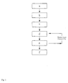
- Figure 1 shows the general steps in the fabrication of films by the technique described in this invention.
- the first steps, steps a b and c involve the selection of precursor compounds and the solvents.
- the selection of precursor compounds and the solvents is an important step in the preparation of thin films by chemical technique using precursor solution.
- the precursors for individual metal should have a long shelf life.
- the selected precursors should have high solubility in the selected solvents and the various solvents should be compatible when mixed.
- the final precursor solution should have a relatively long shelf life so that it can be made ahead of time in volume and used as needed.
- the various steps in the alkoxide-salt approach are :
- the procedure then consists of dissolving the individual precursors in the selected solvents and step d. involves the mixing of these solutions get a final homogeneous solution.
- the hydrolysis and polycondensation of the final solution is controlled to stabilize the final solution. This is usually performed with carboxylic acids, ⁇ -diketones, alcoholysis, and/or hydrolysis.
- the next step, e is the deposition of the precursor solution on a substrate.
- the films can be prepared from the precursor solution using spin, dip, or spray technique.
- Alcoholic solutions are generally capable of wetting all metal substrates, oxide substrates or metal-semiconductor substrates with a thin oxide layer on the surface. Almost any substrate that will support a thin film and is compatible with the materials and processes may be used.
- the thin films were prepared by using spin-coating technique, which is a well known form of deposition in which the precursor is placed on a wafer and the wafer is spun to evenly distribute the precursor over the wafer.
- the spinning speed and the viscosity of the solutions need to be optimized to control the thickness of the films.
- the wafer is spun at a spin rate of between 1000 rpm and 7000 rpm for a period of 5 seconds to 120 seconds.
- the film first produced on the substrate in step e is a wet film.
- the film is then baked for removal of organic content.
- the wafer is transferred to a hot plate on which it is baked.
- an oven may be used in baking if it is desirable to control ambients.
- the baking is at a temperature in the range 150-350 °C for a time period between 1-15 minutes.
- a drying step may be performed between the coating and the bake steps.
- the drying is performed between the temperature range 150-200 °C. If the desired thickness is not obtained in single coating, then the spin, dry, and bake processes, step e, are repeated till the desired thickness is achieved.
- step f after the last layer is coated and baked, the film is annealed in a diffusion furnace or in a rapid thermal annealing system. The annealing is preferably done at different temperatures for different times in an oxygen atmosphere at different flow rates. Depending on the type of substrate and the processing procedure, crystalline films with different morphologies can be obtained.
- polycrystalline film with no apparent preferred crystallographic orientations.
- Polycrystalline films are usually obtained when any one of the following substrate type is used: polycrystalline substrates, amorphous substrates, and single-crystal substrates with large lattice mismatch. Texture-oriented films may be obtained under several special conditions.
- the film grown over the surface may be highly preferentially oriented.
- the films can be grown with a preferred orientation if a small dc bias field is applied along the substrate surface during the post-deposition annealing treatment. The films annealed using rapid thermal annealing process also show preferred orientation for some cases.
- epitaxial films can be formed for some ferroelectric systems.
- the films of SrBi 2 Ta 2 O 9 were fabricated by the chemical precursor solution technique using room temperature solution preparation procedure as described.
- bismuth 2-ethylhexanoate, strontium acetate, and tantalum ethoxide were selected as precursors and acetic acid, 2-ethylhexanoic acid, and 2-methoxyethanol were selected as solvents.
- the selected precursors had high solubility in the corresponding solvents under ambient room temperature conditions.
- Bismuth 2-ethylhexanoate was dissolved in 2-ethylhexanoic acid, strontium acetate was dissolved in acetic acid, and a solution of tantalum ethoxide was formed in 2-methoxyethanol. Excess bismuth was added to account for the loss of bismuth during processing. The best results were obtained for 30 % excess bismuth. Then the various solutions were mixed together. The final solution was stable, clear, and transparent. The viscosity and surface tension of the solution was controlled by varying the 2-methoxyethanol content. The resulting films were annealed in the temperature range 600-750 °C in an oxygen atmosphere.
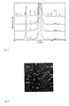
- Fig. 2 shows the x-ray diffraction patterns of the films.
- the films were found to be well crystallized at 650 °C with absence of any pyrochlore or secondary phases. As the annealing temperature was increased the peak intensity and sharpness in the x-ray diffraction pattern was found to increase indicating increase in grain sizes and crystallinity.
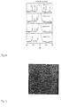
- Figure 3 shows the atomic force micrograph of the film annealed at 750 °C. The films exhibited a dense microstructure with no cracks or defects. The electrical characteristics were obtained on films in metal-ferroelectric film-metal (MFM) configuration.
- the MFM capacitors were prepared by depositing platinum electrodes through a mask on the top surface of the film by sputtering. The bottom platinum electrode was accessed by etching the film.
- the dielectric constant of the film annealed at 750 °C was found to be 330 at a frequency of 100 kHz.
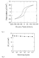
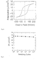
- Figure 4 shows the P-E hysteresis loop for the film annealed at 750 °C.
- a remanent polarization (2P r ) value of 17.2 ⁇ C/cm 2 and a coercive field value of 23 kV/cm was obtained for SrBi 2 Ta 2 O 9 thin films.
- the films showed good switching endurance, as shown in Fig. 5, under bipolar stressing at least up to 10 10 switching cycles.
- Bismuth 2-ethylhexanoate was dissolved in 2-ethylhexanoic acid, strontium acetate was dissolved in acetic acid, and a solution of tantalum ethoxide and titanium isopropoxide was formed in 2-methoxyethanol. Excess bismuth was added into the solution to account for bismuth loss during processing. Then the various solutions were mixed together. The final solution was stable, clear, and transparent. The viscosity and surface tension of the solution was controlled by varying the 2-methoxyethanol content.
- the present films, 0.7SrBi 2 Ta 2 O 9 -0.3Bi 3 TiTaO 9 composition were annealed in the temperature range 600-750 °C in an oxygen atmosphere. Fig.
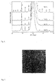
- FIG. 6 shows the x-ray diffraction patterns of the films.
- the films were found to be well crystallized at 600 °C with absence of any pyrochlore or secondary phases. As the annealing temperature was increased the peak intensity and sharpness in the x-ray diffraction pattern was found to increase indicating increase in grain sizes and crystallinity.
- Figure 7 shows the atomic force micrograph of the film annealed at 750 °C. The films exhibited a dense microstructure with no cracks or defects. The grain size was found to be much improved compared to SrBi 2 Ta 2 O 9 films annealed under similar conditions (Fig. 3). The electrical characteristics were obtained on films in metal-ferroelectric film-metal (MFM) configuration.
- MFM metal-ferroelectric film-metal
- the MFM capacitors were prepared by depositing platinum electrodes through a mask on the top surface of the film by sputtering. The bottom platinum electrode was accessed by etching the film.
- the dielectric constant of the film annealed at 750 °C was found to be 200 at a frequency of 100 kHz.
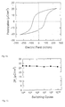
- Figure 8 shows the P-E hysteresis loop for the film annealed at 750 °C.
- a remanent polarization (2P r ) value of 27.8 ⁇ C/cm 2 and a coercive field value of 68 kV/cm was obtained for 0.7SrBi 2 Ta 2 O 9 -0.3Bi 3 TiTaO 9 thin films.
- the films annealed at 650 °C also exhibited much improved ferroelectric properties compared to SrBi 2 Ta 2 O 9 thin films (Table 1).
- the low temperature processing is desired as it will help in the selection of a suitable barrier layer for the memory device.
- the 2P r value was found to be significantly improved for the solid solution (Table 1).
- the films showed good switching endurance, as shown in Fig. 9, under bipolar stressing at least up to 10 10 switching cycles.
- Bismuth 2-ethylhexanoate was dissolved in 2-ethylhexanoic acid, strontium acetate was dissolved in acetic acid, and a solution of niobium ethoxide, tantalum ethoxide, and titanium isopropoxide was formed in 2-methoxyethanol. Excess bismuth was added into the solution to account for bismuth loss during processing. Then the various solutions were mixed together. The final solution was stable, clear, and transparent. The viscosity and surface tension of the solution was controlled by varying the 2-methoxyethanol content.
- the present films were annealed in the temperature range 600-750 °C in an oxygen atmosphere.
- Fig. 10 shows the x-ray diffraction patterns of the films. The films were found to be well crystallized at 600 °C with absence of any pyrochlore or secondary phases. As the annealing temperature was increased the peak intensity and sharpness in the x-ray diffraction pattern was found to increase indicating increase in grain sizes and cryst Hinity.
- Figure 11 shows the atomic force micrograph of the film annealed at 750 °C. The films exhibited a dense microstructure with no cracks or defects.
- the grain size was found to be much improved compared to SrBi 2 Ta 2 O 9 films annealed under similar conditions (Fig. 3).
- the electrical characteristics were obtained on films in metal-ferroelectric film-metal (MFM) configuration.
- the MFM capacitors were prepared by depositing platinum electrodes through a mask on the top surface of the film by sputtering. The bottom platinum electrode was accessed by etching the film.
- the dielectric constant of the film annealed at 750 °C was found to be 200 at a frequency of 100 kHz.
- Figure 12 shows the P-E hysteresis loop for the film annealed at 750 °C.
Description
- PZT based capacitors have larger polarization (40-50 µC/cm2) than the polycrystalline SBT-based capacitors (∼20 µC/cm2) hitherto developed.
- PZT layers with a pure perovskite structure and good electrical properties can be generally produces at lower temperatures (600-700 °C) than SBT layers (750-850 °C) depending on the particular film deposition technique.
- PZT based capacitors require oxide or hybrid-metal-oxide electrodes technology to yield negligible fatigue and imprint-two important electrical properties for FRAMs. These electrodes are more complicated to synthesize than pure metal electrodes such as Pt.
- PZT based capacitors involve Pb, which may present contamination and hazardous problems during fabrication.
- SBT based capacitors present negligible fatigue and imprint using the simpler Pt electrode technology.
- SBT layers maintain good electrical properties even when they are very thin (<100 nm).
- SBT based capacitors have lower polarization than PZT based capacitors. Intrinsic high polarization values may be necessary when scaling capacitors to the submicron dimensions needed for these memories. This may be a problem in relation to the application of SBT to high-density memories.
- The synthesis of SBT layers with the appropriate layered perovskite structure requires high temperature (800-850 °C) depending on the film deposition technique. The processing temperatures are high in relation to standard semiconductor device processing temperatures, and therefore efforts are warranted to reduce it.
- The Curie temperature of SBT is low (∼310 °C). A higher Curie temperature is desired for memory applications as the ferroelectric properties are strongly dependent on the Curie temperature. As the operating temperature approaches the Curie temperature the ferroelectric polarization decreases rapidly. So the Curie temperature is required to be much higher than the operating temperature range to ensure a stable constant polarization.
- SBT layers with an appropriate layered perovskite structure require high temperatures (800-850°C) depending on the film deposition technique. At lower temperatures the films exhibit poor microstructural and ferroelectric properties. The polycrystalline nature of the SBT layers in conjunction with the polarization direction of the SBT material may contribute to this effect. Intrinsic high polarization values may be necessary when scaling capacitors to the submicron dimensions needed for these memories. The idea of solid solution material to overcome these problems is based on the bulk ceramic approach where the properties of a material are modified by making a solid solution with a material having different micro structural and Curie temperature characteristics but similar structure (see E. C. Subbarao, supra). SBT has a curie temperature of 310°C while the Bi3TiTa1-yNbyO9 has Curie temperature in the range 870-950 °C. Both of these materials belong to the layered perovskite family. So the solid solution of these two materials is expected to exhibit a higher Curie temperature.
- For bulk SBT material a saturation polarization (Ps) of 5.8 µC/cm2 has been reported while a Ps value of 27.7 µC/cm2 has been reported for Bi3TiNbO9 material. So the solid solution is expected to show a higher polarization value compared to SBT.•It is not possible to reduce the post-deposition annealing temperature due to poor ferroelectric properties at lower annealing temperatures. This problem is intrinsic in nature and is due to small grain sizes at lower annealing temperatures. The Bi3TiTa1-yNbyO9 material shows a much larger grain structure compared to SBT under similar annealing conditions. So the solid solution is expected to yield larger grain sizes at lower annealing temperature compared to SBT and hence solve the problem of reducing the processing temperature.
| Improved Polarization for the novel solid solution material compared to SBT. | |||
| Temperature (°C) | SrBi2Ta2O9 thin films 2 Pr (µC/cm2) | 0.7SrBi2Ta2O9-0.3Bi3TiTaO9 thin films 2 Pr (µC/cm2) | 0.8SrBi2Ta2O9-0.2Bi3TiNbO9, thin films 2 pr (µC/cm2) |
| 650°C | 4.4 | 12.4 | 12.1 |
| 750 °C | 17.2 | 27.8 | 26.9 |
Claims (6)
- A method of forming a film of layered perovskite material, comprising the steps of(a) dissolving bismuth 2-ethylhexanoate in a first solvent to form a first solution;(b) dissolving strontium acetate in a second solvent to form a second solution;(c) dissolving titanium isopropoxide and tantalum ethoxide in a third solvent to form a third solution;(d) mixing together the solutions formed in steps (a), (b) and (c) to form a homogenous mixed solution, steps of (a), (b), (c) and (d) being carried out at ambient temperature; and(e) depositing the homogenous mixed solution onto a substrate, thereby to form a film, of (1-x)SrBi2TaO9-xBi3TiTaO9.
- A method of forming a film layered peroyskite material involving steps (a), (b) and (d) of claim 1, wherein a step (c) comprises dissolving titanium isopropoxide, tantalum ethoxide and niobium ethoxide in a third solvent to form a third solution and wherein a step (e) comprises depositing the homogenous mixed solution onto a substrate thereby to form a film of (1-x)SrBi2Ta2O9xBi3TiNbO9.
- A method according to any claim 1 or claim 2, further comprising the step of annealing the substrate and film at a temperature of 600-750°C.
- A method according to any one of claims 1 to 3, wherein the first solvent is 2-ethylhexanoic acid, the second solvent is acetic acid, and the third solvent is 2-methoxyethanol.
- A method according to any one of claims 1 to 4, wherein the amount of bismuth in step (a) is in a 30% stoichiometric excess.
- A method according to any one of claims 1 to 5, further comprising the step of forming a top electrode and a bottom electrode, sandwiching the film, whereby a capacitor structure is formed.
Applications Claiming Priority (2)
| Application Number | Priority Date | Filing Date | Title |
|---|---|---|---|
| US85225397A | 1997-05-06 | 1997-05-06 | |
| US852253 | 1997-05-06 |
Publications (2)
| Publication Number | Publication Date |
|---|---|
| EP0877100A1 EP0877100A1 (en) | 1998-11-11 |
| EP0877100B1 true EP0877100B1 (en) | 2001-06-20 |
Family
ID=25312854
Family Applications (1)
| Application Number | Title | Priority Date | Filing Date |
|---|---|---|---|
| EP98303376A Expired - Lifetime EP0877100B1 (en) | 1997-05-06 | 1998-04-30 | Process for fabricating solid-solution of layered perovskite materials |
Country Status (4)
| Country | Link |
|---|---|
| EP (1) | EP0877100B1 (en) |
| JP (1) | JPH1149600A (en) |
| KR (1) | KR100279228B1 (en) |
| DE (1) | DE69800954T2 (en) |
Families Citing this family (5)
| Publication number | Priority date | Publication date | Assignee | Title |
|---|---|---|---|---|
| DE19743269A1 (en) * | 1997-09-30 | 1999-04-01 | Siemens Ag | Manufacturing process for a bi-containing ceramic layer |
| US7476314B2 (en) | 2000-08-11 | 2009-01-13 | Reid Roger P | Keyed system for connection of filter cartridge to filter holder |
| US20060279901A1 (en) * | 2003-01-21 | 2006-12-14 | Yuki Miyamoto | Thin film capacitance element composition, high permittivity insulation film, thin film capacitance element, thin film multilayer capacitor and production method of thin film capacitance element |
| EP1591568A1 (en) * | 2003-01-21 | 2005-11-02 | TDK Corporation | Composition for thin film capacitance element, insulating film of high dielectric constant, thin film capacitance element, thin film laminated capacitor and method for manufacturing thin film capacitance element |
| CN114956816B (en) * | 2022-06-07 | 2023-03-24 | 清华大学 | High-performance pyrochlore energy storage ceramic material and preparation method and application thereof |
Family Cites Families (3)
| Publication number | Priority date | Publication date | Assignee | Title |
|---|---|---|---|---|
| US5423285A (en) * | 1991-02-25 | 1995-06-13 | Olympus Optical Co., Ltd. | Process for fabricating materials for ferroelectric, high dielectric constant, and integrated circuit applications |
| US5468679A (en) * | 1991-02-25 | 1995-11-21 | Symetrix Corporation | Process for fabricating materials for ferroelectric, high dielectric constant, and integrated circuit applications |
| US5508226A (en) * | 1991-12-13 | 1996-04-16 | Symetrix Corporation | Low temperature process for fabricating layered superlattice materialsand making electronic devices including same |
-
1998
- 1998-04-30 EP EP98303376A patent/EP0877100B1/en not_active Expired - Lifetime
- 1998-04-30 DE DE69800954T patent/DE69800954T2/en not_active Expired - Lifetime
- 1998-04-30 JP JP10120924A patent/JPH1149600A/en not_active Withdrawn
- 1998-05-06 KR KR1019980016847A patent/KR100279228B1/en not_active IP Right Cessation
Also Published As
| Publication number | Publication date |
|---|---|
| KR100279228B1 (en) | 2001-02-01 |
| JPH1149600A (en) | 1999-02-23 |
| KR19980086940A (en) | 1998-12-05 |
| EP0877100A1 (en) | 1998-11-11 |
| DE69800954T2 (en) | 2001-11-22 |
| DE69800954D1 (en) | 2001-07-26 |
Similar Documents
| Publication | Publication Date | Title |
|---|---|---|
| US5434102A (en) | Process for fabricating layered superlattice materials and making electronic devices including same | |
| US5514822A (en) | Precursors and processes for making metal oxides | |
| JP4905620B2 (en) | Ceramics and manufacturing method thereof, semiconductor device, actuator, optical modulator, ultrasonic sensor | |
| Vorotilov et al. | Sol-gel derived ferroelectric thin films: Avenues for control of microstructural and electric properties | |
| US6072207A (en) | Process for fabricating layered superlattice materials and making electronic devices including same | |
| EP0890980A2 (en) | Method of making integrated circuit capacitors | |
| EP0665981B1 (en) | Process for fabricating layered superlattice materials and electronic devices including same | |
| US5559260A (en) | Precursors and processes for making metal oxides | |
| US5601869A (en) | Metal polyoxyalkylated precursor solutions in an octane solvent and method of making the same | |
| US6174564B1 (en) | Method of making metal polyoxyalkylated precursor solutions | |
| JP2003002647A (en) | Plzt ferroelectric thin film, composition for forming the same, and producing method for the same | |
| Kim et al. | The effects of PbTiO3 thin template layer and Pt/RuO2 hybrid electrode on the ferroelectric properties of sol-gel derived PZT thin film | |
| EP0877100B1 (en) | Process for fabricating solid-solution of layered perovskite materials | |
| KR100346900B1 (en) | Solution of metal polyoxyalkylated precursors dispersed in octane solvent, process for producing precursor solution and process for producing thin film for integrated circuit using this precursor solution | |
| JP2000188377A (en) | Ferroelectric thin-film element and its manufacture | |
| Paik et al. | Sol-gel fabrication of nanocomposites: Alternate thin layers of PbTiO3 and PbZrO3 | |
| JPH06314794A (en) | Electronic device and manufacture thereof | |
| Kosec et al. | 4.1. 7 FERROELECTRIC THIN FILMS |
Legal Events
| Date | Code | Title | Description |
|---|---|---|---|
| PUAI | Public reference made under article 153(3) epc to a published international application that has entered the european phase |
Free format text: ORIGINAL CODE: 0009012 |
|
| AK | Designated contracting states |
Kind code of ref document: A1 Designated state(s): DE FR GB |
|
| AX | Request for extension of the european patent |
Free format text: AL;LT;LV;MK;RO;SI |
|
| 17P | Request for examination filed |
Effective date: 19990422 |
|
| AKX | Designation fees paid |
Free format text: DE FR GB |
|
| 17Q | First examination report despatched |
Effective date: 20000120 |
|
| GRAG | Despatch of communication of intention to grant |
Free format text: ORIGINAL CODE: EPIDOS AGRA |
|
| GRAG | Despatch of communication of intention to grant |
Free format text: ORIGINAL CODE: EPIDOS AGRA |
|
| GRAH | Despatch of communication of intention to grant a patent |
Free format text: ORIGINAL CODE: EPIDOS IGRA |
|
| GRAH | Despatch of communication of intention to grant a patent |
Free format text: ORIGINAL CODE: EPIDOS IGRA |
|
| GRAA | (expected) grant |
Free format text: ORIGINAL CODE: 0009210 |
|
| AK | Designated contracting states |
Kind code of ref document: B1 Designated state(s): DE FR GB |
|
| REF | Corresponds to: |
Ref document number: 69800954 Country of ref document: DE Date of ref document: 20010726 |
|
| ET | Fr: translation filed | ||
| REG | Reference to a national code |
Ref country code: GB Ref legal event code: IF02 |
|
| PLBE | No opposition filed within time limit |
Free format text: ORIGINAL CODE: 0009261 |
|
| STAA | Information on the status of an ep patent application or granted ep patent |
Free format text: STATUS: NO OPPOSITION FILED WITHIN TIME LIMIT |
|
| 26N | No opposition filed | ||
| REG | Reference to a national code |
Ref country code: FR Ref legal event code: PLFP Year of fee payment: 19 |
|
| REG | Reference to a national code |
Ref country code: FR Ref legal event code: PLFP Year of fee payment: 20 |
|
| PGFP | Annual fee paid to national office [announced via postgrant information from national office to epo] |
Ref country code: GB Payment date: 20170419 Year of fee payment: 20 Ref country code: FR Payment date: 20170419 Year of fee payment: 20 Ref country code: DE Payment date: 20170419 Year of fee payment: 20 |
|
| REG | Reference to a national code |
Ref country code: DE Ref legal event code: R071 Ref document number: 69800954 Country of ref document: DE |
|
| REG | Reference to a national code |
Ref country code: GB Ref legal event code: PE20 Expiry date: 20180429 |
|
| PG25 | Lapsed in a contracting state [announced via postgrant information from national office to epo] |
Ref country code: GB Free format text: LAPSE BECAUSE OF EXPIRATION OF PROTECTION Effective date: 20180429 |