EP0875902A2 - Enhanced signal processing random access memory device utilizing a DRAM memory array integrated with an associated SRAM cache and internal refresh control - Google Patents
Enhanced signal processing random access memory device utilizing a DRAM memory array integrated with an associated SRAM cache and internal refresh control Download PDFInfo
- Publication number
- EP0875902A2 EP0875902A2 EP98303023A EP98303023A EP0875902A2 EP 0875902 A2 EP0875902 A2 EP 0875902A2 EP 98303023 A EP98303023 A EP 98303023A EP 98303023 A EP98303023 A EP 98303023A EP 0875902 A2 EP0875902 A2 EP 0875902A2
- Authority
- EP
- European Patent Office
- Prior art keywords
- memory
- address
- memory array
- memory device
- refresh
- Prior art date
- Legal status (The legal status is an assumption and is not a legal conclusion. Google has not performed a legal analysis and makes no representation as to the accuracy of the status listed.)
- Withdrawn
Links
- 238000000034 method Methods 0.000 claims description 14
- 230000004044 response Effects 0.000 claims description 7
- 230000003068 static effect Effects 0.000 claims description 5
- 239000000725 suspension Substances 0.000 claims description 3
- 230000008878 coupling Effects 0.000 claims 2
- 238000010168 coupling process Methods 0.000 claims 2
- 238000005859 coupling reaction Methods 0.000 claims 2
- 230000003213 activating effect Effects 0.000 claims 1
- 235000019800 disodium phosphate Nutrition 0.000 description 12
- 238000010586 diagram Methods 0.000 description 11
- 230000006870 function Effects 0.000 description 6
- 230000008569 process Effects 0.000 description 5
- 230000003111 delayed effect Effects 0.000 description 4
- 230000000694 effects Effects 0.000 description 4
- 238000005516 engineering process Methods 0.000 description 3
- 230000004048 modification Effects 0.000 description 3
- 238000012986 modification Methods 0.000 description 3
- 230000008859 change Effects 0.000 description 2
- 230000001934 delay Effects 0.000 description 2
- 230000014759 maintenance of location Effects 0.000 description 2
- 239000008186 active pharmaceutical agent Substances 0.000 description 1
- 238000003491 array Methods 0.000 description 1
- 230000002457 bidirectional effect Effects 0.000 description 1
- 239000003990 capacitor Substances 0.000 description 1
- 239000000470 constituent Substances 0.000 description 1
- 230000002349 favourable effect Effects 0.000 description 1
- 230000010354 integration Effects 0.000 description 1
- 230000000737 periodic effect Effects 0.000 description 1
- 230000000630 rising effect Effects 0.000 description 1
Images


Classifications
-
- G—PHYSICS
- G11—INFORMATION STORAGE
- G11C—STATIC STORES
- G11C11/00—Digital stores characterised by the use of particular electric or magnetic storage elements; Storage elements therefor
- G11C11/21—Digital stores characterised by the use of particular electric or magnetic storage elements; Storage elements therefor using electric elements
- G11C11/34—Digital stores characterised by the use of particular electric or magnetic storage elements; Storage elements therefor using electric elements using semiconductor devices
- G11C11/40—Digital stores characterised by the use of particular electric or magnetic storage elements; Storage elements therefor using electric elements using semiconductor devices using transistors
- G11C11/401—Digital stores characterised by the use of particular electric or magnetic storage elements; Storage elements therefor using electric elements using semiconductor devices using transistors forming cells needing refreshing or charge regeneration, i.e. dynamic cells
- G11C11/406—Management or control of the refreshing or charge-regeneration cycles
Definitions
- the present invention is related to the subject matter of United States Patent Application Serial No. 08/319,289 filed October 6, 1994 (U.S. Patent No. 5,699,317) and 08/460,665 filed June 2, 1995 (U.S. Patent No. 5,721,862), both assigned to Enhanced Memory Systems, Inc., a subsidiary of Ramtron International Corporation, Colorado Springs, Colorado, the disclosures of which are herein specifically incorporated by this reference.
- the present invention relates, in general, to the field of integrated circuit (“IC”) memory devices. More particularly, the present invention relates to a highly integrated enhanced signal processing random access memory IC device which utilizes a dynamic random access memory (“DRAM”) primary memory in conjunction with a static random access memory (“SRAM”) cache and on-chip refresh control function which may be conveniently supplied in an industry standard SRAM IC pin-out.
- DRAM dynamic random access memory
- SRAM static random access memory
- DSP Digital signal processing
- DSP Digital signal processing
- analog signal processing performed digitally or real-time signal processing as opposed to processing performed off-line.
- DSP is a highly computationally intensive form of signal processing in which many arithmetic operations must be performed very rapidly.
- the choice and configuration of DSP memory components for such high throughput processing gives rise to numerous unique considerations. Among these are that the individual memory devices, or "chips" which must be addressed by the DSP components must match the overall system speed or constitute a data processing "bottleneck”.
- the present invention advantageously provides a memory device utilizing a high density DRAM core memory array integrated with an SRAM cache and internal refresh control functionality which may be provided in an integrated circuit package which is pin-compatible with industry standard SRAM memory devices.
- the memory device of the present invention provides a high speed memory access device of particular utility in conjunction with DSP processors with performance equivalent to that of SRAM memory devices but requiring a significantly small die size which allows for the provision of greater effective memory capacity per die area.
- the internal refresh functionality of the device provides for all refresh operations to the DRAM memory array to occur transparently to the device user and provides control signals alerting the associated controller when refresh operations are being performed.
- a refresh control technique for a memory device incorporating a DRAM memory array which comprises the steps of periodically refreshing the memory array if an external input to the memory device is in a first state thereof; delaying at least one type of access to the memory device during the step of periodically refreshing the memory array for a predetermined time period; and asserting a wait signal on an external output of the memory device in response to the step of delaying.
- the refresh control technique comprises the steps of suspending the step of periodically refreshing the memory array if the external input to the memory device is in a second opposite state thereof; maintaining suspension of the step of periodically refreshing the memory array until a predetermined number of refresh operations have been suspended; and performing a refresh operation to the memory array if the predetermined number of suspended refresh operations is reached.
- an integrated circuit memory device which comprises a dynamic random access memory array, a static random access memory cache coupled to the memory array for receiving a row of data therefrom and a memory decoder coupled to the memory array and the memory cache.
- An input/output control circuit is coupled to the memory array and the memory cache and an external address bus is coupled to the memory decoder for accessing the memory array and the memory cache.
- An external data bus is bidirectionally coupled to the input/output control circuit for receiving data to be written to the memory array at a location determined by the memory decoder and for providing data to be read from the memory cache and an external address valid strobe input is coupled to the memory decoder for indicating that an address signal on the external address bus is valid.
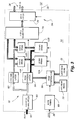
- the memory device 10 comprises, in pertinent part, a dynamic random access memory (“DRAM”) array 12 comprising one or more banks of DRAM memory and an associated static random access memory (“SRAM”) cache 14 also comprising one or more corresponding banks of SRAM memory.
- DRAM dynamic random access memory
- SRAM static random access memory
- the memory device 10 is accessed by means of a parallel address bus 16, which in the exemplary 1Mb (64K x 16) device illustrated, comprises sixteen address lines A 0 through A 15 .
- the address bus 16 provides address signal inputs to the DRAM array 12 and the SRAM cache 14 through a memory decoder 18 which also has as inputs an address valid strobe input (“ASTB ⁇ ") 20, a write enable input (“WE ⁇ ”) 22 and a chip enable input (“CE ⁇ ”) 24 as will be more fully described hereinafter.
- a wait-state generator 28 is coupled to an additional output of the memory decoder 18 and provides a "Wait” output signal on output 30 of the memory device 10.
- An output enable input (“OE ⁇ ") 32 is also supplied to the memory device 10 for input to an input/output (“I/O") control block 34 which is bidirectionally coupled via an internal data bus to the DRAM array 12 and the SRAM cache 14 such that data may be read from, or written to, the memory device 10 via a bidirectional data bus 36.
- the data bus 36 comprises sixteen I/O pins denominated DQ O through DQ 15 .
- the memory device 10 of Fig. 1 is illustrated in an exemplary industry standard 64K x 16 SRAM pin-out.
- the memory device 10 may be conveniently encapsulated in any pin-out or package configuration including a 44 pin TSOP or the SOJ package as shown.
- Any number of industry standard SRAM pin-outs i.e. 20, 22, 24, 28, 32, 36, 44, 50, 52, 64, 68 and the like
- any type of package i.e. DIP, ZIP, PLCC, PQFP, SOJ, TSOP, SOIC, SIMM and the like
- the memory device 10 is shown having additional pins corresponding to: a sleep input 42 which causes the memory device 10 to power down internally; an upper byte enable input (“UB ⁇ ”) 44 and lower byte enable input (“LB ⁇ ”) 46 which have equivalent functions as to the CE ⁇ input 24 with respect to the upper and lower 8 bits of data on the data bus respectively; and power supply (“VDD”) 48 and ground (“GND”) 50 inputs to provide operating power to the memory device 10, all as will be more fully described hereinafter.
- a sleep input 42 which causes the memory device 10 to power down internally
- U ⁇ upper byte enable input
- LB ⁇ lower byte enable input
- VDD power supply
- GND ground
- the memory device 10 which may comprise a monolithically integrated circuit in a preferred embodiment, may incorporate, as shown, two or more banks of DRAM memory comprising arrays 12A and 12B and two or more banks of SRAM memory comprising corresponding caches 14A and 14B.
- the memory decoder 18 (Fig. 1) is shown as comprising an address demultiplexer 60 and separate column and row address latches 62 and 64 respectively.
- the address demultiplexer 60 and column and row address latches 62, 64 serve to derive the location within the DRAM array 12A and 12B wherein data is to be written, or from which data is to be read from the associated SRAM cache 14A and 14B as loaded from the DRAM array 12A and 12B as determined by the signals on the address bus 16.
- a row comparator 66 is coupled to an output of the row address latch and to a pair of last row read registers 70, 72 (or any other number of registers corresponding to the number of banks of the DRAM array 12A and 12B and SRAM cache 14A and 14B).
- the last row read registers 70, 72 serve to maintain the row address of the data that is currently maintained within the SRAM memory comprising SRAM cache 14A and 14B.
- the appropriate bank is selected by the 1 of 2 selector 74 under control of the row address latch 64 and latched into a data latch 76 for output on the data bus 36.
- the associated DRAM array 12A and 12B loads the next row to the SRAM cache 14. If the intended read access is a cache "miss” then the data is read out of the appropriate row of the DRAM array 12A and 12B to the SRAM cache 14A and 14B and all subsequent reads are then from the SRAM cache 14A and 14B.
- the access is a write operation to a cache "hit"
- the data on the data bus 36 is written both to the DRAM array 12A and 12B as well as to the SRAM cache 14A and 14B.
- the access is a cache "miss', then data is written solely to the DRAM array 12A and 12B.
- all reads are from the SRAM cache 14A and 14B and all writes are to the DRAM array 12A and 12B with a write-through to the SRAM cache 14A and 14B if a cache "hit" as indicated by the appropriate one of the last row read registers 70, 72.
- the embodiment of the memory device 10 above described provides a cost effective 1 Mb pin compatible SRAM equivalent integrated circuit of particular utility in conjunction with DSP and other high performance systems and broadens the options for system designers who have previously used DRAM for low cost memory and expensive SRAM for high performance.
- the memory device 10 melds these separate technologies to create a cost effective memory with an effective 10 nS access time. It is of particular utility in solving the memory problems of high performance systems without regard to rigid memory classifications by combining an appropriate amount of different memory technologies and logic.
- the memory device 10 provides a standard SRAM pin out with the unused pins allocated to address strobe and wait signals.
- the address strobe input allows an memory device 10 to interface with TMS320 (available from Texas Instruments, Inc., Dallas, Texas) and other processors to provide optimal timing with a glueless interface.
- TMS320 available from Texas Instruments, Inc., Dallas, Texas
- the wait signal indicates that the memory device 10 cannot provide zero wait state operation for high speed systems and is typically connected to the ready input of a processor.
- the memory device 10 provides a cost-effective high performance memory for digital signal processing and other high performance applications. It achieves these goals by using a fast DRAM array 12 (divided into one or more banks) as the bulk memory and dynamically allocating a very fast SRAM cache 14 (also divided into one or more cache lines) to the memory area that is being used.
- the memory device 10 provides a non-multiplexed SRAM like addressing scheme. Since the core DRAM memory array 12 is constructed from DRAM, a random read operation will access the DRAM array 12. An entire DRAM row of 1K-bits will automatically be loaded into very fast SRAM cache. Subsequent accesses that fall within the 64-word address range of the DRAM row will be made in SRAM at high speed. These addresses are called in-page accesses. Addresses that are not in-page will cause a DRAM access and a new row will be loaded into SRAM. In-page accesses are performed in 10 nS for zero wait state operation and the wait signal on the wait output 30 is not asserted. Accesses that are out-of-page and cause a DRAM array 12 access will cause a wait state via the wait signal on the wait output 30 This scheme applies to reads and writes equally.
- the memory device 10 will perform most accesses in 10 nS. However, the actual performance level will depend on the application and the percentage of data that occurs in blocks. Since the core memory array is DRAM, it must be refreshed and on-chip logic supervises this function. If an out-of-page access occurs during a DRAM refresh operation, the wait signal on the wait output 30 will be asserted. Refresh logic is optimized to cause minimum delays by performing refreshes while in page accesses are being done.
- FIG. 3 illustrates the elements of a memory device 10.including the presence of 2 SRAM caches 14A and 14B. This scheme increases the likelihood of a random in-page access and also allows intelligent planning of SRAM access.
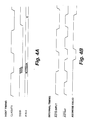
- Figs. 4A and 4B the address decoding operations for the memory device 10 of the preceding figures is shown.
- memory is either fast (SRAM) or slow (DRAM), and the latter, slow memory inserts wait states all of the time. Fast memory never inserts wait states.
- SRAM fast
- DRAM slow
- the memory dynamically changes between fast and slow based on the address.
- the address map is not fixed, with fast memory in certain addresses and slow in others. In fact, the memory can be fast over almost the entire memory map. For this reason, proper address decoding is an important aspect in the function of the memory device 10.
- Combining mixed memory technologies in a seamless solution requires the memory to be aware of the address space and to manage access based on addresses.
- the memory device 10 monitors addresses in order to determine if an access is required to the DRAM array 12 or the SRAM cache 14. Each address is broken into its constituent row and column portions and is latched internally.
- the lower 6 address lines AO-A5 of the address bus 16 are column addresses. They designate the location of the SRAM that is used and correspond to the DRAM array 12 columns.
- the upper 10 address lines A6-A 15 of the address bus 16 are row addresses. They designate the DRAM array 12 row that is accessed and loaded into the SRAM cache 14. Since the DRAM array 12 is split into 2 banks,(12A and 12B) the address A6 is also a DRAM bank select. Each DRAM bank (12A or 12B) has an associated SRAM cache (14A or 14B), so A6 selects which of the two 64 x 16 SRAM caches 14A or 14B are used.
- Row addresses in each bank are compared against the last row read holding registers 70, 72 (one for each bank). If a row address, that is the upper 10-bits of address, is the same as the previous access, then the access is performed in the SRAM cache 14A or 14B at high speed. If the row address has changed, then the DRAM array 12A or 12B is accessed and loaded into the corresponding SRAM cache 14A or 14B.
- the address is latched and processed.
- the memory In order to provide fast access, the memory must know that the address is valid.
- the ASTB ⁇ address strobe input 20 signal provides this information.
- two exemplary embodiments of the memory device 10 are contemplated and shown.
- the host processor does not generate an address valid strobe.
- the ASTB ⁇ input 20 signal comes from a processor clock. Since addresses are valid after the clock edge, the signal is delayed internally in proportion to the clock frequency.
- This version interfaces directly to the TMS320C3X and TMS320C5X series DSPs available from Texas Instruments, Inc..
- a true address valid signal is provided by the processor or system to the ASTB ⁇ input 20 and is used by the memory device 10 without delay, and the figure illustrates the usage of the address valid strobe.
- the memory device 10 provides in-page access time at 10 nS.
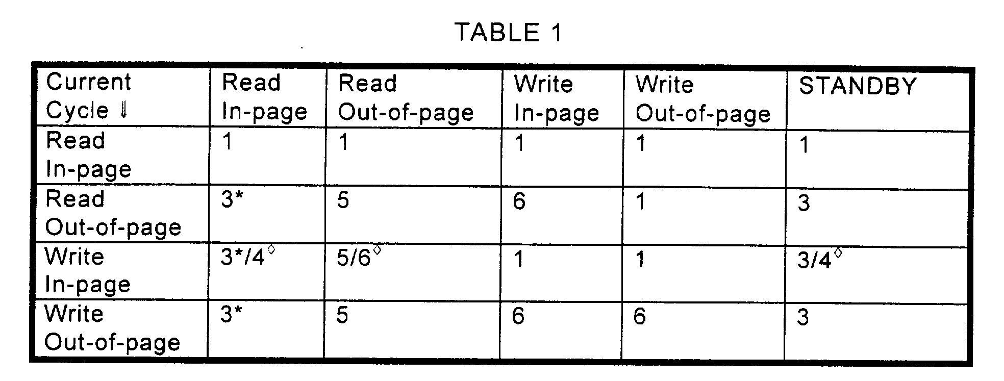
- the actual system timing for each memory cycle depends on the type of cycle. There are four basic types of cycles as shown in the following Table 1. The timing of each also depends on the cycle that preceded it.
- the first criteria is whether the access is in-page or out- of-page.
- An in-page access is one where the current row address (A6-A 15) corresponds to the last row read (in one of two banks of SRAM cache 14A or 14B). This means that the memory is available in SRAM for high speed access. In general, in-page access is associated with zero wait state operation and out-of-page access requires wait states.
- the second criteria is whether the access is a read or a write.
- address lines A6-A 15 are compared to the last row read register(s) 70, 72. If they match, then the requested address currently resides in the SRAM cache 14A or 14B regardless of the state of A5- AO. This is called an in-page access.
- Read accesses to in-page addresses can be performed in 10 nS. Since a single page contains 64 words, it is possible to perform as many as 64 consecutive reads, each in 10 nS once the row is loaded.
- an out-of-page read is performed.
- the out-of-page read involves an access to the DRAM array 12A and 12B. The entire row is loaded into the corresponding SRAM cache 14A or 14B. Since the DRAM array 12 is accessed, the first access requires extra time. Therefore, the wait signal on the wait output 30 will be asserted until the data has been loaded into the SRAM cache 14 and high speed access is available. The number of waits generated by this activity depends on the actual processor bus speed.
- the system performs one out-of-page read followed by seven in-page reads.
- a page may be though of as a 64-word high speed working area.
- Fig. 3 illustrates read access for both out-of-page and in-page accesses using a TMS320C3x or TMS320C5x host processor. Detailed timing is described and shown in more detail hereinafter.
- the write operation requires opening the DRAM page. This operation requires longer than accessing an open array. Therefore, the write access will cause the wait signal to be invoked on the wait output 30.
- in-page reads can occur during an out-of-page read cycle. While an out-of-page read may have a 50 nS cycle time, a new in-page read may be performed 30 nS into the out-of-page cycle. Thus in order to understand access times, the previous cycle should be considered.
- Table 1 illustrates the system timing for various combinations. Note that the timings notations assume a 10 nS access and cycle times are standard. Thus when the table specifies 3 cycles, this means 30 nS which may be only one bus cycle for a given processor. Certainly if a system is running slower than 10 nS, the number of wait states will be lower.
- Wait states are a result of the DRAM array 12 timing.
- SRAM cache 14 accesses occur in one cycle. 3 cycle accesses occur when the DRAM array 12 must be opened, where it was already closed. 5 cycle accesses occur when a DRAM page must be closed prior to opening a new DRAM page. A 6 cycle access can occur because a DRAM page is held open in-case of back-to-back write operations. This achieves 1-cycle access for in-page writes following writes.
- All DRAM array 12 aspects are transparent to the user. They will simply result in wait-states being generated to accommodate different address sequences and it should be noted that the number of cycles indicated reflects 10 nS cycles. A slower processor would receive less wait states.
- the 1 Mb DRAM array 12 must be refreshed, and the memory device 10 supervises its own refresh activity.
- these refreshes can be hidden so that they do not impact access time.
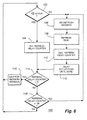
- the logic flow chart of Fig. 6 illustrates the algorithm used by the refresh controller.
- the refresh process 100 begins with decision step 102 to determine if the CE ⁇ input 24 to the memory device 10 is active. If it is, then the internal refresh delay counter is incremented. If the CE ⁇ signal has not been asserted, the process 100 proceeds to step 106 to increment the refresh address and then to step 108 to refresh the appropriate row in the DRAM array 12. Thereafter, at step 110 the refresh delay counter is decremented and any out-of-page operation is delayed until it is completed at step 112.
- step 114 determines if the refresh delay counter is zero. If it is, then at step 116 a wait is entered for a refresh interval and the process returns back to decision step 102. On the other hand, if the refresh delay counter is not zero, then, at decision step 118 the refresh delay counter is tested to see if it is equal to 128. If it is, then the process returns to step 106. Otherwise, it returns to decision step 102.
- the refresh controller will attempt to perform a refresh. If the memory device 10 is not busy. i.e. CE ⁇ is inactive, the refresh will occur. After its beginning, a refresh causes a 55 nS delay in the memory device's ability to perform an out-of-page access. An in-page read access will occur without delay. If an out-of-page access is attempted while a refresh is ongoing, the wait signal will be asserted on the wait output 30.
- the refresh controller is designed to accommodate two schemes. First is a system that maintains a continuous level of activity that can afford a 55 nS delay every 125 uS. In this case, one access will cause an extra 1-2 wait states every 125 uS. Most systems can afford this delay.
- Second is a system with bursts of high intensity activity that can not be interrupted followed by longer periods of STANDBY time.
- the user prevents delays by holding the CE ⁇ signal active during periods that can not be delayed. Many processors do this automatically.
- CE ⁇ is active, a refresh will not be performed until 128 have been missed, which takes 16 mS.
- the memory device 10 will begin to perform refreshes. The longest sequential delay will be 128 refreshes or 7 uS after a user invoked delay of 16 mS.
- the memory device 10 When the CE ⁇ signal is not active, the memory device 10 is in a STANDBY state. As shown in Table 1 above, from a timing perspective a STANDBY cycle is the same as an in-page read cycle. This is because the DRAM array 12 will be closed and the precharge delay satisfied. A STANDBY condition corresponds to standby in an SRAM device except that distributed refreshes will occur. These cause active-current spikes approximately every 125 uS but a low average power consumption will be achieved.
- the memory device 10 also incorporates a SLEEP mode pin 42. It is located on an unused pin in the standard SRAM pin configuration.
- the SLEEP signal indicates that a long period of STANDBY time is expected.
- SLEEP powers down the memory device 10, including refresh, allowing a very low current with no spikes.
- SLEEP mode will not provide data retention so it may be used when the data in memory is no longer needed after the SLEEP mode is removed.
- Active low signal that indicates the memory cycle is a write operation.
- An early write which offers more favorable timing will occur when WE ⁇ is asserted prior to CE ⁇ .
- a late write which occurs when WE ⁇ falls after CE ⁇ is acceptable.
- This signal indicates that the memory cannot provide high speed access for the requested memory cycle. It will be driven high until the memory can provide such high speed access.
- the ASTB is expected to be derived from a processor clock, where the falling edges occur prior to a valid address. Internally, the ASTB input is delayed by 1 ⁇ 4 of a duty cycle prior to latching the address.
- a rising edge on this signal indicates that the address is valid. No delay is applied, not that the polarity is reversed.
- This active high signal causes the DM2104 to power down internally. No data retention is guaranteed so this mode is best used when a task is complete and the memory will not be used for an extended period.
- SLEEP mode produces much lower power consumption than standby mode.
- Active low signal that indicates that the memory should drive the data bus.
- OE ⁇ When OE ⁇ is high, the data bus is tristate.
- UB ⁇ has an equivalent function to CE ⁇ except only as regards the upper 8-bits of the data bus. UB ⁇ must be low in order to access the upper byte of the data bus.
- LB ⁇ has an equivalent function to CE ⁇ except only as regards the lower 8.bits of the data bus. LB ⁇ must be low in order to access the upper byte of the data bus.
- a 15-A6 specify the memory row, with A6 being a bank select.
- A5-A0 specify the column and SRAM location.
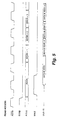
- ASTB timing diagrams are shown for two possible implementations of the memory device 10 of the present invention showing the interrelationship among the ASTB ⁇ input 20, address bus 16 and CE ⁇ input 24.
- Table 3 AC Read Parameters
- Table 4 AC Write Parameters
- AC Read Parameters...TA -40°C to +85°C
- VCC 4.5V to 5.5V
- C1 50 pF
- Symbol Parameter MIN MA X Units Notes t ARA1 In-page Access from Address Valid 10 nS t ARA0 Out-of-Page Access from Address Valid 30 nS t RC1 In-page Read Cycle Time 10 nS t RCO Out-of-page Read Cycle Time 50 nS t AST1 Address Setup to ASTB falling (Example 1) -1 ⁇ 4 t ASTB cycle *1 t AST2 Address Setup to ASTB falling (Example 1) -1 ⁇ 4 t ASTB cycle *1 t AST2 Address Setup to ASTB falling (Ex
- - In-page read cycles may occur after the out-of-page read access time has been satisfied without regard to the out-of-page cycle time. Other cycles must satisfy the read cycle time prior to beginning. 2.
- the ASTB is assumed periodic. The Address is expected after the ASTB falling edge, but no later than 1 ⁇ 4 clock cycle.
- In-page write cycles that occur following reads may be posted in 10 nS (access time) must the following cycle must delay until the Write Cycle time is satisfied.
- In-page writes that occur following other write operations occur in 10 nS but one write cycle time must be met prior to beginning a read or an out-of-page write.
- An early write indication (WE before ASTB) will change this specification to 50 nS.
- In-page write or read cycles may occur after the out-of-page write access time has been satisfied without regard to the out-of-page cycle time. Other cycles must satisfy the write cycle time prior to beginning. 4.
- An early write indication (WE before ASTB) will change this specification to 50 nS.
- Fig. 9A the memory device 10 read timing
- Fig. 9B write timing
- Fig. 9C sleep timing
- the read timing of Fig. 9A illustrates the functional and timing interrelationship amongst the ASTB ⁇ input 20; the CE ⁇ input 24; UB ⁇ and LB ⁇ inputs 44, 46; the address bus 16; the data bus 36; OE ⁇ input 32 and the wait output 30.
- the write timing diagram of Fig. 9B illustrates the functional and timing interrelationship amongst the ASTB ⁇ input 20; the CE ⁇ input 24; the UB ⁇ and LB ⁇ inputs 44, 46; the address bus 16, the WE ⁇ input 22 and data in and data out on the data bus 36.
- the sleep timing diagram of Fig. 9C illustrates the functional and timing interrelationship amongst the ASTB ⁇ input 20; the CE ⁇ input 24; the UB ⁇ and LB ⁇ inputs 44, 46; the address bus 16; the data bus 36 and the wait output 30.
- an enhanced digital signal processing random access memory device utilizing a highly density DRAM core memory array integrated with an SRAM cache and internal refresh control functionality which may be provided in an integrated circuit package which is pin-compatible with industry standard SRAM memory devices.
- the memory device provides a high speed memory access device of particular utility in conjunction with DSP processors with performance equivalent to that of SRAM memory devices but requiring a significantly small die size which allows for the provision of greater effective memory capacity per die area.
- the internal refresh functionality of the device provides for all refresh operations to the DRAM memory array to occur transparently to the device user and provides control signals alerting the associated controller when refresh operations are being performed.
Landscapes
- Engineering & Computer Science (AREA)
- Microelectronics & Electronic Packaging (AREA)
- Computer Hardware Design (AREA)
- Dram (AREA)
- Static Random-Access Memory (AREA)
Abstract
Description
With reference additionally now to Figs. 4A and 4B, the address decoding operations for the
Since the
| S | RM | RH | RH | RH | RM | RM | RH | RH | RM | RH | RM | |
| - | 3 | 1 | 1 | 1 | 3 | 5 | 1 | 1 | 3 | 1 | 4 | |
| S | WM | WH | WH | WH | WM | WM | WH | WH | WM | WH | WM | |
| - | 3 | 1 | 1 | 1 | 6 | 6 | 1 | 1 | 6 | 1 | 6 | |
| S | RH | WH | RM | WM | RH | WM | RM | WH | RH | WH | WH | RM |
| - | 1 | 3 | 6 | 5 | 1 | 3 | 6 | 5 | 1 | 3 | 1 | 6 |
| *Note S = Standby, RH = Read in-page, RM = Read out-of-page, WH = Write in-page, and WM = Write out-of-page |
| AC Read Parameters...TA=-40°C to +85°C, VCC=4.5V to 5.5V, C1=50 pF | |||||
| Symbol | Parameter | MIN | MA X | Units | Notes |
| tARA1 | In-page Access from | 10 | nS | ||
| tARA0 | Out-of-Page Access from | 30 | nS | ||
| tRC1 | In-page | 10 | nS | ||
| tRCO | Out-of-page | 50 | nS | ||
| tAST1 | Address Setup to ASTB falling (Example 1) | -¼ | tASTB cycle | *1 | |
| tAST2 | Address Setup to ASTB falling (Example 2) | 0 | nS | *2 | |
| tCST | CE Setup to ASTB falling | 0 | |||
| tASTB | ASTB cycle time | 25 | nS | ||
| tCA | Access time from CE, UB, LB | 10 | |||
| tCOE | Output Enable from CE | 5 | nS | ||
| tOE | Output Enable from OE | 5 | nS | ||
| tCOD | Output Disable from CE, UB, | 0 | 10 | nS | |
| tOD | Output Disable from | 0 | 10 | nS | |
| tWAIT | Address Valid to WAIT Output | 5 | nS | ||
| tSLAS | SLEEP Low to Memory Available | 10 | uS | ||
| Notes: 1. - In-page read cycles may occur after the out-of-page read access time has been satisfied without regard to the out-of-page cycle time. Other cycles must satisfy the read cycle time prior to beginning. 2. For Example 1, the ASTB is assumed periodic. The Address is expected after the ASTB falling edge, but no later than ¼ clock cycle. |
| AC Write Parameters TA=-40°C to +85°C, VCC=4.5V to 5.5V, C1=50 pF | |||||
| Symbol | Parameter | MIN | MA X | Units | Notes |
| tAWA1 | In-page Write Access from | 10 | nS | ||
| tAWAO | Out-of-Page Write Access from | 30 | nS | ||
| tWC1 | In-page | 60 | nS | *1,2 | |
| tWCO | Out-of-page | 60 | nS | *3,4 | |
| tWP | | 7 | nS | ||
| tCW | CE, UB, LB to end of Write | 9 | nS | ||
| tDS | Data Setup to WE Rising | 5 | nS | ||
| tDH | Data Hold from WE Rising | 0 | nS | ||
| tOEW | Output Enable from WE | 1 | nS | ||
| tODW | Output Disable from WE | 6 | nS | ||
| Notes: 1. In-page write cycles that occur following reads may be posted in 10 nS (access time) must the following cycle must delay until the Write Cycle time is satisfied. In-page writes that occur following other write operations occur in 10 nS but one write cycle time must be met prior to beginning a read or an out-of-page write. 2. An early write indication (WE before ASTB) will change this specification to 50 nS. 3. In-page write or read cycles may occur after the out-of-page write access time has been satisfied without regard to the out-of-page cycle time. Other cycles must satisfy the write cycle time prior to beginning. 4. An early write indication (WE before ASTB) will change this specification to 50 nS. |
Claims (27)
- A refresh control technique for a memory device incorporating a DRAM memory array comprising the steps of:periodically refreshing said memory array if an external input to said memory device is in a first state thereof;delaying at least one type of access to said memory device during said step of periodically refreshing said memory array for a predetermined time period; andasserting a wait signal on an external output of said memory device in response to said step of delaying.
- The refresh control technique of claim 1 further comprising the steps of:suspending said step of periodically refreshing said memory array if said external input to said memory device is in a second opposite state thereof;maintaining suspension of said step of periodically refreshing said memory array until a predetermined number of refresh operations have been suspended; andperforming a refresh operation to said memory array if said predetermined number of suspended refresh operations is reached.
- The refresh control technique of claim 2 wherein said wait signal is asserted on said external output of said memory device in response to said step of performing said refresh operation.
- The refresh control technique of claim 1 wherein said step of periodically refreshing is carried out by the steps of:incrementing a refresh row address of said memory array;refreshing a row of said memory array corresponding to said refresh row address; anddecrementing a refresh delay counter.
- The refresh control technique of claim 2 wherein said step of maintaining suspension of said step of periodically refreshing is carried out by the steps of:initializing a refresh delay counter;incrementing said refresh delay counter until said refresh delay counter corresponds to said predetermined number of refresh operations.
- The refresh control technique of claim 1 wherein said at least one type of access is an out-of-page access.
- The refresh control technique of claim 2 wherein said predetermined number of refresh operations is 128.
- An integrated circuit memory device comprising:a dynamic random access memory array;a static random access memory cache coupled to said memory array for receiving a row of data therefrom;a memory decoder coupled to said memory array and said memory cache;an input/output control circuit coupled to said memory array and said memory cache;an external address bus coupled to said memory decoder for accessing said memory array and said memory cache;an external data bus bidirectionally coupled to said input/output control circuit for receiving data to be written to said memory array at a location determined by said memory decoder and for providing data to be read from said memory cache; andan external address valid strobe input coupled to said memory decoder for indicating that an address signal on said external address bus is valid.
- The memory device of claim 8 further comprising:
a wait-state generator coupled to said memory decoder for providing an external wait signal in response to a refresh operation on said memory array. - The memory device of claim 9 further comprising:
a refresh control circuit coupled to said wait state generator for generating said external wait signal in response to said refresh operation on said memory array. - The memory device of claim 8 further comprising:
an external chip enable input coupled to said memory decoder for activating said memory device. - The memory device of claim 8 further comprising:
an external write enable input coupled to said memory decoder for indicating that a concurrent memory cycle access is one of a write or read operation. - The memory device of claim 8 further comprising:
an external output enable input coupled to said input/output control circuit for allowing said memory device to drive said external data bus. - The memory device of claim 8 wherein said memory array comprises at least two memory array banks.
- The memory device of claim 14 wherein said memory cache comprises at least two memory cache lines, each of said at least two memory cache lines being associated with each of said at least two memory array banks.
- The memory device of claim 8 wherein said memory decoder comprises:an address demultiplexer coupled to said external address bus;a column address latch coupled between an output of said address demultiplexer and said memory cache; anda row address latch coupled between an output of said address demultiplexer and said memory array.
- The memory device of claim 16 wherein said memory decoder further comprises:a row comparator coupled to said row address latch for receiving an indication of a designated row address of data currently maintained in said row address latch; andat least one last row read register coupled to said row comparator, for maintaining an indication of a previous row address of data currently maintained in said memory cache, said memory device being operative to place data maintained in said memory cache on said data bus if said row comparator indicates a correspondence in said designated and previous row addresses and to load data from said designated row address in said memory array to said memory cache if said row comparator indicates said designated and previous row address do not correspond.
- The memory device of claim 10 wherein said is pin compatible with an industry standard SRAM integrated circuit device.
- The memory device of claim 18 wherein said industry standard SRAM integrated circuit device is encapsulated in a 44 pin TSOP package.
- The memory device of claim 18 wherein said industry standard SRAM integrated circuit device is encapsulated in a 44 pin SOJ package.
- An integrated circuit incorporating a dynamic random access memory array and an associated static random access memory cache for maintaining a last read portion of data from said memory array, said integrated circuit comprising:a plurality of address inputs for receiving an address signal for accessing a designated portion of said memory array;a plurality of bi-directional data terminals coupled to said memory array and said memory cache for presenting additional data to be written to or read from said designated portion of said memory array; anda wait state generator for providing an output signal indicative of said last read portion of said data maintained in said memory cache not corresponding to said designated portion of said memory array.
- The integrated circuit of claim 21 further comprising:an address demultiplexer coupled to said address inputs; andcolumn and row address latches coupled to said address demultiplexer, a first subset of said plurality of address inputs corresponding to a column address of said memory array and memory cache loaded into said column latch and a second subset of said plurality of address inputs corresponding to a row address of said memory array and said memory cache loaded into said row latch.
- The integrated circuit of claim 22 further comprising:at least one register for maintaining a last row read address; anda row comparator coupled to said row address latch and said register for providing a signal indicative of whether a read access to said designated portion of said memory array may be made to directly to said memory cache or said designated portion of said memory array must first be written to said cache prior to said read access.
- The integrated circuit of claim 23 further comprising:
an address valid input coupled to said row comparator indicative of an address on said plurality of address inputs being currently valid. - The integrated circuit of claim 21 wherein said memory array comprises at least two memory banks each having an associated memory cache.
- The integrated circuit of claim 25 further comprising:
a memory bank selector circuit for alternatively coupling each associated memory cache of said at least two memory banks to said plurality of bi-directional data terminals in response to an output signal from said row address latch. - The integrated circuit of claim 26 further comprising:
a data latch for selectively coupling said memory bank selector circuit to said plurality of bi-directional data terminals in response to an output enable input.
Applications Claiming Priority (2)
| Application Number | Priority Date | Filing Date | Title |
|---|---|---|---|
| US850802 | 1997-05-02 | ||
| US08/850,802 US5991851A (en) | 1997-05-02 | 1997-05-02 | Enhanced signal processing random access memory device utilizing a DRAM memory array integrated with an associated SRAM cache and internal refresh control |
Publications (2)
| Publication Number | Publication Date |
|---|---|
| EP0875902A2 true EP0875902A2 (en) | 1998-11-04 |
| EP0875902A3 EP0875902A3 (en) | 2000-01-12 |
Family
ID=25309144
Family Applications (1)
| Application Number | Title | Priority Date | Filing Date |
|---|---|---|---|
| EP98303023A Withdrawn EP0875902A3 (en) | 1997-05-02 | 1998-04-20 | Enhanced signal processing random access memory device utilizing a DRAM memory array integrated with an associated SRAM cache and internal refresh control |
Country Status (3)
| Country | Link |
|---|---|
| US (1) | US5991851A (en) |
| EP (1) | EP0875902A3 (en) |
| JP (1) | JPH10312681A (en) |
Cited By (3)
| Publication number | Priority date | Publication date | Assignee | Title |
|---|---|---|---|---|
| EP1130603A3 (en) * | 2000-02-29 | 2002-04-03 | Enhanced Memory Systems, Inc. | Dynamic random access memory device with enhanced bus turnaround |
| CN109426443A (en) * | 2017-08-31 | 2019-03-05 | 慧荣科技股份有限公司 | Memory control device and method |
| CN115292047A (en) * | 2022-08-12 | 2022-11-04 | 山东航天电子技术研究所 | Heterogeneous SIP-based SRAM (static random Access memory) type FPGA (field programmable Gate array) reconstruction system with self-refreshing function and working method |
Families Citing this family (24)
| Publication number | Priority date | Publication date | Assignee | Title |
|---|---|---|---|---|
| JP4154010B2 (en) * | 1997-07-17 | 2008-09-24 | キヤノン株式会社 | Memory control device and memory control method |
| US6078532A (en) * | 1999-02-01 | 2000-06-20 | Cisco Technology Inc. | Method and apparatus for improving performance of DRAM subsystems with SRAM overlays |
| US6453398B1 (en) * | 1999-04-07 | 2002-09-17 | Mitsubishi Electric Research Laboratories, Inc. | Multiple access self-testing memory |
| JP3974287B2 (en) * | 1999-04-16 | 2007-09-12 | 富士通株式会社 | Address signal supply method and semiconductor memory device using the same |
| JP2000339954A (en) * | 1999-05-31 | 2000-12-08 | Fujitsu Ltd | Semiconductor storage device |
| US6640266B2 (en) * | 2000-03-24 | 2003-10-28 | Cypress Semiconductor Corp. | Method and device for performing write operations to synchronous burst memory |
| US6862654B1 (en) * | 2000-08-17 | 2005-03-01 | Micron Technology, Inc. | Method and system for using dynamic random access memory as cache memory |
| US6779076B1 (en) * | 2000-10-05 | 2004-08-17 | Micron Technology, Inc. | Method and system for using dynamic random access memory as cache memory |
| US6587936B1 (en) | 2001-02-21 | 2003-07-01 | Cisco Technology, Inc. | Multi-bank memory access method and apparatus |
| US6459628B1 (en) * | 2001-04-02 | 2002-10-01 | Advanced Micro Devices, Inc. | System and method to facilitate stabilization of reference voltage signals in memory devices |
| US7085186B2 (en) * | 2001-04-05 | 2006-08-01 | Purple Mountain Server Llc | Method for hiding a refresh in a pseudo-static memory |
| US6829682B2 (en) | 2001-04-26 | 2004-12-07 | International Business Machines Corporation | Destructive read architecture for dynamic random access memories |
| US6587388B2 (en) | 2001-04-27 | 2003-07-01 | International Business Machines Corporation | Method and apparatus for reducing write operation time in dynamic random access memories |
| JP3985889B2 (en) | 2001-08-08 | 2007-10-03 | 株式会社ルネサステクノロジ | Semiconductor device |
| US6560155B1 (en) * | 2001-10-24 | 2003-05-06 | Micron Technology, Inc. | System and method for power saving memory refresh for dynamic random access memory devices after an extended interval |
| US6643732B1 (en) | 2001-11-14 | 2003-11-04 | Etron Technology, Inc. | Delayed read/write scheme for SRAM interface compatible DRAM |
| US7042777B2 (en) * | 2004-01-28 | 2006-05-09 | Infineon Technologies Ag | Memory device with non-variable write latency |
| US7196958B2 (en) * | 2004-08-31 | 2007-03-27 | Micron Technology, Inc. | Power efficient memory and cards |
| CN100405297C (en) * | 2005-05-18 | 2008-07-23 | 鸿富锦精密工业(深圳)有限公司 | Method for Updating Initial Setting Program of Embedded System Factory Default Value |
| US9400616B2 (en) * | 2006-03-30 | 2016-07-26 | Avago Technologies General Ip (Singapore) Pte. Ltd. | Methodology for manipulation of SATA device access cycles |
| US8249099B2 (en) * | 2009-08-27 | 2012-08-21 | Texas Instruments Incorporated | External memory data management with data regrouping and channel look ahead |
| EP3435586B1 (en) * | 2017-07-25 | 2019-08-07 | Intrinsic ID B.V. | Method to reduce aging of a cache memory |
| US10217505B1 (en) | 2017-08-31 | 2019-02-26 | Sandisk Technologies Llc | Chip with phase change memory and magnetoresistive random access memory |
| US20230099474A1 (en) * | 2021-09-24 | 2023-03-30 | Rambus Inc. | Reliability for dram device stack |
Family Cites Families (14)
| Publication number | Priority date | Publication date | Assignee | Title |
|---|---|---|---|---|
| IT1041882B (en) * | 1975-08-20 | 1980-01-10 | Honeywell Inf Systems | SEMICONDUCTOR DYNAMIC MEMORY AND RELATIVE RECHARGE SYSTEM |
| US4625301A (en) * | 1983-11-30 | 1986-11-25 | Tandy Corporation | Dynamic memory refresh circuit |
| US4710903A (en) * | 1986-03-31 | 1987-12-01 | Wang Laboratories, Inc. | Pseudo-static memory subsystem |
| US5226147A (en) * | 1987-11-06 | 1993-07-06 | Mitsubishi Denki Kabushiki Kaisha | Semiconductor memory device for simple cache system |
| US5345577A (en) * | 1989-10-13 | 1994-09-06 | Chips & Technologies, Inc. | Dram refresh controller with improved bus arbitration scheme |
| US5341488A (en) * | 1990-04-11 | 1994-08-23 | Nec Electronics, Inc. | N-word read/write access achieving double bandwidth without increasing the width of external data I/O bus |
| US5239639A (en) * | 1990-11-09 | 1993-08-24 | Intel Corporation | Efficient memory controller with an independent clock |
| US5652723A (en) * | 1991-04-18 | 1997-07-29 | Mitsubishi Denki Kabushiki Kaisha | Semiconductor memory device |
| EP0895162A3 (en) * | 1992-01-22 | 1999-11-10 | Enhanced Memory Systems, Inc. | Enhanced dram with embedded registers |
| JP2982928B2 (en) * | 1992-04-01 | 1999-11-29 | 三菱電機株式会社 | Semiconductor storage device |
| US5446695A (en) * | 1994-03-22 | 1995-08-29 | International Business Machines Corporation | Memory device with programmable self-refreshing and testing methods therefore |
| US5737748A (en) * | 1995-03-15 | 1998-04-07 | Texas Instruments Incorporated | Microprocessor unit having a first level write-through cache memory and a smaller second-level write-back cache memory |
| US5745913A (en) * | 1996-08-05 | 1998-04-28 | Exponential Technology, Inc. | Multi-processor DRAM controller that prioritizes row-miss requests to stale banks |
| US5809526A (en) * | 1996-10-28 | 1998-09-15 | International Business Machines Corporation | Data processing system and method for selective invalidation of outdated lines in a second level memory in response to a memory request initiated by a store operation |
-
1997
- 1997-05-02 US US08/850,802 patent/US5991851A/en not_active Expired - Lifetime
-
1998
- 1998-04-20 EP EP98303023A patent/EP0875902A3/en not_active Withdrawn
- 1998-05-06 JP JP12333398A patent/JPH10312681A/en active Pending
Cited By (3)
| Publication number | Priority date | Publication date | Assignee | Title |
|---|---|---|---|---|
| EP1130603A3 (en) * | 2000-02-29 | 2002-04-03 | Enhanced Memory Systems, Inc. | Dynamic random access memory device with enhanced bus turnaround |
| CN109426443A (en) * | 2017-08-31 | 2019-03-05 | 慧荣科技股份有限公司 | Memory control device and method |
| CN115292047A (en) * | 2022-08-12 | 2022-11-04 | 山东航天电子技术研究所 | Heterogeneous SIP-based SRAM (static random Access memory) type FPGA (field programmable Gate array) reconstruction system with self-refreshing function and working method |
Also Published As
| Publication number | Publication date |
|---|---|
| EP0875902A3 (en) | 2000-01-12 |
| US5991851A (en) | 1999-11-23 |
| JPH10312681A (en) | 1998-11-24 |
Similar Documents
| Publication | Publication Date | Title |
|---|---|---|
| US5991851A (en) | Enhanced signal processing random access memory device utilizing a DRAM memory array integrated with an associated SRAM cache and internal refresh control | |
| US6665224B1 (en) | Partial refresh for synchronous dynamic random access memory (SDRAM) circuits | |
| US4710903A (en) | Pseudo-static memory subsystem | |
| CA2011518C (en) | Distributed cache dram chip and control method | |
| US6151664A (en) | Programmable SRAM and DRAM cache interface with preset access priorities | |
| US6151236A (en) | Enhanced bus turnaround integrated circuit dynamic random access memory device | |
| JPH09219094A (en) | Memory, memory sub-system, memory device and memory system addressing method | |
| JP2001516118A (en) | Low latency DRAM cell and method thereof | |
| JP2006512717A (en) | Dynamic memory refresh port | |
| US20090106488A1 (en) | Static random access memory (sram) compatible, high availability memory array and method employing synchronous dynamic random access memory (dram) in conjunction with a data cache and separate read and write registers and tag blocks | |
| US12243578B2 (en) | Read clock start and stop for synchronous memories | |
| US6385691B2 (en) | Memory device with command buffer that allows internal command buffer jumps | |
| US5848431A (en) | Synchronous SRAMs having multiple chip select inputs and a standby chip enable input | |
| US5829016A (en) | Memory system with multiplexed input-output port and systems and methods using the same | |
| US6192002B1 (en) | Memory device with command buffer | |
| JP4012393B2 (en) | Storage device, internal control method and system for storage device, and control method for storage means in system | |
| EP0801375A2 (en) | A memory with optimized memory space and wide data input/output and systems and methods using the same | |
| JPH06103760A (en) | Dynamic memory | |
| JP4549001B2 (en) | Information processing apparatus and semiconductor integrated circuit | |
| JP4015160B2 (en) | Processor, semiconductor device and memory controller | |
| JP3701951B2 (en) | Processor system using processor, main memory controller and synchronous dynamic memory | |
| JP3527876B2 (en) | Processor system using synchronous dynamic memory | |
| Woodroffe | Forth computer | |
| JPH025291A (en) | Semiconductor memory | |
| JPH01100794A (en) | Memory access system |
Legal Events
| Date | Code | Title | Description |
|---|---|---|---|
| PUAI | Public reference made under article 153(3) epc to a published international application that has entered the european phase |
Free format text: ORIGINAL CODE: 0009012 |
|
| AK | Designated contracting states |
Kind code of ref document: A2 Designated state(s): DE FR GB |
|
| AX | Request for extension of the european patent |
Free format text: AL;LT;LV;MK;RO;SI |
|
| PUAL | Search report despatched |
Free format text: ORIGINAL CODE: 0009013 |
|
| AK | Designated contracting states |
Kind code of ref document: A3 Designated state(s): AT BE CH CY DE DK ES FI FR GB GR IE IT LI LU MC NL PT SE |
|
| AX | Request for extension of the european patent |
Free format text: AL;LT;LV;MK;RO;SI |
|
| 17P | Request for examination filed |
Effective date: 20000612 |
|
| AKX | Designation fees paid |
Free format text: DE FR GB |
|
| STAA | Information on the status of an ep patent application or granted ep patent |
Free format text: STATUS: THE APPLICATION HAS BEEN WITHDRAWN |
|
| 18W | Application withdrawn |
Withdrawal date: 20020206 |