EP0875776A2 - Optischer Multiplexer mit flacher Durchlasscharakteristik - Google Patents
Optischer Multiplexer mit flacher Durchlasscharakteristik Download PDFInfo
- Publication number
- EP0875776A2 EP0875776A2 EP98303056A EP98303056A EP0875776A2 EP 0875776 A2 EP0875776 A2 EP 0875776A2 EP 98303056 A EP98303056 A EP 98303056A EP 98303056 A EP98303056 A EP 98303056A EP 0875776 A2 EP0875776 A2 EP 0875776A2
- Authority
- EP
- European Patent Office
- Prior art keywords
- waveguides
- group
- grating
- lengths
- length
- Prior art date
- Legal status (The legal status is an assumption and is not a legal conclusion. Google has not performed a legal analysis and makes no representation as to the accuracy of the status listed.)
- Withdrawn
Links
Images


Classifications
-
- G—PHYSICS
- G02—OPTICS
- G02B—OPTICAL ELEMENTS, SYSTEMS OR APPARATUS
- G02B6/00—Light guides; Structural details of arrangements comprising light guides and other optical elements, e.g. couplings
- G02B6/10—Light guides; Structural details of arrangements comprising light guides and other optical elements, e.g. couplings of the optical waveguide type
- G02B6/12—Light guides; Structural details of arrangements comprising light guides and other optical elements, e.g. couplings of the optical waveguide type of the integrated circuit kind
- G02B6/12007—Light guides; Structural details of arrangements comprising light guides and other optical elements, e.g. couplings of the optical waveguide type of the integrated circuit kind forming wavelength selective elements, e.g. multiplexer, demultiplexer
- G02B6/12009—Light guides; Structural details of arrangements comprising light guides and other optical elements, e.g. couplings of the optical waveguide type of the integrated circuit kind forming wavelength selective elements, e.g. multiplexer, demultiplexer comprising arrayed waveguide grating [AWG] devices, i.e. with a phased array of waveguides
- G02B6/12011—Light guides; Structural details of arrangements comprising light guides and other optical elements, e.g. couplings of the optical waveguide type of the integrated circuit kind forming wavelength selective elements, e.g. multiplexer, demultiplexer comprising arrayed waveguide grating [AWG] devices, i.e. with a phased array of waveguides characterised by the arrayed waveguides, e.g. comprising a filled groove in the array section
Definitions
- This invention relates to optical devices that perform multiplexing and/or demultiplexing functions and, more particularly, this invention relates to a waveguide grating router (WGR) having flat passbands.
- WGR waveguide grating router
- each channel operates at a different wavelength (color). And even though modulation of a single wavelength signal widens its spectrum, it still does not extend very far from its central wavelength.
- An optical WDM may be fabricated with a pair of star couplers that are interconnected by an optical grating (i.e ., an array of waveguides whose lengths differ from their nearest neighbors by predetermined amounts). Examples of such interconnected star couplers, also known as waveguide grating routers, are shown in U. S. Patents 5,002,350 and 5,136,671 and 5,412,744.
- the WDM operates as a multiplexer wherein a plurality of separate and distinct wavelengths ( ⁇ 1 , ⁇ 2 , ... ⁇ n ) are launched into different input ports of one star coupler and emerge on a single output port of the other star coupler.
- the WDM operates as a demultiplexer wherein a plurality of different wavelengths are launched into a single port of one star coupler and emerge on multiple ports of the other star coupler according to their particular wavelengths. Changing the input wavelength causes the output port to change.
- WDMs are often referred to wavelength routing devices, and the wavelength region (band) that is routed to/from a particular port is referred to as a channel.
- One desirable characteristic of the WDM is uniform transmission of all wavelengths across the band of each channel (i.e., flat passbands). Another desirable characteristic of the WDM is that the flat portions of adjacent passbands are as wide as possible without encroaching on each other. These desirable characteristics can be conveniently quantified into a figure-of-merit ( B 1 /B 2 ) where B 1 is the bandwidth between the wavelengths where the channel gain has dropped by 1 dB from its maximum level, and B 2 is the bandwidth between the wavelengths where the channel gain has dropped by an additional 30 dB (i.e., a total of 31 dB from its maximum level).
- An ideal figure-of-merit equal to 1.0, would eliminate crosstalk between adjacent channels and provide maximum channel-packing density.
- the WDM of FIG. 1 corresponds to the one disclosed in U. S. Patent 5,136,671 (the '671 patent).
- the overall transmission characteristic of each particular channel is narrowed - a phenomenon that can be readily understood by recognizing that cascading these passive routing devices is equivalent to multiplying their individual transmission characteristics.
- the transmission characteristic of a particular channel, of a routing device has a magnitude of 1.0 at the center of the channel and 0.8 near its edges
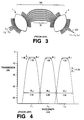
- the WDM of FIG. 3 corresponds to the one disclosed in U. S. Patent 5,412,744 (the '744 patent).
- the transmission characteristics of three particular channels are illustrated in FIG. 4 where it is noted that the figure-of-merit B 1 /B 2 for this design is equal to 0.36, which represents a substantial improvement. An even greater improvement is shown in US-A-5 706 577 .
- a wave division multiplexer includes a pair or star couplers that are interconnected by a grating that comprises an array of unequal-length waveguides. By selecting the lengths of the grating's waveguides in a novel manner, the passbands of the WDM are made flatter than conventional Gaussian passbands associated with such devices.
- the waveguides are grouped according to length ( l i ) into at least two groups. The first group has lengths that differ from each other by multiples of a first constant length ( ⁇ l 1 ); whereas the second group of waveguides has lengths that differ from each other by multiples of a second constant length ( ⁇ l 2 ); where ⁇ l 1 ⁇ ⁇ l 2 .
- the two groups of waveguides are interleaved.
- l o is the length of a central waveguide in the grating.
- the group 1 waveguides are positioned on one side of the central waveguide while the group 2 waveguides are positioned on the other side of the central waveguide.
- FIG. 1 discloses a prior-art optical multiplexer/demultiplexer 100, which is described in U. S. Patent 5,136,671.
- optical multiplexer/demultiplexer 100 comprises a pair of star couplers 1, 2 that are interconnected by a grating 30 that is made from a number of unequal-length optical waveguides.
- An N x N star coupler couples the lightwave from any input to all of the outputs without wavelength selectivity. It is widely used as a basic cross-connect element in passive optical networks. Ideally, the optical power from any input splits evenly into all the outputs without power loss, so that each output receives 1/N of the input power.
- Star coupler 1 comprises a dielectric slab 10 which comprises a free-space region having two curved, preferably circular, boundaries 10 a and 10 b . Power transfer in star coupler 1, between input array 15 and output array 16, is accomplished through radiation in the dielectric slab 10.
- FIG. 1 shows an array 15 of input waveguides radially directed from input ports toward a focal point F2. Each of the input waveguides is connected to the free-space region 10 in a substantially uniform fashion along boundary 10 a .
- An array 16 of output waveguides is radially directed toward a focal point F1. Each of the waveguides in the array 16 is also connected to the free-space region 10 in a substantially uniform fashion along boundary 10 b .
- each waveguide in the grating 30 differs from the lengths of all the other waveguides in the grating so that predetermined and different phase shifts are applied to optical signals propagating through the waveguides of the grating from the star coupler 1 because of the different path lengths over which the signals in the grating must travel to reach the output of the grating. Accordingly, the optical signals emanating from each of the waveguides of grating 30 have different phases, which are functions of the lengths of the waveguides.
- the waveguides of grating 30 are connected to another array 25 of waveguides which are radially directed toward a focal point F4.
- the array 25 connects the output of the grating 30 to the input of the second star coupler 2.
- star coupler 2 comprises a slab of dielectric material 20 forming a free-space region having two curved, preferably circular, boundaries 20 a and 20 b .
- the array 25 of input waveguides is connected to the free-space region in a substantially uniform distribution along boundary 20 a .
- An array 26 of output waveguides are radially directed from output ports toward a focal point F3.
- the waveguides of array 26 are also connected to the free-space region 20 in a substantially uniform distribution along the boundary 20 b .
- Device 100 combines individual channels, which are illustratively present on each of three waveguides of array 15, onto a single waveguide in the array 26. In this direction of transmission, multiplexing is achieved.
- the center frequencies of these three channels are designated ⁇ 1 , ⁇ 2 , and ⁇ 3 in FIG. 1.
- ⁇ 1 , ⁇ 2 , ⁇ 3 and the various path lengths of grating 30 must be carefully selected.
- device 100 is bi-directional, demultiplexing occurs in the opposite direction. For example, if array 26 is now used as the input array, then device 100 will operate to route channels, which are all present on a single waveguide 201 of array 26, onto different waveguides of array 15 according to their wavelengths. The transmission loss of each channel (in either direction) is shown in FIG. 2.
- FIG. 2 discloses the transmission characteristic for multiplexer/demultiplexer 100 (shown in FIG. 1) for three adjacent channels.
- B 1 is the bandwidth between the wavelengths where the channel gain has dropped by 1 dB from its maximum level (illustratively 0.45 nm)
- B 2 is the bandwidth between the wavelengths where the channel gain has dropped by an additional 30 dB (illustratively, 2.65 nm).
- Each channel shown in FIG. 2 has a Gaussian shape; accordingly, multiplexer/demultiplexer 100 has a figure-of-merit (B 1 /B 2 ) equal to 0.17.
- FIG. 3 discloses another prior-art optical multiplexer/demultiplexer 300 of the type shown and described in the '744 patent. It is similar to optical multiplexer/demultiplexer 100 shown in FIG. 1, except that it includes a Y-branch splitter 320 connected to the ends of a pair of adjacent waveguides at the output of star coupler 2.
- each channel has an intrinsic loss of about 5 dB. And while such a loss is undesirable, the associated figure of merit (B 1 /B 2 ) is now equal to 0.36 as indicated in FIG. 4, and this represents a substantial improvement over the design shown in FIG. 1.
- the spacing between adjacent channels is illustratively B 2 , which is about 2.90 nm for the design shown in FIG. 3.
- the present invention relates to planar waveguides whose construction is generally understood and described in numerous articles and patents.
- the most advanced and technically developed planar waveguides are doped-silica waveguides fabricated with silicon optical bench (SiOB) technology.
- SiOB silicon optical bench
- a doped-silica waveguide is usually preferred because it has a number of attractive properties including low cost, low insertion loss, low birefringence, stability, and compatibility for coupling to fiber.
- the processing steps are compatible with those in silicon integrated circuit (IC) technology, which are geared for mass production and are readily known.
- IC integrated circuit
- a doped-silica waveguide is formed by initially depositing a base or lower cladding layer of low index silica on a silicon or silica substrate.
- the core layer is subsequently patterned or sculpted into structures required by the optical circuits using photo-lithographic techniques similar to those used in integrated circuit fabrication.
- a top cladding layer is deposited to cover the patterned waveguide core.
- flat passbands can be achieved by judiciously selecting the lengths of the waveguides within the grating between star couplers of a WDM.
- an ordered array of unequal-length waveguides 30 interconnect a pair of star couplers 1, 2.
- the waveguides of the present invention are grouped according to length (l i ) into at least two groups.
- the first group has lengths that differ from each other by multiples of a first predetermined length ( ⁇ l 1 ); whereas the second group of waveguides has lengths that differ from each other by multiples of a second predetermined length ( ⁇ l 2 ); where ⁇ l 1 ⁇ ⁇ l 2 .
- FIG. 5 discloses an optical multiplexer 500, according to the invention, having a plurality of unequal-length waveguides 50 that interconnect a pair of star couplers 1, 2.
- the optical multiplexer 500 is generally similar to the optical multiplexer shown in FIG. 1 and described in U.S. Patent 5,136,671 which is hereby incorporated by reference for its detailed disclosure of such WDMs.
- waveguides 50 of the present invention have a different length arrangement than the waveguides 30 shown in prior-art FIG. 1.
- the first group of waveguides 501 are interleaved with a second group of waveguides 502.
- waveguide 51 is a central waveguide in the grating 50 that has a length of (l o ), but it is not necessarily associated with group 501 or group 502.
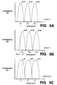
- the first group of waveguides 501 generates a transmission characteristic such as shown in FIG. 9A
- the second group of waveguides 502 generates a transmission characteristic such as shown in FIG. 9B. Note that the transmission characteristics of FIG.
- FIG. 9A and 9B are identical, but are shifted in wavelength by an amount ⁇ 0 which is discussed below.
- an overall transmission characteristic such as shown in FIG. 9C.
- an optical multiplexer having flat passbands is constructed without the disadvantages associated with Y-branch splitters.
- FIG. 6 represents a preferred embodiment of the invention because the group 1 and group 2 waveguides are symmetrically positioned across the entire grating 50. As shown, they are interleaved, one at a time, across the entire grating.
- Another technique (not shown) for symmetrically positioning the waveguides across the entire grating is to interleave the group 1 and group 2 waveguides, two at a time. Symmetrical positioning of these waveguides generates substantially identical transmission characteristics for each the groups as indicated in FIG. 9A and 9B. Nevertheless, the benefits of the present invention also accrue to non-symmetrical arrangements as discussed below.
- FIG. 7 illustrates another embodiment of an optical multiplexer 500 having flat passbands, according to the invention, in which the waveguides of the first group 501 are clustered together in one array, and the waveguides of the second group 502 are clustered together in another array.
- the groups are positioned on opposite sides of the central waveguide 51 of the grating 50, which causes the transmission characteristic of each group to be slightly different from the other. Nevertheless, the advantages of the present invention still accrue to this embodiment.
- optical multiplexer Specific parameters for the design of an optical multiplexer are based on the number of channels to be multiplexed, the channel wavelengths, the desired bandwidth of the various channels, and the properties of the materials used in the construction of the optical multiplexer. Reference is now made to FIG. 8 for a discussion of these considerations.
- FIG. 8 shows the overall transmission characteristic of a waveguide grating router (WGR), which is frequently used as an M x N WDM as in the present invention.
- WGR waveguide grating router
- the principle of the WGR can be described as follows: the lightwave from an input waveguide couples into the grated waveguides by the input star coupler. If there were no differential phase shift in the grating region, the lightwave propagation in the output star would appear as if it were the reciprocal propagation in the input star. The input waveguide would thus be imaged at the interface between the output slab and the output waveguides. The imaged input waveguide would be butt-coupled to one of the output waveguides.
- the linear length difference in the waveguide grating results in a wavelength-dependent tilt of the wave front of the lightwave in the grating waveguides, and thus shifts the input waveguide image to a wavelength-dependent position. As the wavelength changes, the input waveguide image sweeps across and couples light into different output waveguides.
- Silica-based optical integrated circuits at pages 274-276.
- the periodic nature of optical gratings is noted, wherein the period of the grating is known as its "free spectral range" (FSR).
- FSR free spectral range
- each channel has 100 GHz bandwidth (i.e., 0.8 nm)
- the required FSR would be 6.4 nm (i.e., 8 x 0.8 nm).
- FIG. 9A-9C visually illustrates the additive combination of Gaussian channels 90-A1, 90-A2 and 90-A3 with Gaussian channels 90-B1, 90-B2 and 90-B3, respectively, to form channels 80-1, 80-2 and 80-3, which have flatter passbands.
- Gaussian channel 90-A1 represents the transmission characteristic associated with the group 1 waveguides in the preferred embodiment of FIG. 6, and is centered at wavelength ⁇ A1 .
- Gaussian channel 90-B1 is the transmission characteristic associated with the group 2 waveguides in the preferred embodiment of FIG. 6, and is centered at wavelength ⁇ B1 . It has been determined that a suitably flat passband 80-1 can be achieved, as shown in FIG.
Landscapes
- Physics & Mathematics (AREA)
- Engineering & Computer Science (AREA)
- Microelectronics & Electronic Packaging (AREA)
- General Physics & Mathematics (AREA)
- Optics & Photonics (AREA)
- Optical Integrated Circuits (AREA)
Applications Claiming Priority (2)
| Application Number | Priority Date | Filing Date | Title |
|---|---|---|---|
| US84102197A | 1997-04-29 | 1997-04-29 | |
| US841021 | 1997-04-29 |
Publications (2)
| Publication Number | Publication Date |
|---|---|
| EP0875776A2 true EP0875776A2 (de) | 1998-11-04 |
| EP0875776A3 EP0875776A3 (de) | 2000-08-16 |
Family
ID=25283819
Family Applications (1)
| Application Number | Title | Priority Date | Filing Date |
|---|---|---|---|
| EP98303056A Withdrawn EP0875776A3 (de) | 1997-04-29 | 1998-04-21 | Optischer Multiplexer mit flacher Durchlasscharakteristik |
Country Status (2)
| Country | Link |
|---|---|
| EP (1) | EP0875776A3 (de) |
| JP (1) | JPH10307224A (de) |
Cited By (4)
| Publication number | Priority date | Publication date | Assignee | Title |
|---|---|---|---|---|
| US9432121B2 (en) | 2014-06-05 | 2016-08-30 | Xilinx, Inc. | Optical communication circuits |
| US9520949B2 (en) | 2014-06-05 | 2016-12-13 | Xilinx, Inc. | Optical communication circuits |
| US10147666B1 (en) | 2014-07-31 | 2018-12-04 | Xilinx, Inc. | Lateral cooling for multi-chip packages |
| CN113867085A (zh) * | 2020-06-30 | 2021-12-31 | 华为技术有限公司 | 激光芯片和激光投影显示设备 |
Citations (5)
| Publication number | Priority date | Publication date | Assignee | Title |
|---|---|---|---|---|
| US5136671A (en) * | 1991-08-21 | 1992-08-04 | At&T Bell Laboratories | Optical switch, multiplexer, and demultiplexer |
| EP0629885A1 (de) * | 1993-06-17 | 1994-12-21 | AT&T Corp. | Optischer Wellenleiter mit Bandpass-Filter |
| US5412744A (en) * | 1994-05-02 | 1995-05-02 | At&T Corp. | Frequency routing device having a wide and substantially flat passband |
| US5467418A (en) * | 1994-09-02 | 1995-11-14 | At&T Ipm Corp. | Frequency routing device having a spatially filtered optical grating for providing an increased passband width |
| EP0831346A1 (de) * | 1996-09-24 | 1998-03-25 | France Telecom | Wellenleitergitter-Spektrograph als Multiplexer-Komponente |
-
1998
- 1998-04-21 EP EP98303056A patent/EP0875776A3/de not_active Withdrawn
- 1998-04-30 JP JP12047798A patent/JPH10307224A/ja active Pending
Patent Citations (5)
| Publication number | Priority date | Publication date | Assignee | Title |
|---|---|---|---|---|
| US5136671A (en) * | 1991-08-21 | 1992-08-04 | At&T Bell Laboratories | Optical switch, multiplexer, and demultiplexer |
| EP0629885A1 (de) * | 1993-06-17 | 1994-12-21 | AT&T Corp. | Optischer Wellenleiter mit Bandpass-Filter |
| US5412744A (en) * | 1994-05-02 | 1995-05-02 | At&T Corp. | Frequency routing device having a wide and substantially flat passband |
| US5467418A (en) * | 1994-09-02 | 1995-11-14 | At&T Ipm Corp. | Frequency routing device having a spatially filtered optical grating for providing an increased passband width |
| EP0831346A1 (de) * | 1996-09-24 | 1998-03-25 | France Telecom | Wellenleitergitter-Spektrograph als Multiplexer-Komponente |
Non-Patent Citations (1)
| Title |
|---|
| LI Y P ET AL: "SILICA-BASED OPTICAL INTEGRATED CIRCUITS" IEE PROCEEDINGS: OPTOELECTRONICS,GB,INSTITUTION OF ELECTRICAL ENGINEERS, STEVENAGE, vol. 143, no. 5, 1 October 1996 (1996-10-01), pages 263-280, XP000680739 ISSN: 1350-2433 * |
Cited By (8)
| Publication number | Priority date | Publication date | Assignee | Title |
|---|---|---|---|---|
| US9432121B2 (en) | 2014-06-05 | 2016-08-30 | Xilinx, Inc. | Optical communication circuits |
| US9520949B2 (en) | 2014-06-05 | 2016-12-13 | Xilinx, Inc. | Optical communication circuits |
| US10014949B1 (en) | 2014-06-05 | 2018-07-03 | Xilinx, Inc. | Optical communication circuits |
| US10476598B1 (en) | 2014-06-05 | 2019-11-12 | Xilinx, Inc. | Optical communication circuits |
| US11018772B1 (en) | 2014-06-05 | 2021-05-25 | Xilinx, Inc. | Optical communication circuits |
| US10147666B1 (en) | 2014-07-31 | 2018-12-04 | Xilinx, Inc. | Lateral cooling for multi-chip packages |
| CN113867085A (zh) * | 2020-06-30 | 2021-12-31 | 华为技术有限公司 | 激光芯片和激光投影显示设备 |
| CN113867085B (zh) * | 2020-06-30 | 2022-12-06 | 华为技术有限公司 | 激光芯片和激光投影显示设备 |
Also Published As
| Publication number | Publication date |
|---|---|
| JPH10307224A (ja) | 1998-11-17 |
| EP0875776A3 (de) | 2000-08-16 |
Similar Documents
| Publication | Publication Date | Title |
|---|---|---|
| EP0911659B1 (de) | Optischer Einfüge/Abzweig-Multiplexer mit komplementären Stufen | |
| US6351581B1 (en) | Optical add-drop multiplexer having an interferometer structure | |
| EP0856755B1 (de) | Verlustarmer Lichtwellenleiterkoppler | |
| US5706377A (en) | Wavelength routing device having wide and flat passbands | |
| EP0922973B1 (de) | Temperaturkompensierter optischer Multiplexer/Demultiplexer | |
| EP1226461B1 (de) | Phasar mit flacher durchlasskurve | |
| US6141467A (en) | Wavelength-division-multiplexing programmable add/drop using interleave-chirped waveguide grating router | |
| US6181849B1 (en) | Interleaved wavelengths multi/demultiplexer with multiple-input-ports and multiple-output-ports for wavelength add/drop WDM systems | |
| US9780903B2 (en) | Optical wavelength demultiplexer having optical interference filters connected in cascade | |
| EP1225461B1 (de) | Auf einem einzigen Stufengitter basierender bidirektionaler Wellenlängenmultiplexer/-demultiplexer | |
| EP1148358B1 (de) | Ein optischer Multiplexer/Demultiplexer nach der Art des Wellenleitergitters | |
| US6266460B1 (en) | Large-channel-count programmable wavelength add-drop | |
| US6496616B2 (en) | Miniature monolithic optical demultiplexer | |
| US20020176660A1 (en) | Optical wavelength multiplexer/demultiplexer and use method thereof | |
| EP0936483A2 (de) | Optischer Verzweiger mit koherenten Verbindungspfaden | |
| Doerr et al. | Compact and low-loss manner of waveguide grating router passband flattening and demonstration in a 64-channel blocker/multiplexer | |
| EP0875776A2 (de) | Optischer Multiplexer mit flacher Durchlasscharakteristik | |
| US20020081062A1 (en) | Optical grating based multi-input demultiplexer for multiple sets of interleaved wavelength channels | |
| US6728447B2 (en) | Optical multiplexer/demultiplexer | |
| US20050047722A1 (en) | Wideband arrayed waveguide grating | |
| Okamoto et al. | Eight-channel flat spectral response arrayed-waveguide multiplexer with asymmetrical Mach-Zehnder filters | |
| Elrofai | Review paper of array waveguide grating (AWG) | |
| US6658181B2 (en) | Polarization interleaver | |
| EP0962793A1 (de) | Optische Weichenanordnung mit Wellenleitergitter | |
| JP2002341158A (ja) | アレイ導波路格子型光波長合分波器 |
Legal Events
| Date | Code | Title | Description |
|---|---|---|---|
| PUAI | Public reference made under article 153(3) epc to a published international application that has entered the european phase |
Free format text: ORIGINAL CODE: 0009012 |
|
| AK | Designated contracting states |
Kind code of ref document: A2 Designated state(s): AT BE CH CY DE DK ES FI FR GB GR IE IT LI LU MC NL PT SE |
|
| AX | Request for extension of the european patent |
Free format text: AL;LT;LV;MK;RO;SI |
|
| PUAL | Search report despatched |
Free format text: ORIGINAL CODE: 0009013 |
|
| STAA | Information on the status of an ep patent application or granted ep patent |
Free format text: STATUS: THE APPLICATION HAS BEEN WITHDRAWN |
|
| AK | Designated contracting states |
Kind code of ref document: A3 Designated state(s): AT BE CH CY DE DK ES FI FR GB GR IE IT LI LU MC NL PT SE |
|
| AX | Request for extension of the european patent |
Free format text: AL;LT;LV;MK;RO;SI |
|
| 18W | Application withdrawn |
Withdrawal date: 20000613 |