EP0875767A2 - Device and procedure for testing naked circuit boards - Google Patents
Device and procedure for testing naked circuit boards Download PDFInfo
- Publication number
- EP0875767A2 EP0875767A2 EP97118639A EP97118639A EP0875767A2 EP 0875767 A2 EP0875767 A2 EP 0875767A2 EP 97118639 A EP97118639 A EP 97118639A EP 97118639 A EP97118639 A EP 97118639A EP 0875767 A2 EP0875767 A2 EP 0875767A2
- Authority
- EP
- European Patent Office
- Prior art keywords
- basic grid
- circuit board
- contact points
- test
- test device
- Prior art date
- Legal status (The legal status is an assumption and is not a legal conclusion. Google has not performed a legal analysis and makes no representation as to the accuracy of the status listed.)
- Granted
Links
Images


Classifications
-
- G—PHYSICS
- G01—MEASURING; TESTING
- G01R—MEASURING ELECTRIC VARIABLES; MEASURING MAGNETIC VARIABLES
- G01R1/00—Details of instruments or arrangements of the types included in groups G01R5/00 - G01R13/00 and G01R31/00
- G01R1/02—General constructional details
- G01R1/06—Measuring leads; Measuring probes
- G01R1/067—Measuring probes
- G01R1/073—Multiple probes
- G01R1/07307—Multiple probes with individual probe elements, e.g. needles, cantilever beams or bump contacts, fixed in relation to each other, e.g. bed of nails fixture or probe card
- G01R1/07314—Multiple probes with individual probe elements, e.g. needles, cantilever beams or bump contacts, fixed in relation to each other, e.g. bed of nails fixture or probe card the body of the probe being perpendicular to test object, e.g. bed of nails or probe with bump contacts on a rigid support
- G01R1/07328—Multiple probes with individual probe elements, e.g. needles, cantilever beams or bump contacts, fixed in relation to each other, e.g. bed of nails fixture or probe card the body of the probe being perpendicular to test object, e.g. bed of nails or probe with bump contacts on a rigid support for testing printed circuit boards
-
- G—PHYSICS
- G01—MEASURING; TESTING
- G01R—MEASURING ELECTRIC VARIABLES; MEASURING MAGNETIC VARIABLES
- G01R31/00—Arrangements for testing electric properties; Arrangements for locating electric faults; Arrangements for electrical testing characterised by what is being tested not provided for elsewhere
- G01R31/28—Testing of electronic circuits, e.g. by signal tracer
- G01R31/2801—Testing of printed circuits, backplanes, motherboards, hybrid circuits or carriers for multichip packages [MCP]
- G01R31/2805—Bare printed circuit boards
Definitions
- the invention relates to an apparatus and a method for Checking bare PCBs.
- Printed circuit boards have a large number of networks, their Density on the printed circuit boards increases with the continuously progressing Miniaturization of electronic components increasingly increased.
- Known devices for testing printed circuit boards can are basically divided into two groups. To the first The group includes the so-called parallel testers, which are test devices with adapter, with which all PCB test points a circuit board contacted simultaneously by means of the adapter will. The second group includes the so-called finger testers. These are devices with two or more test fingers scan the individual PCB test points sequentially.
- Test devices with adapters go, for example, from DE 42 37 591 A1, DE 44 06 538 A1, DE 43 23 276 A1, EP 215 146 B1 and DE 38 38 413 A1.
- Such adapters basically serve the uneven Configuration of the circuit board test points of the circuit board to be tested to the specified basic grid of the electrical test device adapt.
- the circuit board test points are no longer in a uniform Arranged grid, which is why the connection between the Contact grid and the circuit board test points Contact needles in the adapter with an inclination or deflection are arranged or a so-called translator is provided which is the even contact grid in the uneven Configuration of the PCB test points "translated".
- the individual Networks for interruptions in the networks (“interruption test") and on electrical connections to other networks (“short circuit test”) tested.
- the short circuit test can both the detection of low-resistance as well as high-resistance connections.
- the invention has for its object a simply trained Device for testing bare printed circuit boards create with the PCB with a high PCB test point density and / or very small distances between the PCB test points can be tested.
- the task is performed by a device with the features of Claim 1 solved.
- the test device has evaluation electronics, which is electrically connected to a basic grid.
- On the basic grid stores an adapter.
- One is to be tested on the adapter Printed circuit board, the adapter an electrical Contact between the circuit board test points on the circuit board and one contact point and one respectively Produces the pad field of the basic grid.
- One can be in the adapter Translatorboard be used, with which the electrical Connections from a contact point to a remote one PCB test point of the PCB redirected can be.
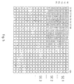
- the device according to the invention has a basic grid 1 several contact points 2 on a basic grid 3 are formed. There are at least two contact points 2 of the Basic grid 1 in the basic grid plate 3 is electrically connected.
- the basic grid plate 3 is preferably made of a laminated Printed circuit board.
- the embodiment shown in Fig. 2 has an upper and a lower boundary layer 4, 5 and thirteen liners 6.
- the vias 7 are in the Usually as holes with a conductive, metallized coating educated.
- the plated-through holes 7 are, for example, in arranged in a regular square grid, the Center distance a between two plated-through holes 7, for example 500 ⁇ m is. In the case of ceramic basic grid plates 3, the center distance can be a can be reduced to 100 ⁇ m. They are too other types of regular screening are possible, e.g. a rectangular or hexagonal grid or also a grid, at which the vias 7 of adjacent rows to each other are staggered.
- the vias 7 and the corresponding contact points 2 are thus in rows (R1, R2, ...) and columns (S1, S2, ...) arranged (Fig. 1). Between two rows of vias 7 are each conductor tracks 10 embedded in the basic grid plate 3, the following as Scan channels are called.
- the one shown in FIG. 1 Embodiment are between two rows of vias 7 each twelve and in the one shown in FIG. 2 Embodiment provided twenty-four scan channels 10 each, each in pairs in an intermediate layer between two intermediate layers 6 are arranged.
- the twelve pairs each arranged adjacent to a row of vias 7 Scan channels 10 are assigned to this row, i.e. each Vias 7 and thus each contact point 2 a certain Row electrically with one of the assigned to this row Scan channels 10 is connected via a stub 11.
- Fig. 2 36 channels are designated K1 to K36, in Fig. 1 in the contact points 2 of the first three rows the numbers of the channels are entered with which they are electrical are connected. 1, every twelfth are in a row Contact point 2 is electrically connected to the same scan channel 10 is. One therefore speaks of a repetition sequence of twelve. In other words, every twelfth contact point 2 of a row electrically connected via a scan channel 10 is. There are thus a number of contact points 2 each detected with a scan channel 10. This simplifies the conductor track structure in the basic grid plate 3 essentially, so that the vias 7 with a much smaller distance than with conventional basic grid plates can, making the grid density of the contact points essential can be increased.
- the scan channels 10 are on the edges of the basic grid plate 3 electrical connectors like. e.g. Connector connected to which the scan or evaluation electronics are connected can.
- Connector connected to which the scan or evaluation electronics are connected can.
- Despite a large number of contact points 2 on the basic grid 1 is the number of test connections of the evaluation electronics relatively small, because only for each scan channel a test connection must be provided.
- With known test devices is a separate test connection for each contact point provided for evaluation electronics. Compared to this known The electronic evaluation equipment is considerably reduced, namely to the extent that the contact points combined on the scan channels and the test connections reduced will.
- any suitable removable and permanent electrical connection at the interface between the basic grid plate 3 and the evaluation electronics are provided will.
- E.g. can connect the test connections to the scan channels be soldered on.
- Such an inseparable electrical connection is particularly suitable when the evaluation electronics are in the Basic grid plate 3 integrated or below the basic grid plate 3 is attached to this.
- the mechanical structure of the device according to the invention is also very easy because the electrical connections are on the side the basic grid plate 3 are arranged so that the electronics be arranged spatially separate from the basic grid plate 3 can. So you can directly under the basic grid plate Printing elements, e.g. a pressure plate to be arranged with which the basic grid plate 3 and an adapter and / or a Translator can be printed against the circuit board to be tested.
- Printing elements e.g. a pressure plate to be arranged with which the basic grid plate 3 and an adapter and / or a Translator can be printed against the circuit board to be tested.
- circuit board test point nests in which the circuit board test points in high density are arranged close together, whereas the rest Printed circuit board test points with a larger distance on the Printed circuit board are arranged. Only in the area of the circuit board test point nests will be the vast number of contact points 2 of the basic grid 1 contacted, whereas most of the others Contact points are not used. Therefore, through a clever arrangement of the circuit board on the test device such undesirable electrical connections or short circuits be avoided.
- 3a to 3c such are schematically simplified Arrangements are shown, with the representation only on the contour of the circuit board 12 to be tested, its circuit board test point nests 13 and the course of the scan channels 10 limited.
- 3a is the rectangular circuit board 12 with their side edges 15 arranged obliquely to the scan channels 10.
- the circuit board test point nests 13 are on the circuit board 12 usually along parallel to the side edges 15 running rows arranged so that by the inclination can prevent multiple board test point nests are arranged over the same scan channels 10.
- the likelihood that a Scan channel with several circuit board test points of the to be tested Printed circuit board 12 is contacted.
- a basic grid plate 3 is shown, the scan channels 10 not across the entire width or length of the Basic grid plate 3 extend, but in two from each other separate areas 16, 17 along one diagonally on the basic grid plate 3 extending dividing line 18 are divided.
- the two Areas 16, 17 are completely electrically decoupled from one another, so that there is no electrical connection crossing the dividing line 18 can occur via the scan channels 10.
- the basic grid plate 3 is also mechanically in the divided into two areas 16, 17.
- the mechanical dividing line does not have to be between the electrically decoupled regions 16, 17 run, but can also between any two scan channels 10 may be arranged.
- the basic grid plate can also be decoupled from one another Areas 19, 20, 21, 22 electrically and / or mechanically be divided (Fig. 3c), the dividing lines 23, 24 preferably are arranged diagonally on the basic grid plate 3.
- the problem of unwanted electrical connections can also be confronted during the construction of the adapters arranged between the basic grid and the circuit board to be tested are, whereby the adapter is arranged on the basic grid and the assignment of the contact points of the basic grid to the networks of the circuit board to be tested is chosen so that unwanted electrical connections do not occur. This is often possible because there are usually many contact points in the basic grid not be used and only the contact points in the Area of the circuit board test point nests can be used intensively.
- Adapters usually have needles that are electrical Contact between the contact points 2 and the circuit board test points the circuit board to be tested or one in between produce arranged translator. By a slight inclination the needles can connect from a circuit board test point the circuit board to a not immediately perpendicular Contact point 2 located below the circuit board test point of the basic grid 1 are produced. Since on the invention Basic grid 1 the contact points 2 very close to each other can be arranged easily with a single Needle a range of e.g. 16 contact points 2 addressed wedren. This allows a contact point 2 from a Group of contact points arranged close to one another 2 can be selected, which also creates a corresponding scan channel 10 is selected. Thus, by the design of the Adapters undesirable electrical connections or short circuits be specifically excluded.
- test devices are usually the Printed circuit boards with their longitudinal direction in the transport direction automated test device aligned.
- a translator board 30 can be integrated in a so-called translator adapter 31, the consists of the translator board 30 and a pin translator adapter 32.
- the pin translator adapter 32 consists of two layers 33, 34 formed, each with vertical bores 35, 36 in same drilling patterns are penetrated so that the holes 35, 36th aligned in pairs to each other. In the lower layer 33 is in the Bores 35 each have a pin-shaped contact spring element 37 arranged.
- a pin 38 is arranged which extends through a bore 36 extends and on the pin translator adapter 32 with its upper end region protrudes.
- the pins 38 are on the contact spring elements 37 vertically yielding.
- translator adapter 31 can also an adapter with oblique smooth needles, bending needles or electrically conductive rubber knobs or another suitable have electrical connecting means.
- the translator board 30 is below the pin translator adapter 32 arranged. It is made of a printed circuit board 39 with it conductor tracks extending from its top to its bottom 40 trained. At the end points of the conductor tracks 40 on the The top and bottom of the translator board is one Contact surface 41o, 41u formed. The contact surfaces 41u the underside of the translator board 30 are over one in itself known full grid adapter with the contact points 2 of the basic grid 1 connected.
- the upper contact surfaces are 41o by a point and the lower contact surfaces 41u by a Ring shown.
- FIG. 5 is another embodiment of an inventive Basic grid shown.
- This basic grid is in 20 horizontal rows (R1 - R20) and 24 vertical columns (S1 - S24) divided. The number of rows and columns is in an actual application will be far larger.
- Four neighboring Rows (R1 - R4; R5 - R8; R9 - R12; etc.) form each a segment (SE1, SE2, SE3, etc.).
- SE1, SE2, SE3, etc.) form each a segment (SE1, SE2, SE3, etc.).
- SE1, SE2, SE3, etc. In the segments is Every fourth contact point in a row with a scan channel connected.
- the segments there are contact points 2 of the individual Rows connected to the same scan channel, the ones with a scan channel connected contact points of two neighboring Rows preferably arranged diagonally on the basic grid plate are.
- Fig. 5 are Four scan channels are provided for each segment.
- the scan channels have electrical ones Connections to contact points 2 from several rows, where the contact points 2 of neighboring ones connected with a scan channel Rows or columns preferably offset from one another are arranged. Since the scan channels with contact points from several Rows are connected, the number of scan channels continues reduced.
- the scan channels 10 between the individual layers 6 in the basic grid plate 3 can in the top view of the basic grid plate 3 arranged in different directions and in particular be perpendicular to each other, creating a local Selectivity is achieved.
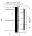
- This device has a solid table 55 with a Table top 56 on.
- the table top 56 is insulated and on it stores a basic grid plate 3 according to the invention on the basic grid plate 3 is an adapter 58 with needles 59, in particular Rigid needle, arranged.
- the needles 59 can be used to select one certain scan channel in the manner described above be slanted.
- the one to be tested is mounted on the adapter 58 Printed circuit board 51, which by means of a stamp 60 against the Adapter is printed.
- the basic grid plate 3 has one over the table plate 56 protruding connection area 62 in which the scan channels (not shown) are extended.
- connection area 62 are units 64 of the evaluation electronics on the underside arranged and electrically with the scan channels by means of contact pins 65 or the like connected.
- These contact pins 65 extend vertically through the basic grid plate 3 and stand at the top.
- Is above the connection area 62 an electrically conductive plate 66 parallel to the basic grid plate 3 arranged, and vertically displaceable in the double arrow direction 67 stored. Plate 66 is grounded.
- connection area 62 forms together with the electrical grounded plate 66 a grounding device that allows it and after a measuring process, which in the circuit board 51 and / or in the measuring device (basic grid plate, adapter, evaluation electronics, etc.) electrical potentials by contacting the plate 66 with the contact pins projecting upwards 65.
- This can be very fast defined electrical conditions are created and the Pauses between the individual measuring processes, which are used to derive the electrical potentials in conventional test devices are significantly reduced.
- contact pins 65 above can also be used elsewhere exposed contact points are provided on the basic grid plate be with the scan channels and thus with the evaluation electronics and electrically connected to the circuit board to be tested are. By touching the contact points with an earthed conductor the circuit board to be tested and the evaluation electronics grounded.
- a base or can of course the like are provided; it just has to be a stable one Support for the basic grid plate 3 can be created.
Landscapes
- Physics & Mathematics (AREA)
- General Physics & Mathematics (AREA)
- Engineering & Computer Science (AREA)
- Computer Hardware Design (AREA)
- Microelectronics & Electronic Packaging (AREA)
- General Engineering & Computer Science (AREA)
- Tests Of Electronic Circuits (AREA)
- Testing Of Short-Circuits, Discontinuities, Leakage, Or Incorrect Line Connections (AREA)
Abstract
Description
Die Erfindung betrifft eine Vorrichtung und ein Verfahren zum Prüfen von unbestückten Leiterplatten.The invention relates to an apparatus and a method for Checking bare PCBs.
Leiterplatten weisen eine Vielzahl von Netzen auf, wobei deren Dichte auf den Leiterplatten sich mit der kontinuierlich fortschreitenden Miniaturisierung der elektronischen Bauelemente zunehmend erhöht.Printed circuit boards have a large number of networks, their Density on the printed circuit boards increases with the continuously progressing Miniaturization of electronic components increasingly increased.
Bekannte Vorrichtungen zum Prüfen von Leiterplatten können grundsätzlich in zwei Gruppen eingeteilt werden. Zur ersten Gruppe gehören die sogenannten Paralleltester, das sind Prüfvorrichtungen mit Adapter, bei welchen alle Leiterplattentestpunkte einer Leiterplatte gleichzeitig mittels des Adapters kontaktiert werden. Die zweite Gruppe umfaßt die sogenannten Fingertester. Das sind Vorrichtungen, die mit zwei oder mehreren Prüffingern die einzelnen Leiterplattentestpunkte sequentiell abtasten.Known devices for testing printed circuit boards can are basically divided into two groups. To the first The group includes the so-called parallel testers, which are test devices with adapter, with which all PCB test points a circuit board contacted simultaneously by means of the adapter will. The second group includes the so-called finger testers. These are devices with two or more test fingers scan the individual PCB test points sequentially.
Prüfvorrichtungen mit Adapter gehen bspw. aus der DE 42 37 591 A1, der DE 44 06 538 A1, der DE 43 23 276 A1, der EP 215 146 B1 und der DE 38 38 413 A1 hervor.Test devices with adapters go, for example, from DE 42 37 591 A1, DE 44 06 538 A1, DE 43 23 276 A1, EP 215 146 B1 and DE 38 38 413 A1.
Derartige Adapter dienen grundsätzlich dazu, die ungleichmäßige Konfiguration der Leiterplattentestpunkte der zu testenden Leiterplatte an das vorgegebene Grundraster der elektrischen Prüfvorrichtung anzupassen. Bei modernen, zu testenden Leiterplatten sind die Leiterplattentestpunkte nicht mehr in einem gleichmäßigen Raster angeordnet, weshalb die die Verbindung zwischen dem Kontaktraster und den Leiterplattentestpunkten herstellenden Kontaktnadeln im Adapter mit einer Schrägstellung bzw. Auslenkung angeordnet sind oder ein sogenannter Translator vorgesehen ist, der das gleichmäßige Kontaktraster in die ungleichmäßige Konfiguration der Leiterplattentestpunkte "übersetzt".Such adapters basically serve the uneven Configuration of the circuit board test points of the circuit board to be tested to the specified basic grid of the electrical test device adapt. For modern circuit boards to be tested the circuit board test points are no longer in a uniform Arranged grid, which is why the connection between the Contact grid and the circuit board test points Contact needles in the adapter with an inclination or deflection are arranged or a so-called translator is provided which is the even contact grid in the uneven Configuration of the PCB test points "translated".
Unabhängig von der Art der Vorrichtung werden die einzelnen Netze auf Unterbrechungen in den Netzen ("Unterbrechungstest") und auf elektrische Verbindungen zu anderen Netzen ("Kurzschlußtest") getestet. Der Kurzschlußtest kann sowohl die Detektion von niederohmigen als auch von hochohmigen Verbindungen umfassen.Regardless of the type of device, the individual Networks for interruptions in the networks ("interruption test") and on electrical connections to other networks ("short circuit test") tested. The short circuit test can both the detection of low-resistance as well as high-resistance connections.
Sowohl für den Unterbrechungstest als auch für den Kurzschlußtest sind unterschiedliche Meßverfahren bekannt. Hierbei wird jedes Netz auf einen Kurzschluß bzw. jeder Zweig eines Netzes auf eine Unterbrechung untersucht, so daß bei modernen Leiterplatten mit einer Vielzahl von Netzen eine entsprechend hohe Anzahl einzelner Meßvorgänge durchgeführt werden muß.Both for the interruption test and for the short circuit test different measuring methods are known. Here will every network for a short circuit or branch of a network examined for an interruption, so that with modern circuit boards a correspondingly high level with a large number of networks Number of individual measurements must be carried out.
Man hat versucht, die einzelnen Meßvorgänge zu optimieren und deren Anzahl zu minimieren, wobei eine Vielzahl unterschiedlicher Verfahren vorgeschlagen und umgesetzt worden sind.Attempts have been made to optimize the individual measuring processes and minimize their number, using a variety of different Procedures have been proposed and implemented.
Ferner sind Vorrichtungen zum Prüfen von bestückten Leiterplatten bekannt (z.B. WO96/27136). Der Test von bestückten Leiterplatten unterscheidet sich grundlegend von dem für unbestückte Leiterplatten, da bei bestückten Leiterplatten ein sogenannter Funktionstest ausgeführt werden kann. Dies bedeutet, daß ein jedes Netz der Leiterplatte in der Regel nur an einer einzigen Stelle kontaktiert wird und ein sich in Abhängigkeit von vorbestimmten Spannungen oder Strömen einstellender Spannungs- oder Stromwert gemessen wird. Dies ist möglich, da bei bestückten Leiterplatten alle Funktionselemente (ICs, Transistoren, Widerstände, Kondensatoren, usw.) vorhanden sind und deren Funktion getestet werden kann. Die Anzahl der Kontaktierungen zwischen der Prüfvorrichtung und der zu prüfenden Leiterplatte ist deshalb beim Test von bestückten Leiterplatten wesentlich geringer als beim Test von unbestückten Leiterplatten. Herkömmliche Vorrichtungen zum Prüfen von bestückten Leiterplatten weisen zur Durchführung der Funktionstest Adapter auf, deren Prüfstifte aufwendig verdrahtet sind. Gegenüber solchen Prüfvorrichtungen sieht die WO 96/27136 ein Adaptersystem mit einer Rasterplatte vor, an welcher mehrere Kontaktflachen miteinander über Testkanäle elektrisch verbunden sind, wobei die Kontaktflachen vermischt verteilt auf der Rasterplatte positioniert sind. Das Rastermaß der Rasterplatte beträgt üblicherweise 1,27 mm. Die Verdrahtung wird somit in die Rasterplatte integriert. Eine solche Vorrichtung ist zum Prüfen von unbestückten Leiterplatten, die mit einer viel höheren Kontaktdichte kontaktiert werden müssen, ungeeignet.There are also devices for testing printed circuit boards known (e.g. WO96 / 27136). The test of printed circuit boards differs fundamentally from that for bare Printed circuit boards, since a so-called Function test can be carried out. This means that a each network of the circuit board usually only on one Body is contacted and a depending on predetermined Voltages or currents adjusting voltage or Current value is measured. This is possible because with assembled PCBs all functional elements (ICs, transistors, resistors, Capacitors, etc.) are present and their function can be tested. The number of contacts between the test device and the circuit board to be tested is therefore when testing printed circuit boards much lower than when testing bare circuit boards. Conventional devices for testing printed circuit boards Carrying out the function test adapter on whose test pins are laboriously wired. Compared to such test fixtures WO 96/27136 sees an adapter system with a grid plate in front of which several contact surfaces with each other via test channels are electrically connected, the contact surfaces being mixed are positioned distributed on the grid plate. The The grid dimension of the grid plate is usually 1.27 mm. The Wiring is thus integrated in the grid plate. A such a device is for testing bare printed circuit boards, which are contacted with a much higher contact density must be unsuitable.
Der Erfindung liegt die Aufgabe zugrunde, eine einfach ausgebildete Vorrichtung zum Prüfen von unbestückten Leiterplatten zu schaffen, mit der Leiterplatten mit einer hohen Leiterplattentestpunktdichte und/oder sehr kleinen Abstanden zwischen den Leiterplattentestpunkten getestet werden können.The invention has for its object a simply trained Device for testing bare printed circuit boards create with the PCB with a high PCB test point density and / or very small distances between the PCB test points can be tested.
Die Aufgabe wird durch eine Vorrichtung mit den Merkmalen des
Anspruchs 1 gelöst.The task is performed by a device with the features of
Vorteilhafte Ausgestaltungen der Erfindung sind in den Unteransprüchen angegeben.Advantageous embodiments of the invention are in the subclaims specified.
Die Erfindung wird beispielhaft anhand der Zeichnungen naher erläutert. Es zeigen:
- Fig. 1
- schematisch vereinfacht ein Grundraster in der Draufsicht,
- Fig. 2
- eine Grundrasterplatte im Querschnitt im Bereich zweier Scankanäle,
- Fig. 3a bis 3c
- jeweils schematisch sehr vereinfacht eine Anordnung einer zu prüfenden Leiterplatte auf einer Grundrasterplatte,
- Fig. 4a
- einen Pintranslatoradapter im Querschnitt,
- Fig. 4b
- schematisch die Leiterbahnen eines Translators in der Draufsicht,
- Fig. 5
- schematisch vereinfacht ein weiteres Grundraster in der Draufsicht,
- Fig. 6
- schematisch eine erfindungsgemäße Prüfvorrichtung im Querschnitt.
- Fig. 1
- schematically simplified a basic grid in plan view,
- Fig. 2
- a basic grid plate in cross-section in the area of two scan channels,
- 3a to 3c
- an arrangement of a circuit board to be tested on a basic grid plate is schematically very simplified,
- Fig. 4a
- a pin translator adapter in cross section,
- Fig. 4b
- schematically the conductor tracks of a translator in top view,
- Fig. 5
- schematically simplified another basic grid in plan view,
- Fig. 6
- schematically a testing device according to the invention in cross section.
Die Prüfvorrichtung weist eine Auswerteelektronik auf, welche elektrisch mit einem Grundraster verbunden ist. Auf dem Grundraster lagert ein Adapter. Auf den Adapter wird eine zu prüfende Leiterplatte aufgelegt, wobei der Adapter einen elektrischen Kontakt zwischen den auf der Leiterplatte befindlichen Leiterplattentestpunkten und jeweils einer Kontaktstelle bzw. einem Padfeld des Grundrasters herstellt. In den Adapter kann ein Translatorboard eingesetzt sein, mit welchem die elektrischen Verbindungen von einer Kontaktstelle zu einem davon entfernt angeordneten Leiterplattentestpunkt der Leiterplatte umgeleitet werden können.The test device has evaluation electronics, which is electrically connected to a basic grid. On the basic grid stores an adapter. One is to be tested on the adapter Printed circuit board, the adapter an electrical Contact between the circuit board test points on the circuit board and one contact point and one respectively Produces the pad field of the basic grid. One can be in the adapter Translatorboard be used, with which the electrical Connections from a contact point to a remote one PCB test point of the PCB redirected can be.
Die erfindungsgemäße Vorrichtung weist ein Grundrasterfeld 1 mit
mehreren Kontaktstellen 2 auf, die auf einer Grundrasterplatte
3 ausgebildet sind. Es sind zumindest zwei Kontaktstellen 2 des
Grundrasterfeldes 1 in der Grundrasterplatte 3 elektrisch verbunden.The device according to the invention has a
Die Grundrasterplatte 3 ist vorzugsweise aus einer laminierten
Leiterplatte ausgebildet. Das in Fig. 2 abgebildete Ausführungsbeispiel
weist eine obere und eine untere Begrenzungslage 4, 5
und dreizehn Zwischenlagen 6 auf.The
Von den Kontaktstellen 2 erstreckt sich senkrecht durch die
oberste Lage 4 und alle Zwischenlagen 6 jeweils eine vertikale
Durchkontaktierung 7. Die Durchkontaktierungen 7 sind in der
Regel als Bohrungen mit einer leitenden, metallisierten Beschichtung
ausgebildet. Die Durchkontaktierungen 7 sind bspw. in
einem regelmäßigen quadratischen Raster angeordnet, wobei der
Mittenabstand a zwischen zwei Durchkontaktierungen 7 bspw. 500
µm beträgt. Bei keramischen Grundrasterplatten 3 kann der Mittenabstand
a bis auf 100 µm verringert werden. Es sind auch
andere Arten einer regelmäßigen Rasterung möglich, wie z.B. ein
rechteckiges oder hexagonales Raster oder auch ein Raster, bei
welchem die Durchkontaktierungen 7 benachbarter Reihen zueinander
versetzt angeordnet sind. Die Durchkontaktierungen 7 und
die entsprechenden Kontaktstellen 2 sind somit in Reihen (R1,
R2, ...) und Spalten (S1, S2, ...) angeordnet (Fig. 1). Zwischen
zwei Reihen von Durchkontaktierungen 7 sind jeweils Leiterbahnen
10 in der Grundrasterplatte 3 eingebettet, die nachfolgend als
Scankanäle bezeichnet werden. Bei dem in den Fig. 1 dargestellten
Ausführungsbeispiel sind zwischen zwei Reihen von Durchkontaktierungen
7 jeweils zwölf und bei dem in Fig. 2 dargestellten
Ausführungsbeispiel jeweils vierundzwanzig Scankanäle 10 vorgesehen,
die jeweils paarweise in einer Zwischenschicht zwischen
zwei Zwischenlagen 6 angeordnet sind. Die jeweils zwölf Paare
benachbart zu einer Reihe von Durchkontaktierungen 7 angeordneten
Scankanäle 10 sind dieser Reihe zugeordnet, d.h., daß jede
Durchkontaktierung 7 und damit jede Kontaktstelle 2 einer bestimmten
Reihe elektrisch mit einem der dieser Reihe zugeordneten
Scankanäle 10 über eine Stichleitung 11 verbunden ist.From the contact points 2 extends vertically through the
In Fig. 2 sind 36 Kanäle mit K1 bis K36 bezeichnet, wobei in
Fig. 1 in die Kontaktstellen 2 der ersten drei Reihen die Nummern
der Kanäle eingetragen sind, mit welchen sie elektrisch
verbunden sind. Gemäß Fig. 1 sind in einer Reihe jede zwölfte
Kontaktstelle 2 mit dem gleichen Scankanal 10 elektrisch verbunden
ist. Man spricht deshalb von einer Wiederholungsfolge von
zwölf. Mit anderen Worten heißt dies, daß jede zwölfte Kontaktstelle
2 einer Reihe über einen Scankanal 10 elektrisch verbunden
ist. Es werden somit eine Anzahl von Kontaktstellen 2 jeweils
mit einem Scankanal 10 erfaßt. Hierdurch vereinfacht sich
die Leiterbahnenstruktur in der Grundrasterplatte 3 wesentlich,
so daß die Durchkontaktierungen 7 mit einem viel geringeren Abstand
als bei herkömmlichen Grundrasterplatten angeordnet werden
können, wodurch die Rasterdichte der Kontaktstellen wesentlich
erhöht werden kann. In Fig. 2 36 channels are designated K1 to K36, in
Fig. 1 in the contact points 2 of the first three rows the numbers
of the channels are entered with which they are electrical
are connected. 1, every twelfth are in a
Die Scankanäle 10 sind an den Rändern der Grundrasterplatte 3 an
elektrische Verbinder wie. z.B. Steckverbinder angeschlossen, an
welche die Scan- bzw. Auswerteelektronik angeschlossen werden
kann. Trotz einer Vielzahl von Kontaktstellen 2 auf dem Grundrasterfeld
1 ist die Anzahl der Testanschlüsse der Auswerteelektronik
relativ gering, da lediglich für einen jeden Scankanal
ein Testanschluß vorgesehen werden muß. Bei bekannten Prüfvorrichtungen
ist für jede Kontaktstelle ein eigener Testanschluß
zur Auswerteelektronik vorgesehen. Gegenüber diesen bekannten
Prüfvorrichtungen vermindert sich die Auswerteelektronik erheblich,
nämlich in exakt dem Maße, mit welchem die Kontaktstellen
an den Scankanälen zusammengefaßt und die Testanschlüsse verringert
werden.The
Anstatt eines Steckverbinders kann jede geeignete losbare und
nicht lösbare elektrische Verbindung an der Schnittstelle zwischen
der Grundrasterplatte 3 und der Auswerteelektronik vorgesehen
werden. Bspw. können die Testanschlüsse an die Scankanäle
angelötet sein. Eine solche unlösbare elektrische Verbindung
ist vor allem dann geeignet, wenn die Auswerteelektronik in die
Grundrasterplatte 3 integriert bzw. unterhalb an die Grundrasterplatte
3 an diese anliegend befestigt wird.Instead of a connector, any suitable removable and
permanent electrical connection at the interface between
the
Der mechanische Aufbau der erfindungsgemäßen Vorrichtung ist
zudem sehr einfach, da die elektrischen Anschlüsse seitlich an
der Grundrasterplatte 3 angeordnet sind, so daß die Elektronik
räumlich getrennt von der Grundrasterplatte 3 angeordnet werden
kann. Somit können unmittelbar unter der Grundrasterplatte
Druckelemente, wie z.B. eine Druckplatte, angeordnet sein, mit
welcher die Grundrasterplatte 3 und ein Adapter und/oder ein
Translator gegen die zu prüfende Leiterplatte gedruckt werden.The mechanical structure of the device according to the invention is
also very easy because the electrical connections are on the side
the
Grundsätzlich ist es möglich, daß durch die elektrische Verbindung der Kontaktstellen einzelne Netze der zu prüfenden Leiterplatte elektrisch verbunden werden, so daß eine für sog. Paralleltester (= Prüvorrichtung mit Adapter) herkömmliche Unterbrechungs- bzw. Kurzschlußmessung nicht möglich wäre. Basically, it is possible that through the electrical connection of the contact points individual networks of the circuit board to be tested be electrically connected so that one for so-called parallel testers (= Test device with adapter) conventional interruption or short-circuit measurement would not be possible.
Es hat sich überraschenderweise gezeigt, daß bei einem Großteil
der zu testenden Leiterplatten dieses Problem nicht auftritt, da
die Leiterplatten sogenannte Leiterplattentestpunktnester aufweisen,
in welchen die Leiterplattentestpunkte in hoher Dichte
eng beieinander liegend angeordnet sind, wohingegen die übrigen
Leiterplattentestpunkte mit größerem Abstand verteilt auf der
Leiterplatte angeordnet sind. Nur im Bereich der Leiterplattentestpunktnester
wird die überwiegende Anzahl von Kontaktstellen
2 des Grundrasters 1 kontaktiert, wohingegen die meisten übrigen
Kontaktstellen nicht benutzt werden. Deshalb können durch eine
geschickte Anordnung der Leiterplatte auf der Prüfvorrichtung
derartige unerwünschten elektrischen Verbindungen bzw. Kurzschlüsse
vermieden werden.Surprisingly, it has been shown that for a large part
of the circuit boards to be tested does not experience this problem because
the circuit boards have so-called circuit board test point nests,
in which the circuit board test points in high density
are arranged close together, whereas the rest
Printed circuit board test points with a larger distance on the
Printed circuit board are arranged. Only in the area of the circuit board test point nests
will be the vast number of
In den Fig. 3a bis 3c sind schematisch vereinfacht derartige
Anordnungen dargestellt, wobei sich die Darstellung lediglich
auf die Kontur der zu testenden Leiterplatte 12, deren Leiterplattentestpunktnester
13 und den Verlauf der Scankanäle 10
beschrankt. Gemaß Fig. 3a ist die rechteckförmige Leiterplatte
12 mit ihren Seitenkanten 15 schräg zu den Scankanälen 10 angeordnet.
Die Leiterplattentestpunktnester 13 sind auf der Leiterplatte
12 üblicherweise entlang parallel zu den Seitenkanten
15 verlaufenden Reihen angeordnet, so daß durch die Schrägstellung
verhindert werden kann, daß mehrere Leiterplattentestpunktnester
über den gleichen Scankanälen 10 angeordnet sind. Hierdurch
wird die Wahrscheinlichkeit deutlich verringert, daß ein
Scankanal mit mehreren Leiterplattentestpunkten der zu testenden
Leiterplatte 12 kontaktiert wird.3a to 3c, such are schematically simplified
Arrangements are shown, with the representation only
on the contour of the
In Fig. 3b ist eine Grundrasterplatte 3 dargestellt, deren Scankanäle
10 sich nicht über die gesamte Breite oder Lange der
Grundrasterplatte 3 erstrecken, sondern in zwei voneinander
getrennte Bereiche 16, 17 längs einer diagonal auf der Grundrasterplatte
3 verlaufenden Trennlinie 18 geteilt sind. Die beiden
Bereiche 16, 17 sind elektrisch voneinander vollkommen entkoppelt,
so daß keine die Trennlinie 18 kreuzende elektrische Verbindung
über die Scankanäle 10 auftreten kann. In Fig. 3b, a
Vorzugsweise ist die Grundrasterplatte 3 auch mechanisch in die
beiden Bereiche 16, 17 aufgeteilt. Die mechanische Trennlinie
muß nicht zwischen den elektrisch entkoppelten Bereichen 16, 17
verlaufen, sondern kann auch zwischen zwei beliebigen Scankanälen
10 angeordnet sein.Preferably, the
Die Grundrasterplatte kann auch in mehrere voneinander entkoppelte
Bereiche 19, 20, 21, 22 elektrisch und/oder mechanisch
aufgeteilt sein (Fig. 3c), wobei die Trennlinien 23, 24 vorzugsweise
diagonal auf der Grundrasterplatte 3 angeordnet sind.The basic grid plate can also be decoupled from one another
Dem Problem der unerwünschten elektrischen Verbindungen kann auch bereits beim Bau der Adapter entgegengetreten werden, die zwischen dem Grundraster und der zu prüfenden Leiterplatte angeordnet sind, wobei der Adapter so auf dem Grundraster angeordnet wird und die Zuordnung der Kontaktstellen des Grundrasters zu den Netzen der zu prüfenden Leiterplatte so gewählt wird, daß unerwünschte elektrische Verbindungen nicht auftreten. Dies ist oftmals möglich, da in der Regel viele Kontaktstellen des Grundrasters nicht benutzt werden und lediglich die Kontaktstellen im Bereich der Leiterplattentestpunktnester intensiv benutzt werden.The problem of unwanted electrical connections can also be confronted during the construction of the adapters arranged between the basic grid and the circuit board to be tested are, whereby the adapter is arranged on the basic grid and the assignment of the contact points of the basic grid to the networks of the circuit board to be tested is chosen so that unwanted electrical connections do not occur. This is often possible because there are usually many contact points in the basic grid not be used and only the contact points in the Area of the circuit board test point nests can be used intensively.
Adapter weisen in der Regel Nadeln auf, die einen elektrischen
Kontakt zwischen den Kontaktstellen 2 und den Leiterplattentestpunkten
der zu prüfenden Leiterplatte bzw. einem dazwischen
angeordneten Translator herstellen. Durch eine geringe Schrägstellung
der Nadeln kann die Verbindung von einem Leiterplattentestpunkt
der Leiterplatte zu einer nicht unmittelbar senkrecht
unter dem Leiterplattentestpunkt angeordneten Kontaktstelle 2
des Grundrasters 1 hergestellt werden. Da auf dem erfindungsgemäßen
Grundraster 1 die Kontaktstellen 2 sehr dicht nebeneinander
angeordnet sind, kann ohne weiteres mit einer einzigen
Nadel ein Bereich von z.B. 16 Kontaktstellen 2 angesprochen
wedren. Hierdurch kann gezielt eine Kontaktstelle 2 aus einer
Gruppe von dicht nebeneinander angeordneten Kontaktstellen 2
ausgewählt werden, wodurch ebenfalls ein entsprechender Scankanal
10 gewählt wird. Somit können durch die Ausgestaltung des
Adapters unerwünschte elektrische Verbindungen bzw. Kurzschlüsse
gezielt ausgeschlossen werden.Adapters usually have needles that are electrical
Contact between the contact points 2 and the circuit board test points
the circuit board to be tested or one in between
produce arranged translator. By a slight inclination
the needles can connect from a circuit board test point
the circuit board to a not immediately
Mit den oben angegebenen Möglichkeiten zur Verminderung der Wahrscheinlichkeit, daß eine unerwünschte elektrische Verbindung zwischen zwei Netzen auftritt, kann im Idealfall erreicht werden, daß jeder Scankanal mit höchstens einem einzigen Leiterplattentestpunkt elektrisch verbunden ist, da das erfindungsgemäße Grundraster eine außergewöhnlich hohe Kontaktstellendichte aufweist, so daß lokal zwischen mehreren Kontaktstellen bzw. mehreren Scankanälen ausgewählt werden kann.With the above mentioned ways to reduce the Probability of an unwanted electrical connection occurs between two networks, can ideally be achieved that each scan channel with at most a single circuit board test point is electrically connected since the invention Basic grid an exceptionally high contact point density has, so that locally between several contact points or multiple scan channels can be selected.
Es hat sich überraschenderweise gezeigt, daß bei einem Mittenabstand
der Kontaktstellen 2 von 630 µm und einer Auslenkung der
Prüfnadeln von vier Kontaktstellen in einer Richtung (= 16 Kontaktstellen
in der Fläche) und einer Wiederholungsfolge von 32,
d.h. jede 32. Kontaktstelle 2 einer Reihe ist mit dem gleichen
Scankanal 10 elektrisch verbunden, mehr als 98% aller Leiterplattentypen
mit bis zu 15.000 Leiterplattentestpunkten ohne
Doppelbelegung eines Scankanals an der Prüfvorrichtung angeordnet
werden können. Insbesondere ist überraschend, daß die meisten
Leiterplatten, vor allem fast alle mit bis etwa 10.000
Leiterplattentestpunkte, in einer bzgl. der Prüfvorrichtung
vorbestimmten Anordnung, nämlich der, in der sie bereits mit
herkömmlichen Prüfvorrichtungen geprüft werden, ohne Doppelbelegung
der Scankanäle aufgelöst werden können. Bei automatisierten
Prüfvorrichtungen sind in dieser Anordnung in der Regel die
Leiterplatten mit ihrer Längsrichtung in Transportrichtung der
automatisierten Prüfvorrichtung ausgerichtet.Surprisingly, it has been shown that at a center distance
the contact points 2 of 630 microns and a deflection of the
Test needles from four contact points in one direction (= 16 contact points
in the area) and a repetition of 32,
i.e. every
Dieses Ergebnis bedeutet, daß herkömmliche Leiterplatten mit einer erfindungsgemäßen Vorrichtung mit wesentlich weniger Einheiten der Auswerteelektronik getestet werden können, wodurch sich die Kosten für eine solche Prüfvorrichtung deutlich verringern. Zudem können zukünftige Leiterplatten, die eine höhere Dichte an Leiterplattentestpunkten, insbesondere im Bereich von Leiterplattentestpunktnestern, aufweisen, mit der erfindungsgemäßen Prüfvorrichtung zum Prüfen unbestückter Leiterplatten getestet werden.This result means that conventional printed circuit boards with a device according to the invention with significantly fewer units the evaluation electronics can be tested, whereby the costs for such a test device decrease significantly. In addition, future circuit boards that have a higher Density of circuit board test points, especially in the range of Printed circuit board test point nests, with the invention Test device for testing bare printed circuit boards be tested.
Sollten sich durch die Schrägstellung der Nadeln nicht alle
unerwünschten elektrischen Verbindungen beseitigen lassen, kann
auch in Kombination mit oder alternativ zu einem Adapter mit
schräggestellten Nadeln ein Translator bzw. ein Translatorboard
30 (Fig. 4a, 4b) verwendet werden. Ein Translatorboard 30 kann
in einen sogenannten Translatoradapter 31 integriert sein, der
aus dem Translatorboard 30 und einem Pintranslatoradapter 32 besteht.
Der Pintranslatoradapter 32 ist aus zwei Lagen 33, 34
ausgebildet, die jeweils mit vertikalen Bohrungen 35, 36 im
gleichen Bohrmuster durchsetzt sind, so daß die Bohrungen 35, 36
paarweise zueinander fluchten. In der unteren Lage 33 ist in den
Bohrungen 35 jeweils ein stiftförmiges Kontaktfederelement 37
angeordnet. Am oberen Ende der Kontaktfederelemente 37 ist jeweils
ein Pin 38 angeordnet, der sich durch eine Bohrung 36
erstreckt und am Pintranslatoradapter 32 mit seinem oberen Endbereich
vorsteht. Die Pins 38 sind auf den Kontaktfederelementen
37 vertikal nachgebend gelagert.Not all should be due to the inclination of the needles
Unwanted electrical connections can be eliminated
also in combination with or as an alternative to an adapter
a translator or a translator board
30 (Fig. 4a, 4b) can be used. A
Anstelle eines Pintranslatoradapters 32 mit den Kontaktfederelementen
37 und den Pins 38 kann der Translatoradapter 31 auch
einen Adapter mit schräggestellten Glattnadeln, Biegenadeln oder
elektrisch leitenden Gumminoppen oder einem anderen geeigneten
elektrischen Verbindungsmittel aufweisen.Instead of a
Das Translatorboard 30 ist unterhalb des Pintranslatoradapters
32 angeordnet. Es ist aus einer Leiterplatte 39 mit sich von
seiner Oberseite zu seiner Unterseite erstreckenden Leiterbahnen
40 ausgebildet. An den Endpunkten der Leiterbahnen 40 auf der
Ober- bzw. Unterseite des Translatorboards ist jeweils eine
Kontaktfläche 41o, 41u ausgebildet. Die Kontaktflächen 41u an
der Unterseite des Translatorboards 30 werden über einen an sich
bekannten Vollrasteradapter mit den Kontaktstellen 2 des Grundrasterfeldes
1 verbunden. The
Das erfindungsgemäße Translatorboard weist im wesentlichen das
Translatorboard vertikal durchsetzende Leiterbahnen 40 auf,
lediglich die Leiterplattentestpunkte, die in unerwünschter
Weise über die Scankanäle elektrisch verbunden werden würden,
werden im Translatorboard zu einer anderen Kontaktstelle 2 umgeleitet
(= "gerootet"), so daß die unerwünschten elektrischen
Verbindungen, z.B. eine doppelte Belegung eines Scankanals,
vermieden werden. In Fig. 4b sind die oberen Kontaktflachen 41o
durch einen Punkt und die unteren Kontaktflächen 41u durch einen
Ring dargestellt.The translator board according to the invention essentially has that
Translator board on vertically penetrating conductor tracks 40,
only the circuit board test points that are undesirable
Way through which scan channels would be electrically connected
are redirected to another
In Fig. 5 ist ein weiteres Ausführungsbeispiel eines erfindungsgemäßen
Grundrasterfeldes dargestellt. Dieses Grundrasterfeld
ist in 20 horizontale Reihen (R1 - R20) und 24 vertikale Spalten
(S1 - S24) aufgeteilt. Die Anzahl der Reihen und Spalten wird in
einer tatsachlichen Anwendung bei weitem größer sein. Vier benachbarte
Reihen (R1 - R4; R5 - R8; R9 - R12; usw.) bilden jeweils
ein Segment (SE1, SE2, SE3, usw.). In den Segmenten ist
jeweils jede vierte Kontaktstelle einer Reihe mit einem Scankanal
verbunden. In den Segmenten sind Kontaktstellen 2 der einzelnen
Reihen mit demselben Scankanal verbunden, wobei die mit
einem Scankanal verbundenen Kontaktstellen zweier benachbarter
Reihen vorzugsweise diagonal an der Grundrasterplatte angeordnet
sind. Bei dem in Fig. 5 dargestellten Ausführungsbeispiel sind
pro Segment vier Scankanäle vorgesehen. Im ersten Segment sind
mit dem ersten der Scankanäle die Kontaktstellen 1, mit dem
zweiten Scankanal die Kontaktstellen 2, mit dem dritten Scankanal
die Kontaktstellen 3 und mit dem vierten Scankanal die
Kontaktstellen 4 verbunden. Die Scankanäle weisen elektrische
Verbindungen zu Kontaktstellen 2 aus mehreren Reihen auf, wobei
die mit einem Scankanal verbundenen Kontaktstellen 2 von benachbarten
Reihen oder Spalten vorzugsweise zueinander versetzt
angeordnet sind. Da die Scankanäle mit Kontaktstellen aus mehreren
Reihen verbunden sind, wird die Anzahl der Scankanäle weiter
reduziert.5 is another embodiment of an inventive
Basic grid shown. This basic grid
is in 20 horizontal rows (R1 - R20) and 24 vertical columns
(S1 - S24) divided. The number of rows and columns is in
an actual application will be far larger. Four neighboring
Rows (R1 - R4; R5 - R8; R9 - R12; etc.) form each
a segment (SE1, SE2, SE3, etc.). In the segments is
Every fourth contact point in a row with a scan channel
connected. In the segments there are
Die Scankanäle 10 zwischen den einzelnen Lagen 6 in der Grund-rasterplatte
3 können in der Draufsicht auf die Grundrasterplatte
3 in unterschiedlichen Richtungen angeordnet und insbesondere
senkrecht zueinander angeordnet sein, wodurch eine örtliche
Selektivität erzielt wird.The
In Fig. 6 ist schematisch vereinfacht eine Vorrichtung 50 zum
Prüfen unbestückter Leiterplatten 51 dargestellt.A device 50 for
Check
Dieses Vorrichtung weist einen massiven Tisch 55 mit einer
Tischplatte 56 auf. Die Tischplatte 56 ist isoliert und auf ihr
lagert eine erfindungsgemäße Grundrasterplatte 3. Auf der Grundrasterplatte
3 ist ein Adapter 58 mit Nadeln 59, insbesondere
Starrnadel, angeordnet. Die Nadeln 59 können zur Auswahl eines
bestimmten Scankanals in der oben beschriebenen Art und Weise
schräggestellt sein. Auf dem Adapter 58 lagert die zu prüfende
Leiterplatte 51, welche mittels eines Stempels 60 gegen den
Adapter gedruckt wird.This device has a solid table 55 with a
Die Grundrasterplatte 3 weist einen über die Tischplatte 56
vorstehenden Anschlußbereich 62 auf, in den die Scankanäle
(nicht dargestellt) verlängert sind. An diesem Anschlußbereich
62 sind an der Unterseite Einheiten 64 der Auswerteelektronik
angeordnet und elektrisch mit den Scankanälen mittels Kontaktstiften
65 oder dergleichen verbunden. Diese Kontaktstifte 65
erstrecken sich vertikal durch die Grundrasterplatte 3 und stehen
an deren Oberseite vor. Oberhalb des Anschlußbereichs 62 ist
eine elektrisch leitende Platte 66 parallel zur Grundrasterplatte
3 angeordnet, und vertikal in Doppelpfeilrichtung 67 verschieblich
gelagert. Die Platte 66 ist geerdet.The
Dieser Anschlußbereich 62 bildet zusammen mit der elektrisch
geerdeten Platte 66 eine Erdungseinrichtung, die es erlaubt, vor
und nach einem Meßvorgang, die in der Leiterplatte 51 und/oder
in der Meßeinrichtung (Grundrasterplatte, Adapter, Auswerteelektronik,
usw.) befindlichen elektrischen Potentiale durch Kontaktierung
der Platte 66 mit den nach oben vorstehenden Kontaktstiften
65 abzuleiten. Hierdurch können zum einen sehr schnell
definierte elektrische Verhältnisse geschaffen werden und die
Pausen zwischen den einzelnen Meßvorgängen, die zum Ableiten der
elektrischen Potentiale bei herkömmlichen Prüfvorrichtungen
notwendig sind, erheblich vermindert werden. Anstelle der nach
oben vorstehenden Kontaktstifte 65 können auch an anderer Stelle
der Grundrasterplatte frei liegende Kontaktpunkte vorgesehen
sein, die mit den Scankanälen und somit mit der Auswerteelektronik
und der zu prüfenden Leiterplatte elektrisch verbunden
sind. Durch Berühren der Kontaktpunkte mit einem geerdeten Leiter
wird die zu prüfende Leiterplatte und die Auswerteelektronik
geerdet.This
Bei dieser Prüfvorrichtung 50 wird der erhebliche, vom Stempel
60 ausgeübte Prüfdruck über den massiven Tisch 55 abgleitet.
Herkömmliche Prüfvorrichtungen weisen in der Regel unterhalb der
Grundrasterplatte Einheiten der Auswerteelektronik auf, so daß
ein erheblicher konstruktiver Aufwand notwendig ist, um den
Prüfdruck über die Elektronikeinheiten oder an diesen vorbei
abzuleiten.In this test device 50, the significant, from the
Anstelle des Tisches 55 kann selbstverständlich ein Sockel oder
dergleichen vorgesehen werden; es muß lediglich eine stabile
Auflage für die Grundrasterplatte 3 geschaffen werden.Instead of the table 55, a base or can of course
the like are provided; it just has to be a stable one
Support for the
Claims (23)
dadurch gekennzeichnet,
daß zumindest zwei Kontaktstellen (2) des Grundrasters (1) elektrisch miteinander verbunden sind, und die Kontaktstellen (2) zumindest bereichsweise einen Mittenabstand (a) von 800 µm oder weniger aufweisen.Test device for testing bare printed circuit boards, with evaluation electronics which are electrically connected to a basic grid (1), an adapter (38) and / or a translator being mounted on the basic grid (1), a printed circuit board to be tested can be placed thereon the adapter (32) and / or translator (30) making electrical contact from circuit board test points located on the circuit board to contact points (2) of the basic grid (1),
characterized,
that at least two contact points (2) of the basic grid (1) are electrically connected to one another, and the contact points (2) have a center distance (a) of 800 µm or less, at least in some areas.
dadurch gekennzeichnet,
daß das Grundraster (1) auf der Oberflache einer Grundrasterplatte (3) ausgebildet ist, wobei zumindest zwei Kontaktstellen (2) des Grundrasters (1) miteinander in der Grundrasterplatte (3) elektrisch verbunden sind.Testing device according to claim 1,
characterized,
that the basic grid (1) is formed on the surface of a basic grid plate (3), at least two contact points (2) of the basic grid (1) being electrically connected to one another in the basic grid plate (3).
dadurch gekennzeichnet,
daß die Grundrasterplatte (3) als laminierte Leiterplatte ausgebildet ist. Test device according to claim 2,
characterized,
that the basic grid plate (3) is designed as a laminated circuit board.
dadurch gekennzeichnet,
daß die Kontaktstellen (2) in einem regelmäßigen Raster angeordnet sind.Test device according to one of claims 1 to 3,
characterized,
that the contact points (2) are arranged in a regular grid.
dadurch gekennzeichnet,
daß sich von den Kontaktstellen (2) senkrecht nach unten durch die einzelnen Lagen (4, 6) der Grundrasterplatte (3) Durchkontaktierungen (7) erstrecken.Test device according to one of claims 2 to 4,
characterized,
that through contacts (7) extend vertically downward from the contact points (2) through the individual layers (4, 6) of the basic grid plate (3).
dadurch gekennzeichnet,
daß die Kontaktstellen (2) einen Mittenabstand (a) von 50 µm bis 630 µm und vorzugsweise 300 µm bis 500 µm aufweisen.Test device according to claim 5,
characterized,
that the contact points (2) have a center distance (a) of 50 microns to 630 microns and preferably 300 microns to 500 microns.
dadurch gekennzeichnet,
daß die Durchkontaktierungen (7) und die Kontaktstellen (2) in mehreren Reihen angeordnet sind und zwischen den Reihen von Durchkontaktierungen Scankanäle (10) verlaufen, wobei die Durchkontaktierungen (7) jeweils mit einem einzelnen der Scankanäle (10) elektrisch verbunden sind.Testing device according to claim 5 or 6,
characterized,
that the vias (7) and the contact points (2) are arranged in a plurality of rows and scan channels (10) run between the rows of vias, the vias (7) each being electrically connected to a single one of the scan channels (10).
dadurch gekennzeichnet,
daß jede x-te Kontaktstelle (2) einer Reihe von Kontaktstellen (2) mit dem gleichen Scankanal (10) elektrisch verbunden ist, wobei x eine ganze Zahl zwischen 3 und 100 und vorzugsweise zwischen 20 und 40 ist.Testing device according to claim 7,
characterized,
that each x-th contact point (2) of a row of contact points (2) is electrically connected to the same scan channel (10), where x is an integer between 3 and 100 and preferably between 20 and 40.
dadurch gekennzeichnet,
daß eine elektrische Schnittstelle seitlich an der Grundrasterplatte (3) zum Kontaktieren der Auswerteelektronik angeordnet ist. Test device according to one of claims 1 to 8,
characterized,
that an electrical interface is arranged on the side of the basic grid plate (3) for contacting the evaluation electronics.
dadurch gekennzeichnet,
daß die elektrische Schnittstelle als Steckverbinder ausgebildet ist.Testing device according to claim 9,
characterized,
that the electrical interface is designed as a connector.
dadurch gekennzeichnet,
daß die Grundrasterplatte (3) mechanisch in zumindest zwei Teilplatten aufgeteilt ist.Test device according to one of claims 1 to 10,
characterized,
that the basic grid plate (3) is mechanically divided into at least two partial plates.
dadurch gekennzeichnet,
daß das Grundraster (1) in zumindest zwei voneinander getrennte Bereiche (16, 17) aufgeteilt ist, wobei keine Kontaktstelle (2) des einen der beiden Bereiche (16, 17) mit einer Kontaktstelle (2) des anderen der Bereiche (16, 17) elektrisch verbunden ist.Test device according to one of claims 1 to 11,
characterized,
that the basic grid (1) is divided into at least two separate areas (16, 17), no contact point (2) of one of the two areas (16, 17) with a contact point (2) of the other of the areas (16, 17 ) is electrically connected.
dadurch gekennzeichnet,
daß das Grundraster (1) in der Draufsicht eine rechteckige Form aufweist und durch eine diagonal verlaufende Trennlinie (18) in die beiden Bereiche (16, 17) unterteilt ist.Test device according to claim 12,
characterized,
that the basic grid (1) has a rectangular shape in plan view and is divided by a diagonal dividing line (18) into the two areas (16, 17).
dadurch gekennzeichnet,
daß das Grundraster (1) in zumindest vier voneinander getrennte Bereiche (19, 20, 21, 22) aufgeteilt ist, wobei keine Kontaktstelle (2) des einen der vier Bereiche (19, 20, 21, 22) mit einer Kontaktstelle (2) eines der drei anderen Bereiche (19, 20, 21, 22) elektrisch verbunden ist.Testing device according to claim 12 or 13,
characterized,
that the basic grid (1) is divided into at least four separate areas (19, 20, 21, 22), with no contact point (2) of one of the four areas (19, 20, 21, 22) having a contact point (2) one of the three other areas (19, 20, 21, 22) is electrically connected.
dadurch gekennzeichnet,
daß der Adapter (32) Nadeln aufweist, die auf jeweils einer Kontaktstelle (2) enden, wobei zumindest eine Nadel schräg gegenüber einer auf dem Grundraster senkrecht stehenden Linie angeordnet ist.Test device according to one of claims 1 to 14,
characterized,
that the adapter (32) has needles, each of which ends at a contact point (2), at least one needle being arranged obliquely with respect to a line perpendicular to the basic grid.
dadurch gekennzeichnet,
daß Gruppen von zumindest drei odere mehrere Kontaktstellen (2) elektrisch miteinander verbunden sind.Test device according to one of claims 1 to 15,
characterized,
that groups of at least three or more contact points (2) are electrically connected to one another.
dadurch gekennzeichnet,
daß das Translatorboard (30) Leiterbahnen (40) aufweist, die die Leiterplattentestpunkte mit den Kontaktstellen (2) elektrisch verbinden, wobei die Leiterbahnen (40) so ausgebildet sind, daß kein Scankanal (10) mit mehr als einem der Leiterplattentestpunkte verbunden ist.Test device according to one of claims 1 to 16,
characterized,
that the translator board (30) has conductor tracks (40) which electrically connect the circuit board test points to the contact points (2), the conductor tracks (40) being designed such that no scan channel (10) is connected to more than one of the circuit board test points.
dadurch gekennzeichnet,
daß ein Translatorboard (30) vorgesehen ist, der an einer Oberfläche Kontaktflächen (41o) aufweist, die jeweils einem Leiterplattentestpunkt zugeordnet sind, und auf der gegenüberliegenden Oberfläche Kontaktflächen (41u) aufweist, die jeweils einem Testanschluß zugeordnet sind.Test device according to claim 17,
characterized,
that a translator board (30) is provided which has contact surfaces (41o) on one surface, each of which is assigned to a circuit board test point, and on the opposite surface has contact surfaces (41u) which are each assigned to a test connection.
dadurch gekennzeichnet,
daß die Grundrasterplatte (3) einen sich über den auf einer Auflage (56) aufliegenden Bereich der Kontaktstellen (2) hinaus erstreckenden Anschlußbereich (62) aufweist, an dem Einheiten (64) der Auswerteelektronik angeschlossen sind.Test device according to one of claims 1 to 18,
characterized,
that the basic grid plate (3) has a connection area (62) which extends beyond the area of the contact points (2) resting on a support (56) and to which units (64) of the evaluation electronics are connected.
dadurch gekennzeichnet,
daß das Grundraster (1) außerhalb eines einer zu prüfenden Leiterplatte zugeordneten Prüfbereichs des Grundrasters (1) frei liegende Kontaktpunkte aufweist, so daß durch Berührung dieser Kontaktstellen mit einem geerdeten elektrischen Leiter (66) die Auswerteelektronik und/oder die zu prüfende Leiterplatte geerdet werden können.Test device for testing bare printed circuit boards, in particular according to one or more of claims 1 to 18, with evaluation electronics, which is electrically connected to a basic grid (1), an adapter (38) and / or a translator on the basic grid (1) a printed circuit board to be tested can be placed thereon, the adapter (32) and / or translator (30) making electrical contact between printed circuit board test points on the printed circuit board and contact points (2) of the basic grid (1),
characterized,
that the basic grid (1) has exposed contact points outside a test area of the basic grid (1) assigned to a printed circuit board to be tested, so that the evaluation electronics and / or the printed circuit board to be tested can be grounded by touching these contact points with a grounded electrical conductor (66) .
dadurch gekennzeichnet,
daß eine das Grundraster (1) tragende Grundrasterplatte (3) sich über den auf einer Auflage (56) aufliegenden Bereich der Kontaktstellen (2) hinaus erstreckenden Anschlußbereich (62) aufweist, an dem Einheiten (64) der Auswerteelektronik angeschlossen sind, wobei die Anschlußkontakte an der zu den jeweiligen Einheiten (64) der Auswerteelektronik gegenüberliegenden Seite der Grundrasterplatte (3) frei liegen, und die Kontaktpunkte zum Erden der zu prüfenden Leiterplatte und/oder der Auswerteelektronik bilden.Test device according to claim 20,
characterized,
that a basic grid plate (3) carrying the basic grid (1) extends beyond the connection area (62) which extends over a region of the contact points (2) resting on a support (56), to which units (64) of the evaluation electronics are connected, the connection contacts are exposed on the side of the basic grid plate (3) opposite the respective units (64) of the evaluation electronics, and form the contact points for grounding the circuit board to be tested and / or the evaluation electronics.
dadurch gekennzeichnet,
daß die Einheiten (64) der Auswerteelektronik lediglich an einer Seite der Grundrasterplatte (3) angeordnet sind.Testing device according to claim 21,
characterized,
that the units (64) of the evaluation electronics are arranged only on one side of the basic grid plate (3).
dadurch gekennzeichnet,
daß die zu testende Leiterplatte so auf der Prüfvorrichtung angeordnet wird, daß mit einem jeden Scankanal (10) höchstens nur ein Leiterplattentestpunkt elektrisch verbunden wird.Use of a test device according to one of claims 1 to 22,
characterized,
that the circuit board to be tested is arranged on the test device such that at most only one circuit board test point is electrically connected to each scan channel (10).
Applications Claiming Priority (2)
| Application Number | Priority Date | Filing Date | Title |
|---|---|---|---|
| DE1997118637 DE19718637A1 (en) | 1997-05-02 | 1997-05-02 | Device and method for testing printed circuit boards |
| DE19718637 | 1997-05-02 |
Publications (3)
| Publication Number | Publication Date |
|---|---|
| EP0875767A2 true EP0875767A2 (en) | 1998-11-04 |
| EP0875767A3 EP0875767A3 (en) | 1999-06-23 |
| EP0875767B1 EP0875767B1 (en) | 2007-08-08 |
Family
ID=7828472
Family Applications (1)
| Application Number | Title | Priority Date | Filing Date |
|---|---|---|---|
| EP19970118639 Expired - Lifetime EP0875767B1 (en) | 1997-05-02 | 1997-10-27 | Device and procedure for testing naked circuit boards |
Country Status (5)
| Country | Link |
|---|---|
| EP (1) | EP0875767B1 (en) |
| JP (1) | JP3690909B2 (en) |
| CN (1) | CN1214250C (en) |
| DE (2) | DE19718637A1 (en) |
| TW (1) | TW358885B (en) |
Cited By (5)
| Publication number | Priority date | Publication date | Assignee | Title |
|---|---|---|---|---|
| WO2002031516A1 (en) | 2000-10-04 | 2002-04-18 | Atg Test Systems Gmbh & Co. Kg | Module for a testing device for testing printed circuit boards |
| US6445173B1 (en) | 1999-09-10 | 2002-09-03 | Atg Test Systems Gmbh & Co. Kg | Printed circuit board tester |
| DE102008006130A1 (en) | 2008-01-25 | 2009-07-30 | Atg Luther & Maelzer Gmbh | Module for a parallel tester for testing printed circuit boards |
| WO2010081834A1 (en) | 2009-01-14 | 2010-07-22 | Dtg International Gmbh | Method for testing printed circuit boards |
| US7893705B2 (en) | 2006-12-15 | 2011-02-22 | Atg Luther & Maelzer Gmbh | Module for test device for testing circuit boards |
Families Citing this family (6)
| Publication number | Priority date | Publication date | Assignee | Title |
|---|---|---|---|---|
| DE10260238B4 (en) | 2002-12-20 | 2007-04-05 | Atg Test Systems Gmbh & Co.Kg | Adapter for testing one or more ladder arrangements and methods |
| US7402994B2 (en) * | 2004-08-09 | 2008-07-22 | Electro Scientific Industries, Inc. | Self-cleaning lower contact |
| CN101576572B (en) * | 2008-05-06 | 2012-08-29 | 深圳麦逊电子有限公司 | Density conversion method and density conversion mechanism for PCB test machine |
| DE102011051607A1 (en) | 2011-07-06 | 2013-01-10 | Dtg International Gmbh | Adapter for a test device and test device for testing printed circuit boards |
| CN108226754A (en) * | 2017-12-27 | 2018-06-29 | 西门子数控(南京)有限公司 | Method, apparatus, computing device and the storage medium of generative circuit layout |
| CN112213612A (en) * | 2019-07-09 | 2021-01-12 | 刘小伟 | Automobile electrician and electronic practical training basic circuit testing device |
Citations (4)
| Publication number | Priority date | Publication date | Assignee | Title |
|---|---|---|---|---|
| FR2608775A1 (en) * | 1986-12-19 | 1988-06-24 | Thomson Csf | Test interface for bare printed circuit boards |
| EP0636895A1 (en) * | 1993-07-30 | 1995-02-01 | Christophe Vaucher | Test grid for tester of unpopulated printed circuits |
| WO1995023341A1 (en) * | 1994-02-23 | 1995-08-31 | Everett Charles Technologies, Inc. | Translator fixture with module for expanding test points |
| DE19507127A1 (en) * | 1995-03-01 | 1996-09-12 | Test Plus Electronic Gmbh | Adapter system for component boards, to be used in a test facility |
Family Cites Families (2)
| Publication number | Priority date | Publication date | Assignee | Title |
|---|---|---|---|---|
| DE8809592U1 (en) * | 1987-08-26 | 1988-09-22 | Siemens AG, 1000 Berlin und 8000 München | Jumper board for a PCB testing machine |
| DE9013643U1 (en) * | 1990-09-28 | 1991-02-07 | Siemens AG, 8000 München | Adapter device for electrical testing of printed circuit boards |
-
1997
- 1997-05-02 DE DE1997118637 patent/DE19718637A1/en not_active Ceased
- 1997-10-23 TW TW086115730A patent/TW358885B/en not_active IP Right Cessation
- 1997-10-27 DE DE59712870T patent/DE59712870D1/en not_active Expired - Fee Related
- 1997-10-27 EP EP19970118639 patent/EP0875767B1/en not_active Expired - Lifetime
- 1997-10-28 CN CN 97122407 patent/CN1214250C/en not_active Expired - Fee Related
- 1997-12-25 JP JP36810697A patent/JP3690909B2/en not_active Expired - Fee Related
Patent Citations (4)
| Publication number | Priority date | Publication date | Assignee | Title |
|---|---|---|---|---|
| FR2608775A1 (en) * | 1986-12-19 | 1988-06-24 | Thomson Csf | Test interface for bare printed circuit boards |
| EP0636895A1 (en) * | 1993-07-30 | 1995-02-01 | Christophe Vaucher | Test grid for tester of unpopulated printed circuits |
| WO1995023341A1 (en) * | 1994-02-23 | 1995-08-31 | Everett Charles Technologies, Inc. | Translator fixture with module for expanding test points |
| DE19507127A1 (en) * | 1995-03-01 | 1996-09-12 | Test Plus Electronic Gmbh | Adapter system for component boards, to be used in a test facility |
Cited By (10)
| Publication number | Priority date | Publication date | Assignee | Title |
|---|---|---|---|---|
| US6445173B1 (en) | 1999-09-10 | 2002-09-03 | Atg Test Systems Gmbh & Co. Kg | Printed circuit board tester |
| DE19943388B4 (en) * | 1999-09-10 | 2010-04-08 | Atg Luther & Maelzer Gmbh | Device for testing printed circuit boards |
| WO2002031516A1 (en) | 2000-10-04 | 2002-04-18 | Atg Test Systems Gmbh & Co. Kg | Module for a testing device for testing printed circuit boards |
| DE10049301A1 (en) * | 2000-10-04 | 2002-05-02 | Atg Test Systems Gmbh | Module for a test device for testing printed circuit boards |
| US7893705B2 (en) | 2006-12-15 | 2011-02-22 | Atg Luther & Maelzer Gmbh | Module for test device for testing circuit boards |
| DE102008006130A1 (en) | 2008-01-25 | 2009-07-30 | Atg Luther & Maelzer Gmbh | Module for a parallel tester for testing printed circuit boards |
| WO2009092694A1 (en) | 2008-01-25 | 2009-07-30 | Atg Luther & Maelzer Gmbh | Module for a parallel tester for testing of circuit boards |
| WO2010081834A1 (en) | 2009-01-14 | 2010-07-22 | Dtg International Gmbh | Method for testing printed circuit boards |
| DE102009004555A1 (en) | 2009-01-14 | 2010-09-30 | Atg Luther & Maelzer Gmbh | Method for testing printed circuit boards |
| KR101337911B1 (en) * | 2009-01-14 | 2013-12-09 | 디티지 인터나치오날 게엠베하 | Method for testing printed circuit boards |
Also Published As
| Publication number | Publication date |
|---|---|
| TW358885B (en) | 1999-05-21 |
| CN1214250C (en) | 2005-08-10 |
| DE19718637A1 (en) | 1998-11-05 |
| JPH10319080A (en) | 1998-12-04 |
| EP0875767A3 (en) | 1999-06-23 |
| EP0875767B1 (en) | 2007-08-08 |
| CN1198533A (en) | 1998-11-11 |
| JP3690909B2 (en) | 2005-08-31 |
| DE59712870D1 (en) | 2007-09-20 |
Similar Documents
| Publication | Publication Date | Title |
|---|---|---|
| EP0838688B1 (en) | Device and procedure for testing printed circuit boards | |
| EP0285799B1 (en) | Device for the functional electric testing of wiring arrays, in particular of circuit boards | |
| DE69302400T2 (en) | TEST ARRANGEMENT WITH FILM ADAPTER FOR PCB | |
| DE10129282A1 (en) | Integrated circuit modules connection method involves connecting interlocking edge, by aligning teeth and recesses of edge of integrated circuit with adjacent edge | |
| DE19507127A1 (en) | Adapter system for component boards, to be used in a test facility | |
| EP0853242B1 (en) | Method for testing printed-circuit boards | |
| EP0875767B1 (en) | Device and procedure for testing naked circuit boards | |
| DE10042224C2 (en) | Module test socket for test adapters | |
| DE3340179C1 (en) | Arrangement on a printed circuit board tester to adapt the spacing of contacts | |
| EP0288528B1 (en) | Testing device for electric printed circuit boards | |
| DE10260238B4 (en) | Adapter for testing one or more ladder arrangements and methods | |
| EP0915343B1 (en) | Service friendly contacting device | |
| EP1322967B1 (en) | Module for a testing device for testing printed circuit boards | |
| EP1031042B1 (en) | Device for testing printed boards | |
| EP0489052B1 (en) | Device for the operational electrical testing of wired areas, especially printed circuit boards | |
| DE2655841C3 (en) | Integrated resistor module for soldering into a flat module | |
| EP2238461B1 (en) | Module for a parallel tester for testing of circuit boards | |
| DE19943388B4 (en) | Device for testing printed circuit boards | |
| DE19644725C1 (en) | System for testing electric printed circuit board | |
| DE3717528A1 (en) | Circuit board tester | |
| DE2753236A1 (en) | Integrated circuit semiconductor module - has resistors on frame as contact spots allocated to inputs of circuit | |
| DE3343397A1 (en) | Printed-circuit board as an adapter | |
| DE202015001622U1 (en) | Electrical contact device | |
| DE102004030077A1 (en) | Testing unit for semiconductor components comprises a test head, contact surfaces for spring contact elements, and a high frequency plug component | |
| DE3642587A1 (en) | DEVICE FOR PRELIMINATING IC COMPONENTS |
Legal Events
| Date | Code | Title | Description |
|---|---|---|---|
| PUAI | Public reference made under article 153(3) epc to a published international application that has entered the european phase |
Free format text: ORIGINAL CODE: 0009012 |
|
| AK | Designated contracting states |
Kind code of ref document: A2 Designated state(s): DE FR GB IT |
|
| AX | Request for extension of the european patent |
Free format text: AL;LT;LV;RO;SI |
|
| PUAL | Search report despatched |
Free format text: ORIGINAL CODE: 0009013 |
|
| AK | Designated contracting states |
Kind code of ref document: A3 Designated state(s): AT BE CH DE DK ES FI FR GB GR IE IT LI LU MC NL PT SE |
|
| AX | Request for extension of the european patent |
Free format text: AL;LT;LV;RO;SI |
|
| 17P | Request for examination filed |
Effective date: 19990601 |
|
| AKX | Designation fees paid |
Free format text: DE FR GB IT |
|
| RAP1 | Party data changed (applicant data changed or rights of an application transferred) |
Owner name: ATG TEST SYSTEMS GMBH & CO. KG |
|
| 17Q | First examination report despatched |
Effective date: 20031007 |
|
| GRAP | Despatch of communication of intention to grant a patent |
Free format text: ORIGINAL CODE: EPIDOSNIGR1 |
|
| RAP1 | Party data changed (applicant data changed or rights of an application transferred) |
Owner name: ATG TEST SYSTEMS GMBH |
|
| GRAS | Grant fee paid |
Free format text: ORIGINAL CODE: EPIDOSNIGR3 |
|
| GRAA | (expected) grant |
Free format text: ORIGINAL CODE: 0009210 |
|
| AK | Designated contracting states |
Kind code of ref document: B1 Designated state(s): DE FR GB IT |
|
| REG | Reference to a national code |
Ref country code: GB Ref legal event code: FG4D Free format text: NOT ENGLISH |
|
| REF | Corresponds to: |
Ref document number: 59712870 Country of ref document: DE Date of ref document: 20070920 Kind code of ref document: P |
|
| GBT | Gb: translation of ep patent filed (gb section 77(6)(a)/1977) |
Effective date: 20071107 |
|
| RAP2 | Party data changed (patent owner data changed or rights of a patent transferred) |
Owner name: ATG LUTHER & MAELZER GMBH |
|
| ET | Fr: translation filed | ||
| PLBE | No opposition filed within time limit |
Free format text: ORIGINAL CODE: 0009261 |
|
| STAA | Information on the status of an ep patent application or granted ep patent |
Free format text: STATUS: NO OPPOSITION FILED WITHIN TIME LIMIT |
|
| 26N | No opposition filed |
Effective date: 20080509 |
|
| PGFP | Annual fee paid to national office [announced via postgrant information from national office to epo] |
Ref country code: DE Payment date: 20081022 Year of fee payment: 12 |
|
| PGFP | Annual fee paid to national office [announced via postgrant information from national office to epo] |
Ref country code: IT Payment date: 20081022 Year of fee payment: 12 |
|
| PGFP | Annual fee paid to national office [announced via postgrant information from national office to epo] |
Ref country code: FR Payment date: 20081024 Year of fee payment: 12 |
|
| PGFP | Annual fee paid to national office [announced via postgrant information from national office to epo] |
Ref country code: GB Payment date: 20081028 Year of fee payment: 12 |
|
| REG | Reference to a national code |
Ref country code: FR Ref legal event code: ST Effective date: 20100630 |
|
| PG25 | Lapsed in a contracting state [announced via postgrant information from national office to epo] |
Ref country code: FR Free format text: LAPSE BECAUSE OF NON-PAYMENT OF DUE FEES Effective date: 20091102 Ref country code: DE Free format text: LAPSE BECAUSE OF NON-PAYMENT OF DUE FEES Effective date: 20100501 |
|
| PG25 | Lapsed in a contracting state [announced via postgrant information from national office to epo] |
Ref country code: GB Free format text: LAPSE BECAUSE OF NON-PAYMENT OF DUE FEES Effective date: 20091027 |
|
| PG25 | Lapsed in a contracting state [announced via postgrant information from national office to epo] |
Ref country code: IT Free format text: LAPSE BECAUSE OF NON-PAYMENT OF DUE FEES Effective date: 20091027 |