EP0875092B1 - Logic circuits - Google Patents
Logic circuits Download PDFInfo
- Publication number
- EP0875092B1 EP0875092B1 EP96938370A EP96938370A EP0875092B1 EP 0875092 B1 EP0875092 B1 EP 0875092B1 EP 96938370 A EP96938370 A EP 96938370A EP 96938370 A EP96938370 A EP 96938370A EP 0875092 B1 EP0875092 B1 EP 0875092B1
- Authority
- EP
- European Patent Office
- Prior art keywords
- gate
- input
- output
- gates
- latch
- Prior art date
- Legal status (The legal status is an assumption and is not a legal conclusion. Google has not performed a legal analysis and makes no representation as to the accuracy of the status listed.)
- Expired - Lifetime
Links
- 230000001934 delay Effects 0.000 description 4
- 230000014509 gene expression Effects 0.000 description 2
- 230000000903 blocking effect Effects 0.000 description 1
- 238000010586 diagram Methods 0.000 description 1
- 230000009977 dual effect Effects 0.000 description 1
- 238000007689 inspection Methods 0.000 description 1
- 230000000644 propagated effect Effects 0.000 description 1
Images

Classifications
-
- H—ELECTRICITY
- H03—ELECTRONIC CIRCUITRY
- H03K—PULSE TECHNIQUE
- H03K3/00—Circuits for generating electric pulses; Monostable, bistable or multistable circuits
- H03K3/02—Generators characterised by the type of circuit or by the means used for producing pulses
- H03K3/027—Generators characterised by the type of circuit or by the means used for producing pulses by the use of logic circuits, with internal or external positive feedback
- H03K3/037—Bistable circuits
Definitions
- This invention relates to digital electronic circuits and in particular to transparent latches.
- a transparent latch is a digital function which has one signal input D, one signal output Q and a control input C.
- the control input is used to select one of two modes of operation.
- the output Q changes to follow any changes in the input D.
- the output remains set to the input condition existing at the point of mode change.
- the circuit of Fig 1 comprises first and second AND gates 1, 2 whose outputs are fed to an OR gate 3 which provides the final output Q. Inputs D and C are fed to the first AND gate 1 while the second AND gate 2 receives the final output Q and C ⁇ as inputs. C ⁇ is derived from control input C by means of an inverter/NOT gate 4.
- Figure 1 therefore teaches that it is known for a transparent latch to comprise four logic gates 1, 2, 3 and 4 in which a first input to the second gate 1 is arranged to receive a signal input D, an input to the first gate 4 is arranged to receive a control input C to determine whether the latch will be in a first operating mode in which the logic state of the signal input D will propagate to an output Q, or in a second operating mode in which any logic level change in the signal input D will be blocked from reaching the output Q, an output from the second gate 1 and an output from the third gate 2 are connected to respective inputs to the fourth gate 3, and the output Q from the fourth gate 3 is connected to a first input to the third gate 2.
- the OR gate 3 makes the choice between signal input D or the existing value of output Q, the choice being controlled by the current state of control input C, this being the principle of operation of all known transparent latches.
- control input C when the control input C is high and signal input D is high, the input to gate 3 from gate 1 will be high and the input to gate 3 from gate 2 will be low. If the control input C is now taken low and the input to gate 3 from gate 1 goes low before the input to gate 3 from gate 2 goes high, the output Q can be erroneously latched low.
- An object of this invention is to provide a transparent latch design in which the above constraint is removed.
- a transparent latch comprises four logic gates in which an output from the second gate is connected to another input to the first gate, an output from the first gate is connected to a second input to the second gate, and the control input is connected to an input of the third gate.
- a transparent latch in accordance with the invention will always latch the correct value no matter what combination of propagation delays through gates or wires (or switching speed of gates) exist in the physical realisation.
- the present invention does not use a control signal C and its inverse C ⁇ , but just one control, C. Owing to the design of the latch of the present invention, relative propagation delays through gates and interconnecting wires do not affect the value latched, therefore there are no constraints on its physical layout.
- the latch of the present invention stays latched by blocking any subsequent changes in signal input level.
- Fig.2 is logic diagram of a transparent latch which consists of four NAND gates 5, 6, 7, 8, each gate having two inputs.
- a control signal C is fed into a first input of gates 5 and 7 and a signal input D is fed into a first input of gate 6.
- the output Y of gate 6 is fed back into the second input of gate 5 and the output of gate 5 is applied to the second input of gate 6.
- the output Y of gate 6 is also applied to a first input of gate 8 whose output Q is fed back to the second input of gate 7.
- the output of gate 7 is fed to the second input of gate 8.
- the latch has two inputs; the signal input D and a control input C; and one output Q.
- the latch operates so that the output Q either follows the signal input D or remains set irrespective of changes in D, depending on the state of the control input C.
- the transparent latch of Fig 2 operates as follows:
- D the value of D
- Conditions 5 and 6 refer to situations where C is set to high ie inhibit and the level of D changes while C is still high. These changes are blocked from reaching the output Q by the action of the gates as explained below.
- the latch consists of two pairs of logic gates in which the output of each gate comprising a pair is fed back to an input of the other gate comprising the same pair. Also that the control input C is applied to both pairs, with the signal input D being applied to just a first pair, and the output of the first pair being applied to an input of the second pair.
Landscapes
- Logic Circuits (AREA)
Description
- This invention relates to digital electronic circuits and in particular to transparent latches.
- A transparent latch is a digital function which has one signal input D, one signal output Q and a control input C.
- The control input is used to select one of two modes of operation. In a first mode, the output Q changes to follow any changes in the input D. In the second mode, the output remains set to the input condition existing at the point of mode change.
- The above function can be represented by either of the following Boolean expressions:

when the first mode is such that C is true: or by its dual:
when the first mode is such that C is false The above expressions can be realised in a number of known ways, one of which is shown in Fig. 1. The transparent latch of Fig 1 and other known versions are described in Texas Instruments Data Book Vol I 1989. - The truth table (where H = true and L = false) for the circuit of Fig 1 is as below:
D C Q H H H L H L H L Qo L L Qo - The circuit of Fig 1 comprises first and second AND
gates 1, 2 whose outputs are fed to anOR gate 3 which provides the final output Q. Inputs D and C are fed to the first ANDgate 1 while the second AND gate 2 receives the final output Q and C̅ as inputs. C̅ is derived from control input C by means of an inverter/NOT gate 4. - Figure 1 therefore teaches that it is known for a transparent latch to comprise four
logic gates
a first input to thesecond gate 1 is arranged to receive a signal input D,
an input to the first gate 4 is arranged to receive a control input C to determine whether the latch will be in a first operating mode in which the logic state of the signal input D will propagate to an output Q, or in a second operating mode in which any logic level change in the signal input D will be blocked from reaching the output Q,
an output from thesecond gate 1 and an output from the third gate 2 are connected to respective inputs to thefourth gate 3,
and the output Q from thefourth gate 3 is connected to a first input to the third gate 2. - As can readily be seen from inspection of Fig 1, the OR
gate 3 makes the choice between signal input D or the existing value of output Q, the choice being controlled by the current state of control input C, this being the principle of operation of all known transparent latches. - It will also be noted that for correct operation of the circuit under all possible conditions, particular care must be taken in the layout of the latch so that propagation delays through gates and interconnecting wires and are accounted for. This constraint on the design layout is inherent in all known latches. If these propagation delays are not properly accounted for then a failure condition can occur.
- For example, when the control input C is high and signal input D is high, the input to
gate 3 fromgate 1 will be high and the input togate 3 from gate 2 will be low. If the control input C is now taken low and the input togate 3 fromgate 1 goes low before the input togate 3 from gate 2 goes high, the output Q can be erroneously latched low. - An object of this invention is to provide a transparent latch design in which the above constraint is removed.
- According to the invention a transparent latch comprises four logic gates in which an output from the second gate is connected to another input to the first gate, an output from the first gate is connected to a second input to the second gate, and the control input is connected to an input of the third gate.
- A transparent latch in accordance with the invention will always latch the correct value no matter what combination of propagation delays through gates or wires (or switching speed of gates) exist in the physical realisation.
- In contrast with known transparent latches, the present invention does not use a control signal C and its inverse C̅, but just one control, C. Owing to the design of the latch of the present invention, relative propagation delays through gates and interconnecting wires do not affect the value latched, therefore there are no constraints on its physical layout.
- Also in contrast with known devices which latch by selecting the existing output level, the latch of the present invention stays latched by blocking any subsequent changes in signal input level.
- An embodiment of the invention will now be described, by way of example only, with reference to Fig.2.
- Fig.2 is logic diagram of a transparent latch which consists of four
NAND gates - A control signal C is fed into a first input of
gates - The output Y of gate 6 is fed back into the second input of
gate 5 and the output ofgate 5 is applied to the second input of gate 6. - The output Y of gate 6 is also applied to a first input of gate 8 whose output Q is fed back to the second input of
gate 7. The output ofgate 7 is fed to the second input of gate 8. - Thus the latch has two inputs; the signal input D and a control input C; and one output Q. The latch operates so that the output Q either follows the signal input D or remains set irrespective of changes in D, depending on the state of the control input C.
- A truth table for the transparent latch of Fig 2 is shown below. In this example, H=true and L=false for D and Q: and H=false and L=true for C.
Operation Condition C D Qo Q 1) enable L H X H 2) " L L X L 3) inhibit H H H H 4) " H L L L 5) " H 
H H 6) " H L L 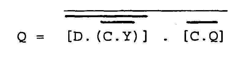
gates 5 and 6 performing the function:
gates 7 and 8 performing the function
- The transparent latch of Fig 2 operates as follows:
- There are two modes of operation. When the control input C is low, the latch is transparent with the output Q following the input D. When C is high, the output Q is latched at the value that existed before C changed state i.e. Qo. In this Latter, "inhibit" mode any changes in D are prevented from getting through to the output.
- Referring now to the truth table in conjunction with Fig 2. Under
conditions 1 and 2 i.e an "enable" condition, with the control input C low, the outputs ofgates - Under
conditions 3 and 4, control input C is now high (which is an inhibit condition) and the value of D remains as it was before any change of state of C (ie D = Qo). Taking the case where D=1, when C changes from low to high, there will be no change of state in the outputs ofgates 5 and 6, butgate 7 output will change to low. However, with Y still held low, gate 8 will maintain Q high. - Under condition 4 where D=0, when C changes from low to high, the output of
gate 5 will go low. However with D low, Y is maintained high at the output of gate 6. The output states ofgates 7 and 8 remain as they were when C was low and so Q is maintained low. -
Conditions 5 and 6 refer to situations where C is set to high ie inhibit and the level of D changes while C is still high. These changes are blocked from reaching the output Q by the action of the gates as explained below. - When D moves from high to low, both
gates 5 and 6 change their output states, with Y moving from low to high. However, because the second input of gate 8 is low, the change in Y is blocked from getting through and altering the state of the output Q. Hence, due to the combined actions ofgates 7 and 8 Q remains latched at Qo (high). - Finally, under condition 6 when D moves from low to high,
gates 5 and 6 ensure that this change cannot be propagated. Thus Y remains high with no possible changes to the states ofgates 7 and 8. Hence Q remains latched at Qo (low). - While the transparent latch of the specific example has been configured using four NAND gates, it will be appreciated by those skilled in the art that other combinations of gates whose Boolean functions are identical with that of the circuit of Fig 2 will achieve the same result.
- From Figure 2 it will be noted that the latch consists of two pairs of logic gates in which the output of each gate comprising a pair is fed back to an input of the other gate comprising the same pair. Also that the control input C is applied to both pairs, with the signal input D being applied to just a first pair, and the output of the first pair being applied to an input of the second pair.
Claims (5)
- A transparent latch comprising four logic gates (5, 6, 7 and 8) in which,
a first input to the second gate (6) is arranged to receive a signal input (D),
an input to the first gate (5) is arranged to receive a control input (C) to determine whether the latch will be in a first operating mode in which the logic state of the signal input (D) will propagate to an output (Q), or in a second operating mode in which any logic level change in the signal input (D) will be blocked from reaching the output (Q),
an output from the second gate (6) and an output from the third gate (7) are connected to respective inputs to the fourth gate (8),
and the output (Q) from the fourth gate (8) is connected to a first input to the third gate (7),
characterised in that the output (Y) from the second gate (6) is connected to another input to the first gate (5),
an output from the first gate (5) is connected to a second input to the second gate (6), and the control input (C) is connected to an input of the third gate (7). - A transparent latch, according to Claim 1, in which the logic gates (5, 6, 7, and 8) are NAND gates.
- A transparent latch, according to Claim 2, in which the first gate (5) and the second gate (6) perform the function

- A transparent latch, according to Claims 2 or 3, in which the third gate (7) and the fourth gate (8) perform the function

- A transparent latch, according to Claims 3 and 4, in which the logic gates (5, 6, 7 and 8) are selected and interconnected to operate with the Boolean function

Applications Claiming Priority (3)
| Application Number | Priority Date | Filing Date | Title |
|---|---|---|---|
| GBGB9523393.8A GB9523393D0 (en) | 1995-11-16 | 1995-11-16 | Logic circuits |
| GB9523393 | 1995-11-16 | ||
| PCT/GB1996/002815 WO1997018629A1 (en) | 1995-11-16 | 1996-11-15 | Logic circuits |
Publications (2)
| Publication Number | Publication Date |
|---|---|
| EP0875092A1 EP0875092A1 (en) | 1998-11-04 |
| EP0875092B1 true EP0875092B1 (en) | 2006-05-31 |
Family
ID=10783944
Family Applications (1)
| Application Number | Title | Priority Date | Filing Date |
|---|---|---|---|
| EP96938370A Expired - Lifetime EP0875092B1 (en) | 1995-11-16 | 1996-11-15 | Logic circuits |
Country Status (6)
| Country | Link |
|---|---|
| US (1) | US6249163B1 (en) |
| EP (1) | EP0875092B1 (en) |
| AU (1) | AU720687B2 (en) |
| DE (1) | DE69636198T2 (en) |
| GB (2) | GB9523393D0 (en) |
| WO (1) | WO1997018629A1 (en) |
Cited By (2)
| Publication number | Priority date | Publication date | Assignee | Title |
|---|---|---|---|---|
| US10229748B1 (en) | 2017-11-28 | 2019-03-12 | International Business Machines Corporation | Memory interface latch with integrated write-through function |
| US10381098B2 (en) | 2017-11-28 | 2019-08-13 | International Business Machines Corporation | Memory interface latch with integrated write-through and fence functions |
Families Citing this family (3)
| Publication number | Priority date | Publication date | Assignee | Title |
|---|---|---|---|---|
| JP5807333B2 (en) * | 2011-01-27 | 2015-11-10 | ソニー株式会社 | Delay latch circuit and delay flip-flop |
| CN104658508B (en) * | 2015-03-24 | 2017-06-09 | 京东方科技集团股份有限公司 | A kind of shift register cell, gate driving circuit and display device |
| CN104835443B (en) * | 2015-06-03 | 2017-09-26 | 京东方科技集团股份有限公司 | A kind of shifting deposit unit, gate driving circuit and display device |
Family Cites Families (9)
| Publication number | Priority date | Publication date | Assignee | Title |
|---|---|---|---|---|
| US4002933A (en) * | 1975-02-18 | 1977-01-11 | Texas Instruments Incorporated | Five gate flip-flop |
| US4156154A (en) * | 1976-12-14 | 1979-05-22 | Tokyo Shibaura Electric Co., Ltd. | Flip-flop circuit |
| NL8502811A (en) * | 1985-10-15 | 1987-05-04 | Philips Nv | INTEGRATED MEMORY CIRCUIT. |
| US5004933A (en) * | 1986-06-02 | 1991-04-02 | Tektronix, Inc. | Phase-selectable flip-flop |
| JPS6413808A (en) * | 1987-07-08 | 1989-01-18 | Mitsubishi Electric Corp | Latching circuit |
| DE3813138C2 (en) | 1988-04-20 | 1996-08-22 | Teves Gmbh Alfred | Valve block assembly |
| DE3813816C2 (en) * | 1988-04-23 | 1995-11-23 | Daimler Benz Aerospace Ag | Gate circuit |
| US4864161A (en) * | 1988-05-05 | 1989-09-05 | Altera Corporation | Multifunction flip-flop-type circuit |
| US5781053A (en) * | 1996-08-21 | 1998-07-14 | Advanced Micro Devices Inc. | Positive edge triggered flip flop |
-
1995
- 1995-11-16 GB GBGB9523393.8A patent/GB9523393D0/en active Pending
-
1996
- 1996-11-15 AU AU75820/96A patent/AU720687B2/en not_active Expired
- 1996-11-15 GB GB9623765A patent/GB2307365B/en not_active Expired - Fee Related
- 1996-11-15 DE DE69636198T patent/DE69636198T2/en not_active Expired - Lifetime
- 1996-11-15 WO PCT/GB1996/002815 patent/WO1997018629A1/en not_active Ceased
- 1996-11-15 EP EP96938370A patent/EP0875092B1/en not_active Expired - Lifetime
-
1998
- 1998-05-18 US US09/080,212 patent/US6249163B1/en not_active Expired - Lifetime
Cited By (3)
| Publication number | Priority date | Publication date | Assignee | Title |
|---|---|---|---|---|
| US10229748B1 (en) | 2017-11-28 | 2019-03-12 | International Business Machines Corporation | Memory interface latch with integrated write-through function |
| US10381098B2 (en) | 2017-11-28 | 2019-08-13 | International Business Machines Corporation | Memory interface latch with integrated write-through and fence functions |
| US10916323B2 (en) | 2017-11-28 | 2021-02-09 | International Business Machines Corporation | Memory interface latch with integrated write-through and fence functions |
Also Published As
| Publication number | Publication date |
|---|---|
| US6249163B1 (en) | 2001-06-19 |
| EP0875092A1 (en) | 1998-11-04 |
| GB9523393D0 (en) | 1996-01-17 |
| DE69636198T2 (en) | 2007-03-08 |
| GB2307365A (en) | 1997-05-21 |
| AU720687B2 (en) | 2000-06-08 |
| DE69636198D1 (en) | 2006-07-06 |
| GB2307365B (en) | 1997-12-03 |
| WO1997018629A1 (en) | 1997-05-22 |
| AU7582096A (en) | 1997-06-05 |
| GB9623765D0 (en) | 1997-01-08 |
Similar Documents
| Publication | Publication Date | Title |
|---|---|---|
| EP0456399B1 (en) | Logic module with configurable combinational and sequential blocks | |
| JP2735034B2 (en) | Clock signal distribution circuit | |
| EP1535394B1 (en) | Loosely-biased heterogeneous reconfigurable arrays | |
| US4504924A (en) | Carry lookahead logical mechanism using affirmatively referenced transfer gates | |
| EP0493835A2 (en) | An arithmetic operation unit having bit inversion function | |
| EP1236278B1 (en) | Method and apparatus for an n-nary logic circuit | |
| EP0653702A1 (en) | Carry chain adder using regenerative push-pull differential logic | |
| US5818747A (en) | Small, fast CMOS 4-2 carry-save adder cell | |
| US5020013A (en) | Bidirectional variable bit shifter | |
| EP0098692A2 (en) | Apparatus for adding first and second binary operands | |
| JP3248743B2 (en) | High-speed overflow / underflow limiter for signed adders | |
| EP0238091A2 (en) | Logic circuit | |
| US7170317B2 (en) | Sum bit generation circuit | |
| AU720687B2 (en) | Logic circuits | |
| US4092522A (en) | 5-Bit counter/shift register utilizing current mode logic | |
| US5329181A (en) | Complementary macrocell feedback circuit | |
| US6731138B2 (en) | Circuits and methods for selectively latching the output of an adder | |
| US6219686B1 (en) | Method and apparatus for an N-NARY sum/HPG adder/subtractor gate | |
| EP1698054B1 (en) | Circuit element | |
| US6661812B1 (en) | Bidirectional bus for use as an interconnect routing resource | |
| US6219687B1 (en) | Method and apparatus for an N-nary Sum/HPG gate | |
| US4584660A (en) | Reduction of series propagation delay and impedance | |
| JPH0679269B2 (en) | Adder | |
| KR950007464B1 (en) | Full adder | |
| EP1081590A1 (en) | An incrementer/decrementer having a reduced fan-out architecture |
Legal Events
| Date | Code | Title | Description |
|---|---|---|---|
| PUAI | Public reference made under article 153(3) epc to a published international application that has entered the european phase |
Free format text: ORIGINAL CODE: 0009012 |
|
| 17P | Request for examination filed |
Effective date: 19980817 |
|
| AK | Designated contracting states |
Kind code of ref document: A1 Designated state(s): DE ES FR GB IT SE |
|
| 17Q | First examination report despatched |
Effective date: 20000420 |
|
| APAB | Appeal dossier modified |
Free format text: ORIGINAL CODE: EPIDOS NOAPE |
|
| APAB | Appeal dossier modified |
Free format text: ORIGINAL CODE: EPIDOS NOAPE |
|
| RAP1 | Party data changed (applicant data changed or rights of an application transferred) |
Owner name: BAE SYSTEMS PLC |
|
| APBT | Appeal procedure closed |
Free format text: ORIGINAL CODE: EPIDOSNNOA9E |
|
| GRAP | Despatch of communication of intention to grant a patent |
Free format text: ORIGINAL CODE: EPIDOSNIGR1 |
|
| APAA | Appeal reference recorded |
Free format text: ORIGINAL CODE: EPIDOS REFN |
|
| RAP1 | Party data changed (applicant data changed or rights of an application transferred) |
Owner name: MBDA UK LIMITED |
|
| GRAS | Grant fee paid |
Free format text: ORIGINAL CODE: EPIDOSNIGR3 |
|
| APAF | Appeal reference modified |
Free format text: ORIGINAL CODE: EPIDOSCREFNE |
|
| GRAA | (expected) grant |
Free format text: ORIGINAL CODE: 0009210 |
|
| AK | Designated contracting states |
Kind code of ref document: B1 Designated state(s): DE ES FR GB IT SE |
|
| PG25 | Lapsed in a contracting state [announced via postgrant information from national office to epo] |
Ref country code: IT Free format text: LAPSE BECAUSE OF FAILURE TO SUBMIT A TRANSLATION OF THE DESCRIPTION OR TO PAY THE FEE WITHIN THE PRESCRIBED TIME-LIMIT;WARNING: LAPSES OF ITALIAN PATENTS WITH EFFECTIVE DATE BEFORE 2007 MAY HAVE OCCURRED AT ANY TIME BEFORE 2007. THE CORRECT EFFECTIVE DATE MAY BE DIFFERENT FROM THE ONE RECORDED. Effective date: 20060531 |
|
| REG | Reference to a national code |
Ref country code: GB Ref legal event code: FG4D |
|
| REF | Corresponds to: |
Ref document number: 69636198 Country of ref document: DE Date of ref document: 20060706 Kind code of ref document: P |
|
| PG25 | Lapsed in a contracting state [announced via postgrant information from national office to epo] |
Ref country code: ES Free format text: LAPSE BECAUSE OF FAILURE TO SUBMIT A TRANSLATION OF THE DESCRIPTION OR TO PAY THE FEE WITHIN THE PRESCRIBED TIME-LIMIT Effective date: 20060911 |
|
| REG | Reference to a national code |
Ref country code: SE Ref legal event code: TRGR |
|
| ET | Fr: translation filed | ||
| PLBE | No opposition filed within time limit |
Free format text: ORIGINAL CODE: 0009261 |
|
| STAA | Information on the status of an ep patent application or granted ep patent |
Free format text: STATUS: NO OPPOSITION FILED WITHIN TIME LIMIT |
|
| 26N | No opposition filed |
Effective date: 20070301 |
|
| REG | Reference to a national code |
Ref country code: FR Ref legal event code: PLFP Year of fee payment: 20 |
|
| PGFP | Annual fee paid to national office [announced via postgrant information from national office to epo] |
Ref country code: DE Payment date: 20151119 Year of fee payment: 20 Ref country code: GB Payment date: 20151118 Year of fee payment: 20 Ref country code: IT Payment date: 20151124 Year of fee payment: 20 |
|
| PGFP | Annual fee paid to national office [announced via postgrant information from national office to epo] |
Ref country code: FR Payment date: 20151119 Year of fee payment: 20 Ref country code: SE Payment date: 20151118 Year of fee payment: 20 |
|
| REG | Reference to a national code |
Ref country code: DE Ref legal event code: R071 Ref document number: 69636198 Country of ref document: DE |
|
| REG | Reference to a national code |
Ref country code: GB Ref legal event code: PE20 Expiry date: 20161114 |
|
| PG25 | Lapsed in a contracting state [announced via postgrant information from national office to epo] |
Ref country code: GB Free format text: LAPSE BECAUSE OF EXPIRATION OF PROTECTION Effective date: 20161114 |