The present invention relates to a method of and
apparatus for digital video signal recording/reproducing.
An embodiment of the invention relates to an apparatus
for recording a digital video signal to a record medium and
reproducing a digital video signal from a record medium,
and a method thereof.
A signal processing apparatus that digitally
processes a video signal (for example, a signal
processing apparatus for use with a digital VTR (Video
Tape Recorder) that records/reproduces a high
resolution video signal) performs a picture compressing
and encoding process for an input picture signal. The
compressed and encoded video signal is recorded to for
example a video tape.
As compressing and decoding methods for
interlaced video signals, an intra-frame encoding
process and an intra-field encoding process are known.
The compression efficiency of the intra-field encoding
process is generally inferior to the compression
efficiency of the intra-frame encoding process. Since
the information amount of a high resolution video
signal is around five times larger than the information
amount of a standard resolution video signal, the
intra-frame compressing process should be used.
In a digital VTR, pictures can be edited in
individual frames. However, pictures based on a movie
film may be edited. Thus, the necessity for editing
pictures in individual fields is high. For example,
when a movie material with a format of 25 frames/sec is
converted into a video signal with a format of 30
frames/sec, a scene change may take place in two fields
of the same frame. In this case, a picture should be
edited in each field.
In addition to an editing method using two
VTRs (a recording VTR and a reproducing VTR), another
editing method using one VTR is often used. In the
latter method, a picture reproduced from a tape and a
picture to be input to the VTR are edited. The edited
picture is recorded. The editing method for editing
pictures in individual fields with one VTR is referred
to as field editing method.
When the field editing method is performed in
the intra-frame compressing and encoding process
(namely, a picture should be edited at the end of a
field), a frame may contain pictures that scarcely
correlate with each other in the fields, for example.
Namely, when the intra-frame compressing and encoding
process is performed, the compressing efficiency may
not be improved. In addition, since a picture is
compressed in each frame, an output signal of the error
correction decoder cannot be edited in each field.
An embodiment of the present invention seeks to
provide a digital video signal recording/reproducing
apparatus that allows pictures to be edited in individual
fields and that prevents the compressing efficiency from
being deteriorated.
One aspect of the present invention is a digital video
signal recording/reproducing apparatus for recording a
digital video signal to a record medium and reproducing a
digital video signal from a record medium, comprising:
Another aspect of the present invention is a digital
video signal recording/reproducing method for recording a
digital video signal to a record medium and reproducing a
digital video signal from a recording medium, comprising
the steps of:
In the digital VTR, decompressed video data
is sent back to a switching means of the recording
system. The switching means switches between
reproduced data and input data at the end of each
field. Thus, a field editing process can be
accomplished for a digital VTR. In the compressing and
encoding process, the intra-field encoding process or
the intra-frame encoding process can be selected. When
information that represents the selected encoding
process is recorded, even if a picture largely varies
at the end of a field, the compressing efficiency can
be prevented from being deteriorated.
A better understanding of the present invention will
become more apparent from the following illustrative
description thereof which is to be read in connection with
the accompanying drawings, in which:-
Next, with reference to the accompanying
drawings, a digital VTR according to an embodiment of
the present invention will be described. The digital
VTR according to the embodiment of the present
invention records a high resolution video signal and
reproduces a high resolution video signal from a
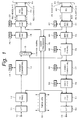
magnetic tape. Fig. 1 shows an example of the
structure of a recording system and a reproducing
system according to the embodiment of the present
invention.
Referring to Fig. 1, a serial digital A/V
signal with a data rate of 1.485 Gbps (bits per second)
corresponding to BTA S-004 standard is supplied to an
input terminal 10. The serial digital A/V signal is
sent to an S/P (serial to parallel) converter 11. The
serial signal sent to the S/P converter 11 is converted
into parallel data composed of a brightness signal Y
and color difference signals Pr and Pb. Each of the
brightness signal Y and color difference signals Pr and
Pb is composed of for example eight bits. The data
clock frequency of the parallel digital video signal is
74.25 MHz.
The parallel data is sent from the S/P
converter 11 to a coprocessor 12. The coprocessor 12
is composed of for example one ASIC (Application
Specific Integrated Circuit). The coprocessor 12
performs a process for auxiliary data and thereby
separates a digital audio signal, a line number LN, and
EAV from the serial data. The digital audio signal is
sent to an audio processor 16. The coprocessor 12
performs a CRC checking operation with a CRC redundant
code so as to determine whether or not an error takes
place on the transmission line (namely, a transmission
error). Alternatively, the CRC checking operation may
be performed in a format converter 13 disposed in the
next stage of the coprocessor 12.
An output signal of the coprocessor 12 is
sent to the format converter 13. The format converter
13 performs a filtering process for compressing a (4 :
2 : 2) signal into a (3 : 1 : 1) signal. When the
coprocessor 12 detects an error, the format converter
13 determines whether a connection point of a signal
takes place with the continuity of successive line
numbers. The format converter 13 compresses the band
width of a signal. The format converter 13 is composed
of for example one ASIC. A memory 14 is connected to
the format converter 13. A timing generator 30
supplies clock signals with frequencies of 74.25 MHz
and 46.40625 MHz to the format converter 13.
The format converter 13 converts the (3 : 1 :
1) signal into two-channel data. In Fig. 1, for
simplicity, only one signal path is shown. In the
circuits downstream of the format converter 13, data is
processed for each channel. Data on each channel has a
data rate of 46.40625 MHz. In each line, line numbers
LN0 and LN1 are placed in channel data Ch0 and channel
data Ch1, respectively.
The parallel (4 : 2 : 2) signal is converted
into the signals Ch0 and Ch1 each of which has the
brightness signal Y and the color difference signals Pr
and Pb serially arranged. Thus, the clock frequency of
74.25 MHz can be decreased to 5/8 (namely, 46.40625
MHz). In addition, the brightness signal Y and the
color difference signals Pr and Pb can be processed at
the same clock frequency.
An output signal (of two channels) of the
format converter 13 is sent to a selector 15. When the
field editing process is performed, the selector 15
selects a self-reproduced signal instead of the output
signal (input video signal) of the format converter 13.
A control signal is sent to the selector 15. The
control signal causes the selector 15 to operate in
synchronization with the end of each field. In
reality, when the user designates an editing point in a
particular field, the control signal causes the
selector 15 to switch the input video signal to a
reproduced video signal corresponding to the editing
point. For simplicity, Fig. 1 shows the selector 15 as
an independent circuit block. However, the selector 15
is actually structured in an IC chip of the format
converter 13.
The video signal selected by the selector 15
is sent to a BRR (Bit Rate Reduction) encoder 18. A
memory 20 is connected to the BRR encoder 18. The BRR
encoder 18 performs a compressing and encoding process
that includes for example a DCT (Discrete Cosine
Transform) process, a quantizing process, and a
variable-length code encoding process. In this
example, the picture compressing rate is 1/4.4. In
addition, the BRR encoder 18 adaptively switches
between the intra-field compressing process and the
intra-frame compressing process. In addition, the BRR
encoder 18 shuffles DCT blocks.
The two-channel data that has been compressed
and encoded by the BRR encoder 18 is sent to an ECC
(Error Correction Code) encoder 22. In addition, the
digital audio signal of which a particular process has
been performed by the audio processor 16 is also sent
to the ECC encoder 22. A memory 23 is connected to the
ECC encoder 22.
The ECC encoder 22 encodes the digital audio
signal with a product code. Namely, the ECC encoder 22
encodes the digital audio signal with an outer code,
adds an ID portion that includes a sync block number
and various flags to each sync block recorded on a
tape, and then encodes the resultant signal with an
inner code. The range of the encoding process with the
inner code includes the ID portion. One sync block
includes the parity of the inner code and a sync signal
that represents the top portion thereof. One sync
block is the minimum data element that is recorded and
reproduced.
An output signal of the ECC encoder is sent
to a recording driver 24. Record data of one channel
is sent from the recording driver 24 to magnetic heads
A/C through a rotating transformer. Record data of the
other channel is sent from the recording driver 24 to
magnetic heads B/D through a rotating transformer. The
record data is recorded on a magnetic tape 25.
The recording system has a timing generator
30 that supplies a system clock signal corresponding to
an applied format such as 1125 lines/60 Hz format, 1125
lines/59.94 Hz format, or 525 lines/59.94 Hz format.
Corresponding to the system clock signal, a clock
signal necessary for the recording system is generated.
Next, the structure of the reproducing system
will be described. Signals recorded on the magnetic
tape 25 are reproduced by the reproducing magnetic
heads A/C and B/D. Thus, two-channel reproduction
signals are obtained. A reproduction signal A/C of one
channel is sent to an equalizer 40. A reproduction
signal B/D of the other channel is sent to the
equalizer 40. The equalizer 40 is disposed for each
channel. In addition, individual processes in the
downstream stages of the format converter 47 are
performed for each channel.
Output signals of the equalizer 40 are sent
to an ECC decoder 41. A memory 42 is connected to the
ECC decoder 41. The ECC decoder 41 corrects an error
of a signal received from the equalizer 40 with an
inner code of an error correction code. The inner code
is completed in one sync block. When an error can be
corrected with the inner code, the ECC decoder 41
corrects the error. When an error cannot be corrected
with the inner code, the ECC decoder 41 sets an error
flag at the position of the error. Thereafter, the ECC
decoder corrects an error of the signal with an outer
code. With reference to the error flag, the ECC
decoder 41 performs an erasure-correcting process for
the error. Thus, most errors can be corrected.
However, when a large error such as an error that takes
place in the longitudinal direction of the tape, the
ECC decoder 41 cannot correct the error. In this case,
the ECC decoder 41 detects an error in the error
detecting range of the outer code and sets a word error
flag to the position of an error word.
The error correcting decoder 41 outputs data
and word error flag as sync blocks corresponding to the
clock signal of 46.40625 MHz. An output signal of the
error correcting decoder 41 is sent to a BRR decoder
43. The clock signal of 46.40625 MHz is supplied from
the timing generator 30 to the BRR decoder 43. The BRR
decoder 43 performs an inverse DCT converting process
and a deshuffling process with a memory 44 and decodes
the compressed signal. The BRR decoder 43 performs an
intra-field decoding process/intra-frame decoding
process corresponding to the intra-field encoding
process/intra-field encoding process performed by the
BRR encoder 18. Information that represents the type
of the encoding process is placed in the ID portion of
each sync block.
An output signal of the BRR decoder 43 is
sent to a concealing circuit 45 along with the error
flag. The concealing circuit 45 is composed of for
example one ASIC. A memory 46 is connected to the
concealing circuit 45. The concealing circuit 45
conceals an error that the ECC decoder cannot correct
(such as a large error due to a scratch on the magnetic
tape 4) in the reproduction signal. For example, the
concealing circuit 45 interpolates in a predetermined
manner an error portion that has not been corrected.
For example, the BRR decoder 43 determines an error of
a DCT coefficient corresponding to the word error flag.
When a DC coefficient or a low order AC coefficient
that is a relatively important coefficient has an
error, the BRR decoder 43 does not decode such a DCT
block. In this case, the BRR decoder 43 sends the
conceal flag to the concealing circuit 45. The
concealing circuit 45 interpolates the relevant DCT
block.
An output signal of the concealing circuit 45
is sent to the format converter 47 and the selector 15
of the recording system. The selector 15 selects an
output signal of the concealing circuit 45 (namely, a
reproduced video signal). Thus, the field editing
process is performed.
The format converter 47 suppresses irregular
noise that takes place in the decompressing
process/compressing process of the BRR decoder or the
BRR encoder 18 of the recording system. The format
converter 47 performs a noise suppressing process
corresponding to the clock signal of 46.40625 MHz with
a memory 48.
The format converter 47 receives the clock
signals of 46.40625 MHz and 74.25 MHz from the timing
generator 30. The format converter 47 converts the
two-channel signals into a (4 : 2 : 2) signal
corresponding to the clock signals with the memory 48.
The format converter 47 adds a line number to the
converted signal. The format converter 47 sends the
resultant signal with a data rate of 74.25 MHz to a
video processor 49.
A memory 50 is connected to the video
processor 49. The video processor 49 adjusts a gain,
an offset, and so forth of the received video signal.
An output signal of the video processor 49 is sent to a
coprocessor 51. In addition, reproduced audio data is
sent from the audio processor 16 to the coprocessor 51.
The audio data is decoded with an error correction code
by the ECC decoder 41 and then sent to the audio
processor 16. The audio processor 16 performs a
particular process for the audio signal and sends the
resultant signal to the coprocessor 51.
The coprocessor 51 places the digital audio
signal in the (4 : 2 : 2) signal corresponding to the
clock signal of 74.25 MHz and adds predetermined
auxiliary data corresponding to the relevant format to
the resultant signal. For example, the coprocessor 51
performs a CRC calculation for each line of the
resultant signal and generates a CRC code. With the
CRC code, a transmission error can be detected. An
output signal of the coprocessor 51 is sent to a P/S
(Parallel to Serial) converter 53. The P/S converter
53 converts the parallel signal into a serial digital
A/V signal with a data rate of 1.485 Gbps. An output
signal of the P/S converter 51 is sent as reproduced
serial data to an output terminal 54.
In the structure of the reproducing system,
an interface signal sent from the BRR decoder 43 to the
format converter 47 (composed of relevant ASICs) is
processed in the same format and corresponding to the
same clock signal (46.40625 MHz). Line numbers LN0 and
LN1 are added to the two-channel output signal of the
BRR decoder 43. The signal with the line numbers LN0
and LN1 is sent to the downstream circuits. Thus, even
if the continuity of the line numbers is lost, a
relevant error can be easily detected.
In the structure shown in Fig. 1, an output
signal of the concealing circuit 45 is sent back to the
selector 15 of the recording system. Alternatively,
another signal path for the field editing process may
be used. In other words, the output signal of the BRR
decoder 43 may be sent to the selector 15. In this
case, a picture signal that has not been interpolated
is recorded. Thus, a particular flag should be used so
that when the picture signal is output, it is
interpolated. As another alternative method, the video
processor 49 may send a processed video signal back to
the recording system (the preceding stage of the format
converter 13).
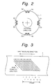
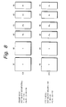
Fig. 2 shows an arrangement of rotating
heads. Fig. 3 shows a track pattern on a magnetic
tape. As shown in Fig. 2, four recording magnetic
heads 2A, 2B, 2C, and 2D are disposed on a rotating
drum 1 that rotates at for example 90 Hz. Double
azimuth heads are used so that the magnetic heads 2A
and 2B are adjacently disposed. The magnetic heads 2A
and 2B are composed of a double azimuth head so that
they are adjacently disposed. Likewise, the magnetic
heads are adjacently disposed. The azimuth angles of
the magnetic heads are different from each other.
Likewise, the azimuth angles of the magnetic heads 2C
and 2D are different from each other. The magnetic
head 2A is disposed opposite to the magnetic head 2C
(namely, with an angle of 180°). The magnetic head 2C
is disposed opposite to the magnetic head 2D (namely,
with an angle of 180°).
A magnetic tape is wound around the rotating
drum 1 with a winding angle of 180°. The magnetic
heads and the signal systems are switched so that a
record signal is sent and a reproduction signal is
obtained while the magnetic heads are tracking the
magnetic head. A point at which the magnetic heads and
the signal systems are switched is referred to as a
switching point. Now, assuming that tracks
corresponding to the heads are denoted by A, B, C, and
D, as shown in Fig. 3, the magnetic heads 2A and 2B
form the tracks A and B at the same time. In addition,
the magnetic heads 2C and 2D form the tracks C and D at
the same time.
A segment is composed of a pair of two
adjacent tracks (a pair of A and B channels and a pair
of C and D channels) that have different azimuth
angles. One frame (1/30 second) of a video signal is
composed of 12 tracks. Thus, one frame of a video
signal is composed of six segments. Six segments are
designated segment numbers 0 to 5. Audio data of four
channels is recorded at a center portion of each track
so that the audio data is sandwiched by video data.
Reproducing magnetic heads 3A, 3B, 3C, and 3D
are also disposed on the magnetic drum 1. The relation
of the arrangement and azimuth angles of the
reproducing magnetic heads 3A, 3B, 3C, and 3D is the
same as the relation of those of the recording magnetic
heads 2A, 2B, 2C, and 2D. According to an embodiment
of the present invention, when a reproduction signal is
sent back to the selector 15, a system delay takes
place from the beginning of the reproduction signal of
the tape to the beginning of a record signal to the
tape. For example, there is a system delay of six
fields.
In Fig. 2, for simplicity, the reproducing
magnetic heads 3A to 3D are disposed in advance of the
recording magnetic heads 2A to 2D by 90°, respectively.
Actually, the reproducing magnetic head 3A to 3D are
disposed in advance of the recording magnetic heads 2A
to 2D by an angle equivalent to the system delay,
respectively. Thus, a signal reproduced from the
magnetic tape 25 and a signal that has been field-edited
(the output signal of the selector 15) are newly
recorded in synchronization with a signal recorded on
the magnetic tape 25.
Fig. 4 shows an example of the BRR encoder
18. An output signal of the selector 15 is sent to a
shuffling circuit 61 and a mode determining circuit 62.
The mode determining circuit 62 determines a
compressing and encoding mode (field mode/frame mode)
and generates a mode ID. The mode ID is sent to the
shuffling circuit 61. The shuffling circuit 61
performs a block segmenting process for DCT blocks in a
field or DCT blocks in a frame corresponding to the
mode ID and shuffles DCT blocks with the external
memory 20.
An output signal of the shuffling circuit 61
is sent to a DCT circuit 63. The DCT circuit 63
performs a discrete cosine transforming process for the
signal received from the shuffling circuit 61 and
generates coefficient data. The coefficient data is
sent to a quantizing circuit 64. The quantizing
circuit 64 quantizes the coefficient data. The
quantizing circuit 64 controls a quantizing step so as
to generate a predetermined amount of data (namely, the
quantizing circuit 64 designates an amount of data
packed to a plurality of sync blocks or an amount of
data recorded to one track).
An output signal of the quantizing circuit 64
is sent to a variable-length code encoding circuit 65.
An output signal of the variable-length code encoding
circuit 65 is sent to a packing circuit 66. The
packing circuit 66 packs the signal received from the
variable-length code encoding circuit 65 to a sync
block. An output signal of the packing circuit 66 is
sent to the ECC encoder 22 (shown in Fig. 1).
Fig. 5 shows an example of the structure of
the mode determining circuit 62. In this circuit, with
the sum and variance of pixel values in each field, the
degree of the difference of two fields of one frame is
evaluated. An input signal of the mode determining
circuit 62 is sent to a switching circuit 71. The
switching circuit 71 sends data of two fields to
cumulating circuits 72 and 73. Each of the cumulating
circuits 72 and 73 obtains the sum of the pixel values
of each field. A subtracting circuit 76 obtains the
difference of the sums of the pixel values of the
individual fields.
A comparing circuit 77 compares the
difference with a threshold value 78 received from the
outside of the mode determining circuit 62. When the
difference is smaller than the threshold value, the
comparing circuit 77 generates a signal that represents
"0". When the difference is larger than the threshold
value, the comparing circuit 77 generates a signal that
represents "1". An output signal of the comparing
circuit 77 is sent to an OR gate 90.
In addition, an input signal of the mode
determining circuit 62 is sent to a square calculating
circuit 81. A switching circuit 82 sends an output
signal of the square calculating circuit 81 cumulating
circuits 83 and 84 corresponding to individual fields.
An output signal of the cumulating circuit 83 and an
output signal of the square calculating circuit 74 are
sent to a subtracting circuit 85. The subtracting
circuit 85 outputs the variance of the pixel values of
one field. Likewise, with the cumulating circuit 84, a
subtracting circuit 86, and a square calculating
circuit 75, the variance of the pixel values of the
other field is obtained.
The variances of the individual fields are
sent to a subtracting circuit 87. The subtracting
circuit 87 calculates the difference of these
variances. The difference of the variances is sent to
a comparing circuit 88. The comparing circuit 88
compares the difference with a threshold value 89
received from the outside of the mode determining
circuit 62. When the difference of the variances is
smaller than the threshold value, the comparing circuit
88 generates a signal that represents "0". When the
difference of the variances is larger than the
threshold value, the comparing circuit 88 generates a
signal that represents "1". An output signal of the
comparing circuit 88 is sent to the OR gate 90.
When the difference of the sums of the pixel
values of the individual fields is larger than the
relevant threshold value or when the difference of the
variances of the pixel values of the individual fields
is larger than the relevant threshold value, the OR
gate 90 generates a signal that represents "1".
Otherwise, the OR gate 90 generates a signal that
represents "0". When the OR gate 90 generates the
signal that represents "1", the mode determining
circuit 62 determines that the difference of pictures
in the individual frames is large. In other words, the
mode determining circuit 62 determines that the
movement of a picture is large and selects the intra-field
encoding process (field mode). When the OR gate
90 generates the signal that represents "0", the mode
determining circuit 62 determines that the difference
of the pictures in the frames is small. In other
words, the mode determining circuit 62 determines that
the movement of a picture is small and selects the
intra-frame encoding process (frame mode). In
addition, an output signal of the mode determining
circuit 62 (OR gate 90) is placed in the ID of each
sync block. The method for detecting the movement of a
picture in the fields is not limited to the above-described
method. Instead, various methods such as a
method using an average value and a method using the
sum of absolute values of differences between frames
can be used.
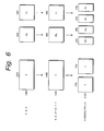
Fig. 6 is a schematic diagram showing a
compressing process for compressing the amount of data
of a high resolution video signal according to an
embodiment of the present invention. For example, the
high resolution video signal is a video signal
photographed by a high resolution video camera using a
CCD. The high resolution video signal is composed of
RGB components of three primary colors. The high
resolution signal is a (4 : 4 : 4) signal of which the
ratio of the sampling frequencies of these components
is 4 : 4 : 4. The RGB signal is converted into a
component signal ((4 : 2 : 2) signal) composed of a
brightness signal Y, a red color difference signal Pr,
and a blue color difference signal Pb.
One frame of a signal photographed by a high
resolution video camera is composed of 2200 H x 1125 V
pixels (where H represents the number of pixels in one
line; and V represents the number of pixels in one
frame). As represented by an upper portion of Fig. 6,
the signal Y (brightness signal) of the (4 : 2 : 2)
signal represents a valid area of the frame. The
signal Y is composed of 1920 H x 1080 V. Each of the
signals Pr and Pb is composed of 960 H x 1080 V. The
(4 : 2 : 2) signal and digital audio signal are sent as
serial data with a predetermined format to the input
terminal 10 of the recording system. In this format,
the audio data and additional data (error detecting
CRC. line number, and so forth) are sent using other
than the valid area.
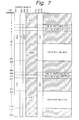
Fig. 7 shows a serial digital A/V signal with
a data rate of 1.485 Gbps corresponding to BTA S-004
standard that is an example of a transmission format of
serial data. In Fig. 7, numbers in the vertical
direction represent line numbers. Numbers in the
horizontal direction represent sample numbers. Data is
serially sent in the ascending order of line numbers
and picture sample numbers. Picture data and audio
data of one frame composed of 2200 samples in the
horizontal direction and 1125 lines in the vertical
direction are sent.
In the horizontal direction, 1920 samples
from 0-th sample to 1919-th sample are samples in a
valid picture area. In lines of other than a vertical
blanking interval, a video signal is sent. SAV that
represents the beginning of a valid picture area is
placed from the 2196-th sample to the 2199-th sample.
EAV that represents the end of a valid picture area is
placed from the 1920-th sample to the 1923-rd sample.
An audio signal is sent with 268 samples from the 1928-th
sample to the 2195-th sample. A line number LN is
placed in the 1924-th sample and the 1925-th sample. A
check bit of CRCC (Cyclic Redundancy Check Code) of
relevant lines is placed in the 1926-th sample and the
1927-th sample.
In the vertical direction, the 1-st line to
40-th line, the 558-th line to 602-nd line, and the
1121-st to 1125-th lines are vertical blanking
intervals. For example, a switching point of a helical
scan type video head is placed in a vertical blanking
interval. A video signal for one field is sent with
the 0-th sample to 1919-th sample in the 41-st line to
557-th line and the 603-rd line to 1120-th line.
As shown in Fig. 7, an audio signal is sent
in other than the next line of a switching point. In
this format, data and signal out of the valid picture
area in the horizontal direction is referred to as
auxiliary data.
The format converting circuit 13 (see Fig.
13) converts a (4 : 2 : 2) signal into a (3 : 1 : 1)
signal. As shown in Fig. 6, the signal Y of the (3 : 1
: 1) signal is composed of 1440 H x 1080 V. Each of
the signals Pr and Pb of the (3 : 1 : 1) signal is
composed of 480 H x 1080 V. In addition, the format
converting circuit 13 perform a demultiplexing process
(H-demultiplexing process) that separates the (3 : 1 :
1) signal into two channels in the horizontal
direction. Thus, as represented by a lower portion of
Fig. 6, the signal Y of each channel is composed of 720
H x 1080 V. Each of the signals Pr and Pb of each
channel is composed of 240 H x 1080 V.
In the downstream circuits of the format
converting circuit 13, individual processes are
performed for two channels. The data rate of the
serial data received from the input terminal 10 is
1.485 GHz. The S/P converter 11 converts the serial
data into parallel data with a data rate of 74.25 MHz.
The format converting circuit 13 outputs data with a
data rate of 44.4062 MHz (= 74.25 MHz x 5/8) for each
channel.
As described above, the BRR encoder 18 has
the field mode and the frame mode. In the field mode,
the BRR encoder 18 forms DCT blocks in a field and
performs the DCT encoding process for the DCT blocks.
In the frame mode, the BRR encoder 18 forms DCT blocks
in a frame and performs the DCT encoding process for
the DCT blocks. The information that represents the
field mode or frame mode is placed in the ID of each
sync block. When the difference of pictures of the two
fields of one frame is small (namely, the movement of a
picture is small), the frame mode is selected. On the
other hand, when the difference of pictures is large
(namely, the movement of a picture is large), the field
mode is selected. Fig. 8 shows a block segmenting
process for DCT blocks in the frame mode and the field
mode.
In the frame mode, a picture of one frame is
divided into DCT blocks of (8 H x 8 V) (Y) and (4 H x 8
V) (Pr/Pb). Thus, as represented by an upper portion
of Fig. 8, on each channel and in each frame, a (90 x
135) block (Y) and (60 x 135) blocks (Pr/Pb) are
formed. When DCT blocks are shuffled, for DCT blocks
(Pr/Pb), every two blocks are treated as a pair. Thus,
when DCT blocks are shuffled, a (30 x 135) block
(Pr/Pb) is formed.
On the other hand, in the field mode, a
picture of one frame is divided into DCT blocks of (8 H
x 4 V) (Y, Pr/Pb). The number of lines of each DCT
block is the half of that in the frame mode. This is
because the length of one DCT block in the field mode
is matched with that in the frame mode. Thus, as
represented by a lower portion of Fig. 8, on each
channel and in each frame, a (90 x 270) block (Y) and
(30 x 270) blocks (Pr/Pb) are formed. In these
structures of DCT blocks, DCT blocks are placed in
different positions from the original positions in the
frames. In other words, the DCT blocks are shuffled.
Thus, the amount of data that has been compressed and
encoded is averaged in DCT blocks.
Next, a data compressing process according to
an embodiment of the present invention will be
described with an example of the case that data of one
line is compressed. For example, as shown in Fig. 9A,
a video signal that is output from a CCD is a (4 : 4 :
4) signal of which a red signal R, a green signal G,
and a blue signal B are sent in parallel. Each of the
parallel signals has a data width of for example eight
bits. One pixel is composed of a set of Rn, Gn, and Bn
signals. Thereafter, the (4 : 4 : 4) signal is
converted into a (4 : 2 : 2) signal (see Fig. 9B). The
(4 : 2 : 2) signal is supplied in the format of serial
data shown in Fig. 7 from the input terminal 10. Data
shown in Fig. 9B is output from the coprocessor 12 that
decomposes the serial format.
The format converting circuit 13 converts the
(4 : 2 : 2) signal into a (3 : 1 : 1) signal (see Fig.
9C). The frequency of the clock signal of the (3 : 1 :
1) signal is 55.6875 MHz. In addition, the format
converting circuit 13 converts the (3 : 1 : 1) signal
into two-channel signals Ch0 and Ch1 of which the Y,
Pr, and Pb signals are arranged in serial. The
frequency of the clock signal of the signals Ch0 and
Ch1 is 46.40625 MHz (= 74.25 MHz x 5/8).
A line number LN is placed in each of the
signal Ch0 and Ch1. The line number LN is sent to each
structural portion along with data. When a signal is
processed, the line number LN is referenced for
controlling a memory address and a data order. Thus,
even if the continuity of lines is lost due to a
particular cause, data can be compensated in the order
of line numbers.
For simplicity of the compressing process,
Figs. 9A to 9D show only video data (V, Pr/Pb).
Fig. 10A shows an example of a (4 : 2 : 2)
with auxiliary data added by the coprocessor 12. A
brightness signal Y is successively sent corresponding
to the clock signal of 74.25 MHz. On the other hand,
since the band widths of the color difference signals
Pr and Pb have been compressed, the amount of data
thereof is halved. For example, brightness signals Y0
and Y1 correspond to color difference signals Pr0 and
Pb0, respectively. Brightness signals Y2 and Y3
correspond to color difference signals Pr1 and Pr2,
respectively.
Corresponding to a Hsync signal received from
the timing generator 30, SAV and EAV are placed at the
beginning and the end of 1920 clock pulses that
represent a valid picture area of the (4 : 2 : 2)
signal for four clock pulses each. After EAV, line
numbers LN0 and LN1 generated corresponding to a line
number LN are placed. Afer the line numbers LN0 and
LN1, CRC check bits CR0 and CR1 are placed. The CRC
check bits are added so as to detect an error of data
sent among each IC chip. Since the number of valid
lines in the vertical direction is 1125, a line number
LN can be represented by 11 bits.
Fig. 10B show two-channel data Ch0 and Ch1
that are output from the format converting circuit 13.
The period of the valid data in the signal is included
in the period of 1200 clock pulses. When a Hsync0
signal corresponding to the signal Ch0 goes high, the
Hsync0 signal represents the start of one horizontal
interval. The line numbers LN0 and LN1 are placed for
two clock pulses. Thereafter, the brightness signal Y
and the color difference signals Pr and Pb are serially
placed. After the brightness signal Y and the color
difference signals Pr and Pb for one line, a CRC check
bit is placed for one clock pulse. At the 1375-th
clock pulse of the Hsync signal at the beginning of one
horizontal interval, the next Hsync signal takes place.
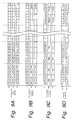
Fig. 11 shows a format of one track. This
track represents a data arrangement in the tracing
direction of a head. One track is largely divided into
a video sector V and an audio sector A. As will be
described later, video data and audio data in each
track are encoded with a product code. In Fig. 11, P
represents a parity of an outer code that takes place
when video data is encoded with a product code. A
parity of an outer code that takes place when audio
data is encoded with a product code is recorded in an
audio sector.
Fig. 11 shows an example of lengths of
individual types of data recorded in one track. In
this example, data of 275 sync blocks plus 124 bytes is
recorded in one track. A video sector is composed of
226 sync blocks. The time period of one track is
around 5.6 ms.
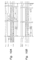
Fig. 12 shows an example of the structure of
an error correction code against video data. Video
data in each track is encoded with an error correction
code. In other words, video data for one rack is
arranged as 217 x 226 words. An encoding process is
performed for 226 words (one word is equal to one byte)
arranged in the vertical direction with (250, 226) Reed
Solomon code (namely, an outer code). A parity of an
outer code of 24 words is added. With the outer code,
an error correction of up to 10 words can be performed.
In addition, an erasure correction of up to 24 words
can be performed.
An ID of two words is added to 217 words
arranged in the horizontal direction of a two-dimensional
array (video data or parity of an outer
code). An encoding process is performed for (217 + 2 =
219) words arranged in the horizontal direction with
(231, 219) Reed Solomon code (inner code). Thus, a
parity of an inner code of 12 words is generated. With
the inner code, for example, an error of up to four
words is corrected. Alternatively, an erasure flag for
correcting an error with an outer code is generated.
As with video data, audio data is encoded
with a product code although the data amount of one
track of the video data is different from that of the
audio data.
Data is encoded with an outer code. The
resultant data with an ID is encoded an inner code.
Data is cut in the encoding direction of the inner
code. A block sync is added to the resultant data.
Thus, one sync block is formed. In other words, a
block sync of two words is added to (2 + 217 + 12 =
231) words of each line of the arrangement shown in
Fig. 12. On the magnetic tape, if necessary, data of
successive sync blocks is digitally modulated and then
recorded.
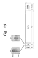
Fig. 13 shows the structure of one sync
block. An ID of a sync block is composed of two words
(two bytes) that are ID0 and ID1. ID0 represents a
sync block number. SBN0 represents LSB. SBN7
represents MSB. ID1 has the following bits.
The first one word of 217 words of each sync
block is a data header. A sync error flag of one bit
is placed in the data header along with information
that represents a quantizing characteristic of data.
The feature of the embodiment of the present
invention is in that a field editing process can be
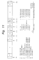
performed. Next, with reference to a timing chart
shown in Fig. 14, the recording/reproducing operation
and the field editing operation will be described. As
represented by an upper portion of Fig. 14, it is
assumed that the frame number varies in the order of
-2, -1, 0, 1, and so forth and that the field number
varies in the order of -4, -3, -2, -1, 0, 1, 2, 3, and
so forth. As will be described later, the selector 15
switches between the field numbers 0 and 1 of the frame
number 0 so as to select an input signal from a
reproduced signal.
Signals are obtained from reproducing heads.
One frame of the reproduced signals is composed of a
first channel of track numbers 1, 3, 5, 7, 9, and 11
(A/C) and a second channel of track numbers 2, 4, 6, 8,
10, and 12 (B/D). The ECC decoder 41 corrects an error
of a reproduced RF signal. The ECC decoder 41 takes a
correcting time for an outer code in each track. The
ECC decoder 41 adjusts the timing of each track.
An output signal of the ECC decoder 41 is
sent to the BRR decoder 41. The BRR decoder 43 decodes
a signal th a has been compressed and encoded. Since
the BRR decoder 43 de-shuffles data for one frame, a
delay for one frame takes place. The BRR decoder 43
outputs signals for original fields. The first field
and the second field reproduced from the tape are
denoted by PB#0 and PB#1, respectively.
An output signal of the BRR decoder 43 is
sent to the concealing circuit 45. After the
concealing circuit 45 has performed an interpolating
process for an error, it outputs the resultant signal
to a normal VTR reproducing system and a system for a
field editing process. The signal sent to the normal
reproducing system has a delay for the interpolating
process for several lines. The resultant signal is
sent to the output terminal 54 through the format
converter 47, the video processor 49, the coprocessor
51, and the P/S converter 53. The timing of the output
picture synchronizes with an external synchronous
signal of the VTR or an internal signal of the VTR.
In the system for the field editing process,
the concealing circuit 45 adjusts the delay against the
phase of the input video data and sends the resultant
signal to the selector 15 of the recording system. On
the other hand, a video signal received from the input
terminal 10 is sent to the selector 15 through the
coprocessor 12 and the format converter 13. The first
field and the second field of the input video data are
denoted by IN#0 and IN#1, respectively.
The selector 15 switches the output data from
the reproduced data to the input video data at the end
of a field of the frame 0. The selected output result
is a frame with a combination of PB#0 and IN#1.
Thereafter, an input picture is recorded.
The signal selected by the selector 15 is
compressed and encoded by the BRR encoder 18. In the
signal selected by the selector 15, when the movement
of pictures between the fields is large, the BRR
encoder 18 performs the intra-field compressing and
encoding process. When the movement of pictures is
small, the BRR encoder 18 performs the intra-frame
compressing and encoding process. Since the BRR
encoder 18 shuffles DCT blocks in each frame, it
outputs the resultant signal with a delay for one
frame.
After the signal received from the BRR
encoder 18 is encoded with an error correction code,
the resultant signal is recorded on a magnetic tape.
In this case, the ECC encoder 22 outputs the signal
with a delay for the calculating time of the outer
code. In the example shown in Fig. 14, the signal that
is output from the ECC encoder 22 has a delay for
around one track. On the tape, data is recorded in
such a manner that the original video data and the
input video data are connected. Thus, the field
editing process can be performed.
In the above embodiment, a controlling
operation for a signal delay in each stage was simply
described. However, delays in the concealing circuit
45, the format converter 13, and so forth should be
controlled so that the phase of the input picture
precisely accords with the phase of the reproduced
picture in the selector 15.
As described above, with the VTR that can
perform the field editing process, a pre-read editing
process can be easily performed. When a picture that
is reproduced from a tape is directly recorded, the
system for the field editing process can be used as it
is. When a picture reproduced from a tape is processed
(for example, after the gain of a picture is adjusted,
the resultant picture is recorded), a circuit for
sending an output signal of the video processor 49 back
to the selector of the recording system is provided.
As described above, an output signal of the
concealing circuit 45 or the BRR decoder 43 is sent
back to the selector of the recording system. The
reproducing heads are operated in advance of the
recording heads for a delay of the entire system (from
the reproducing heads to the recording heads). The
selector 15 switches between the reproduced data and
the input data at the end of each field. Thus, a
digital VTR that can perform the field editing process
can be structured. In addition, the BRR encoder 18 can
select either the intra-field encoding process or the
intra-frame encoding process. When information that
represents the selected encoding process is recorded on
the tape, even if a picture largely varies at the end
of a field, the efficiency of the compression does not
deteriorate.
In the block diagram shown in Fig. 1, each
function is represented as an error correcting encoder.
However, in reality, such functions are accomplished as
independent IC chips.
In the above embodiment, an example of which
the present invention is applied for the 1125 lines/60
Hz format was descried. However, the present invention
is not limited to such a format. For example, the
present invention can be applied for the NTSC format of
which the field frequency is 59.94 Hz. In this case,
each interface frequency and clock signal frequency is
divided by 1.001 (= 60/59.94).
In addition, the present invention can be
applied for a recording/reproducing system for only a
video signal.
illustrative embodiments of the present invention as
described above provide the following effects.
When the intra-frame compressing and encoding
process is used, the field editing process can be
performed.
Even if pictures that largely vary in the
fields of a frame are recorded, since the intra-field
compressing and encoding process or the intra-frame
compressing and encoding process can be adaptively
selected, pictures can be effectively recorded.
With a signal path for the field editing
process, the pre-read editing process of which a
reproduced picture is not edited can be performed.
Having described a specific preferred
embodiment of the present invention with reference to
the accompanying drawings, it is to be understood that
the invention is not limited to that precise
embodiment, and that various changes and modifications
may be effected therein by one skilled in the art
without departing from the scope or the spirit of the
invention.