Background of the invention
Field of the invention
The present invention relates to a multiplexing
system, provided in a line terminating unit of an ATM
switch which accommodates a plurality of physical
lines, which multiplexes fixed-length packets received
over input lines on an output line connected to an ATM
layer terminating apparatus, and more specifically to
a multiplexing system adapted for an arrangement in
which the bandwidth of the multiplexed output line is
equal to or greater than the sum of the bandwidths of
the input lines.
Description of the Related Art
In recent years, services have become
indispensable that uniformly handle various forms of
communications, including not only transmissions of
voice data and text data, but also transmissions of
image data for which higher transmission or bit rates
are required. As one of the major technologies that
help to conduct such communications services, the ATM
(asynchronous transfer mode) technique has been widely
used.
In the ATM, information is transmitted on a
cell-by-cell basis. Each cell consists of 48 octets
of payload, and 5 octets of control information
(including routing information) called the header.
Usually, ATM cells have their routes switched in
a switch to which incoming lines and outgoing lines
are connected. That is, upon receipt of a cell over
an incoming line, the switch outputs it onto an
outgoing line according to the routing information
carried in its header. Thus, the cell can be routed
to its destination.
The switch usually accommodates a large number of
lines. However, it is usual that the number of ports
(input ports or output ports) of a switching device
involved in actual switching is considerably smaller
than that of the lines accommodated, say, eight; this
is because high-speed processing is achieved by taking
advantage of statistical multiplexing. To input
incoming cells received over the many input lines into
the switching device, therefore, it is required to
multiplex the incoming cells. Methods of multiplexing
incoming lines include time-division multiplexing,
statistical multiplexing, etc. Here, "multiplexing
incoming lines" means, in this case, to multiplex
cells coming from the incoming lines.
In the time-division multiplexing, the sum of
bandwidths of input lines connected to a multiplexer
is equal to or less than the bandwidth of the output
line of the multiplexer, and each input line is
assigned a portion of the bandwidth of the output
line. The bandwidth assigned to each input line is
referred to as a slot on the time base. Each cell
inputted to the multiplexer over an input line is
output onto the output line in a state where it is
placed in the slot assigned to that input line.
The statistical multiplexing is generally applied
to the arrangement in which the sum of the bandwidths
of input lines of a multiplexer is greater than the
bandwidth of the output line. The statistical
multiplexing is a technique that employs the nature
that the timing of the peak of traffic on each input
line occurs at random and smoothes the peak of the
total traffic by multiplexing such input lines.
The statistical multiplexing has an advantage that
it can transmit large amounts of information with a
low bandwidth. However, when congestion occurs, cells
will be discarded. In order to avoid cells being
discarded, the statistical multiplexing needs very
complicated congestion control. With the
time-division multiplexing, however, although the
statistical multiplexing effect is not achieved, cells
will not be discarded when they are multiplexed
together. Thus, the time-division multiplexing is
used for multiplexing incoming cells while avoiding
cell congestion without complicated congestion
control.
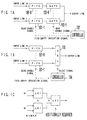
FIGs. 1A through 1C show block diagrams of a
conventional time-division multiplexer. FIG. 1A is
a block diagram of a WIRED-OR type multiplexer. Cells
received over input lines 1 to N are respectively
written into cell data storage FIFO memories 101-1 to
101-N. A controller 102 outputs read enable signals
to the FIFO memories 101-1 to 101-N and gates 103-1
to 103-N in a cyclic manner. Upon receipt of a read
enable signal from the controller 102, each of the
FIFO memories 101-1 to 101-N reads a cell out. Upon
receipt of the read enable signal from the controller
102, each of the gates 103-1 to 103-N outputs a cell
read out from the corresponding FIFO memory onto the
output line. The outputs of the respective gates
103-1 to 103-N are physically connected to a single
line (output line). In this way, the input lines 1
to N are selected in a cyclic manner and thus cells
received over the input lines are outputted in
sequence onto the output line formed by connecting the
gate outputs in a WIRED-OR connection.
When each of the FIFO memories is empty, it sends
a FIFO empty indication signal to the controller 102
to make notification that no cell is stored. The
controller 102 outputs no read enable signal to the
FIFO memory that is outputting the FIFO empty
indication signal.
FIG. 1B is a block diagram of a MUX type
multiplexer. This type of multiplexer is equipped
with a selector 105 on the output side of the FIFO
memories 101-1 to 101-N. A controller 104 outputs a
read enable signal to each of the FIFO memories in a
cyclic manner and outputs a select signal to the
selector 105. As with the WIRED-OR type multiplexer,
each of the FIFO memories is responsive to a read
enable signal to output a cell. The selector 105
selects an input line specified by the select signal
to output a cell received over the selected input line
onto the output line. In this way, each of the input
lines 1 to N is selected in a cyclical manner and a
cell received over the selected input line is sent
over the output line.
The conventional techniques have the following
drawbacks. In the WIRED-OR type, increasing the
number of input lines results in an increase in the
load capacitance associated with the output line
connected in a WIRED-OR connection, causing rounding
of pulse waveforms. As a result, cells from different
input lines will collide with one another, making
high-speed processing difficult.
In the MUX type, on the other hand, the selector
105 is installed independently of the circuits
associated with the input lines (the FIFO memories,
etc); thus, the multiplexer cannot flexibly adapt
itself to a change in the number of the input lines.
In addition, the MUX type multiplexer has a drawback
that, when a large number N of input lines are divided
into K groups of M lines (N = M × K) and an LSI is
used to service each group of M input lines as shown
in FIG. 1C, the multiplexing of N inputs will require
an additional LSI to combine the outputs of the K LSIs
into a multiplexed signal.
Summary of the Invention
It is an object of the present invention to
provide a high-speed multiplexing system which allows
a system modification to be accommodated flexibly.
A line multiplexing system of the present
invention is arranged to multiplex fixed length
packets received over input lines on an output line.
The line multiplexing system includes a plurality of
separate multiplexing units with which the input lines
are connected respectively and cascading lines that
connect the separate multiplexing units in cascade.
Each of the separate multiplexing unit multiplexes a
fixed length packet received from the upstream
cascading line and a fixed length packet received over
its associated input line, and sends the multiplexed
fixed length packets over its associated downstream
cascading line. Among the separate multiplexing units
connected in cascade, the most downstream separate
multiplexing unit provides a multiplexed output signal
on the output line.
A line multiplexing system of another embodiment
of the present invention multiplexes fixed length
packets received over input lines on a multiplexed
output line the bandwidth of which is equal to or
greater than the sum of the bandwidths of the input
lines. The line multiplexing system includes a
plurality of separate multiplexing units with which
the input lines are connected respectively, cascading
lines that connect the separate multiplexing units in
cascade, and a multiplexing permission signal
generating unit for generating a multiplexing
permission signal every period N × T where N is the
number of the input lines and T is the time required
to transfer one fixed length packet over the cascading
line, and outputting it onto the cascading lines. At
the time when the multiplexing permission signal is
received from the upstream cascading line, the
separate multiplexing unit sends a fixed length packet
received over its associated input line to the
downstream cascading line together with the
multiplexing permission signal. At the time when the
multiplexing permission signal is not received, the
separate multiplexing unit sends a fixed length packet
received from the upstream cascading line to the
downstream cascading line. Among the separate
multiplexing units connected in cascade, the most
downstream separate multiplexing unit provides a
multiplexed output signal on the output line.
Still another line multiplexing system of the
present invention is arranged to multiplex fixed
length packets received over input lines on a
multiplexed output line, the bandwidth of which is
equal to or greater than the sum of the bandwidths of
the input lines. The line multiplexing system
comprises separate multiplexing units with which the
input lines are connected respectively, a line
identification number being set up on each of the
separate multiplexing units to identify its associated
input line, cascading lines for connecting the
separate multiplexing units in cascade, and a packet
generation unit for generating a set of fixed length
packets each having tag information corresponding to
a respective one of the line identification numbers
added and sequentially sending each of the fixed
length packets over the cascading lines. When the
line identification number specified by the tag
information in a fixed length packet received from the
upstream cascading line coincides with the line
identification number for its associated input line,
the separate multiplexing unit sends a fixed length
packet received over its associated input line to the
downstream cascading line. When no coincidence
occurs, the separate multiplexing unit sends a fixed
length packet received from the upstream cascading
line to the downstream cascading line. Among the
separate multiplexing units connected in cascade, the
most downstream separate multiplexing unit provides
a multiplexed output signal on the multiplexed output
line.
Brief Description of the Drawings
FIG. 1A is a block diagram of a conventional
WIRED-OR type multiplexer;
FIGs. 1B and 1C are block diagrams of conventional
MUX type multiplexers;
FIG. 2 illustrates the principles of the present
invention;
FIG. 3 shows an arrangement of an ATM switch to
which a multiplexing arrangement of the present
invention is applied;
FIG. 4 shows an arrangement of a line terminating
unit;
FIG. 5 shows an embodiment of a multiplexing
arrangement of the present invention;
FIGs. 6A and 6B show signals transferred over the
cascading lines in the multiplexer of FIG. 5;
FIG. 7 shows another embodiment of the
multiplexing arrangement of the present invention;
FIGs. 8A and 8B show signals transferred over the
cascading lines in the multiplexer of FIG. 7;
FIG. 9 shows an arrangement of the input section
of FIG. 7;
FIG. 10 shows an arrangement of the token
generator of FIG. 9;
FIGs. 11A, 11B and 11C are diagrams for use in
explanation of the operation of a tag-based
multiplexing arrangement;
FIG. 12 shows an arrangement of the input section
in each separate multiplexing section in the tag-based
multiplexing arrangement;
FIG. 13A shows an arrangement of the tag
information memory of FIG. 12;
FIG. 13B shows the structure of a control cell;
FIG. 14 is a block diagram for explaining the
tag-based comparison processing in the tag
multiplexing arrangement;
FIGs. 15A and 15B show a method of transferring a
multiplexing timing indication signal in another type
of multiplexing arrangement;
FIG. 16A shows a multiplexing arrangement having
a function of reducing the effect of a failure on the
multiplexing arrangement;
FIG. 16B shows a bypassing facility; and
FIG. 17 shows another multiplexing arrangement
having a function of reducing the effect of a failure.
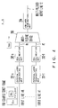
Detailed Description of the Preferred Embodiments
The basic configuration of a line multiplexing
system of the present invention will be described
below with reference to FIG. 2. The multiplexing
system of the present invention is configured such
that fixed length packets received over input lines
1-1 to 1-N are multiplexed together on an output line
2 and includes separate multiplexing sections or units
3-1 to 3-N which are respectively connected to the
input lines 1-1 to 1-N and cascading lines 4 which
connect the separate multiplexing units 3-1 to 3-N in
cascade. On the cascading line 4, data (including a
fixed length packet) are transmitted in one direction;
from separate multiplexing unit 3-1 to separate
multiplexing unit 3-2, from separate multiplexing unit
3-2 to separate multiplexing unit 3-3, ... . To
prevent fixed length packets from being discarded, the
sum of the bandwidths of the input lines 1-1 to 1-N
is set equal to or less than the bandwidth of the
output line 2.
Each separate multiplexing unit 3-i (i = 1, 2,...,
or N) multiplexes a fixed length packet received over
its upstream cascading line 4 and a fixed length
packet received over its associated input line 1-i
with the former given precedence over the latter and
outputs the resulting fixed length packet onto its
downstream cascading line 4. The separate
multiplexing unit 3-N that is the most downstream one
of the separate multiplexing units 3-1 to 3-N outputs
the multiplexed signals onto the output line 2.
In this manner, the input lines are connected in
cascade by the use of the separate multiplexing
sections each corresponding to a respective one of the
input lines, and a fixed length packet received over
each input line is multiplexed in turn. For this
reason, a change in the number of input lines can be
accommodated flexibly. In addition, since the
multiplexed output line is not connected in a WIRED-OR
connection, the multiplexing can be implemented at
high speed.
There are two methods of control as to which of a
packet received over the upstream cascading line and
a packet received over the corresponding input line
1-i connected to the separate multiplexing unit 3-i
is to select.
According to the first method, a multiplexing
enable signal is output over the cascading line 4
every period N × T where N is the number of input
lines and T is the time required to transfer a fixed
length packet over the cascading line. The separate
multiplexing unit 3-i is allowed to output a packet
received over the corresponding input line 1-i onto
its downstream cascading line only when it receives
the multiplexing enable signal over the cascading
line.
According to the second method, a number of fixed
length packets are produced each of which has tag
information added that corresponds to a respective one
of identification numbers that identify the input
lines 1-1 to 1-N and each of the packets is then sent
in turn over the cascading line. The separate
multiplexing unit 3-i is allowed to output a packet
received over the corresponding input line 1-i onto
its downstream cascading line only when the line
identification number specified by the tag information
carried in a packet received over its upstream
cascading line coincides with the identification
number of the corresponding input line 1-i.
The embodiments of the present invention will be
described below with reference to the drawings. In
the following, an ATM system is taken as an example
of an communications system to which the multiplexing
device of the present invention is applied.
FIG. 3 is a schematic illustration of an ATM
switch to which the multiplexing device of the present
invention is applied. The ATM switch accommodates a
number of input lines and a number of output lines and
outputs an incoming cell onto an output line in
accordance with routing information carried in the
header of that cell. Thus, the cell is routed to its
destination specified by the routing information.
Line terminating unit 11 terminates input lines #1
to #N. The input lines #1 to #N transmit, for
example, SONET frames. The line terminating unit 11,
as will be described later, has cell delineation units
for each of the input lines and a multiplexing unit
which multiplexes the output of the cell delineation
units. That is to say, the line terminating unit 11
delineates cells from data received over the input
lines and multiplexes the cells on the multiplexed
output line 12.
A statistical multiplexing unit 13 has its inputs
connected to a number of multiplexed output lines 12
and its output connected to a multiplexed input
highway to an ATM switch 14. In the statistical
multiplexing unit 13, cells on the multiplexed output
lines 12 are multiplexed statistically and then sent
to the ATM switch over the input highway. The sum of
the bandwidths of the multiplexed output lines 12
connected to the inputs of the statistical
multiplexing unit 13 is usually set equal to or
greater than that of the input highway. For example,
the bandwidth of the input highway is equal to that
of each multiplexed output line 12, i.e., 2.4 Gbps (=
2.4 GHz).
The switch 14 is a self-routing switch, which
outputs a cell transferred over an input highway on
an output highway specified by routing information
carried in the header. The cell on the output highway
is sent over an output line by distributors 15 and
line terminating unit 16.
The multiplexing device of the present embodiment
is provided in the line terminating unit 11.
FIG. 4 shows the configuration of the line
terminating unit 11 provided at the input terminal of
the ATM switch. Physical layer terminating units 201-1
through 201-n terminate input lines #1 through #N
respectively. The input lines #1 through #N transmit,
for example, a standardized data frame of SONET, etc.
The physical layer terminating units 201-1 through
201-n perform a synchronizing process and a warning
process on a received data frame, and extract the
payload. The payload stores an ATM cell.
Cell delineation units 202-1 through 202-n are
provided for the input lines #1 through #N
respectively, and detect ATM cells from the payload
extracted by each of the physical layer terminating
units 201-1 through 201-n using the HEC of each ATM
cell. At this time, the cells are synchronized.
A multiplexing device 203 multiplexes the output
from the cell delineation units 202-1 through 202-n.
A line connecting each of the cell delineation units
202-1 through 202-n to the multiplexing device 203 is
an input line to the multiplexing device 203. The
multiplexing device 203 refers to the multiplexing
system according to the present invention.
An ATM layer terminating device 204 performs a
routing process, an OAM (operation, administration,
and maintenance) process, etc. on an ATM cell output
from the multiplexing device 203, and transmits the
ATM cells on the multiplexed output line 12.
With the above described configuration, the
physical layer terminating unit and the cell
delineation unit should be provided for each input
line because they are operated based on the clocks
having different phases for respective input lines.
However, since the cells have been synchronized when
the ATM layer terminating unit receives the cells, all
input lines can be collectively processed.
Here, it is made a condition that the sum of the
bandwidths of the input lines #1 to #N (input lines
of the multiplexing device 203) is equal to or less
than the bandwidth of the multiplexed output line 12
(output line of the multiplexing device 203). In
other words, provided that the bandwidth (bit rate)
of the multiplexed output line 12 is determined,
limitations are imposed on the number of the input
lines and each of the bandwidths of the input lines
#1 to #N by the bandwidth of the multiplexed output
line. Assume, for example, that the bit rate of the
multiplexed output line is 2.4 Gbps (corresponding in
bandwidth to 2.4 GHz). Then, up to 16 input lines can
be accommodated when the bit rate of each input line
is 150 Mbps (corresponding in bandwidth to 150 MHz).
The multiplexing device 203 can be implemented in
several forms. The following description will be
given of a multiplexing system in which each of the
input lines #1 to #N is assigned the entire bandwidth
of the multiplexed output line and a multiplexing
system which can perform a statistical
multiplexing-like function.
FIG. 5 shows an example of a multiplexing device
of the present invention. This multiplexing device
has separate multiplexing sections 20-1 to 20-N with
which input lines #1 to #N are respectively
associated. The separate multiplexing sections are
connected in cascade as shown. Basically, the
separate multiplexing sections all have the same
arrangement. Here, the arrangement and operation of
the separate multiplexing section will be described
in terms of the separate multiplexing section 20-2.
A FIFO memory 21 stores a cell received over the
input line #2. That is, the cell transferred over the
input line #2 is written into the FIFO memory 21 at
the speed of the input line #2. Note that no idle
cell is written into the FIFO memory 21.
The separate multiplexing sections 20-1 to 20-N
are connected in cascade by cascading lines. The bit
rate of the cascading line is equal to that of the
multiplexed output line 12. Each of the separate
multiplexing sections receives not only a cell over
a respective corresponding one of the input lines but
also a cell from its adjacent upstream separate
multiplexing section over the cascading line. More
specifically, the separate multiplexing section 20-2
receives a cell sent from the separate multiplexing
section 20-1 over the cascading line that connects the
sections 20-1 and 20-2 together and the input line #2.
A failure monitor 22 detects a failure in the
cascading line. The failure monitor in the separate
multiplexing section 20-2 monitors the cascading line
between the separate multiplexing sections 20-1 and
20-2 to determine if a clock signal and a cell frame
signal are being transferred normally over that line.
A FIFO memory 23 stores a cell received over the
cascading line. More specifically, a cell received
over the cascading line between the separate
multiplexing sections 20-1 and 20-2 is written into
the FIFO memory 23 at the speed of that cascading
line. No idle cell is written into the FIFO memory
23.
A controller 24 issues a read enable signal to
read a cell out of the FIFO memory 21 or 23 and
controls a selector 25 so that the read cell is output
onto the cascading line. The controller 24 is
responsive to a FIFO-empty indication signal from the
FIFO memory 21 or 23 to determine whether a cell is
stored in the FIFO memory 21 or 23. Here, the
FIFO-empty signal goes high when no cell is stored in
the corresponding FIFO memory 21 or 23.
When one or more cells are stored in the FIFO
memory 23, the controller 24 reads one cell out from
the FIFO memory 23. When a cell is read out of the
FIFO memory 23, the controller 24 issues a select
signal to the selector 25 so that the output of the
FIFO memory 23 is selected. When there is no cell in
the FIFO memory 23, on the other hand, the controller
24 reads a cell out of the FIFO memory 21. In this
case, the controller 24 outputs a select signal to
cause the selector 25 to select the output of the FIFO
memory 21. When there is no cell in either of the
FIFO memories 21 and 23, the controller 24 outputs an
idle cell onto the cascading line.
Although, in the above arrangement, the cascading
line is assigned higher priority than the input line
in multiplexing cells, the input line may be assigned
higher priority.
In this manner, the separate multiplexing section
20-2 multiplexes cells received over the input line
#2 and the upstream cascading line connected to the
adjacent upstream separate multiplexing section 20-1
and sends the multiplexed cells to the adjacent
downstream separate multiplexing section 20-3 (not
shown) over the downstream cascading line. The cell
input to the separate multiplexing section 20-2 over
the upstream cascading line is one received over the
input line #1. That is, the separate multiplexing
section 20-i (the i-th separate multiplexing section
from the separate multiplexing section 20-1)
multiplexes cells input from the input lines
associated with the separate multiplexing sections
upstream of the separate multiplexing section 20-i and
a cell input from its associated input line #i and
sends those multiplexed cells to its adjacent
downstream separate multiplexing section over the
cascading line.
The separate multiplexing section 20-N, which is
located the most downstream of all the separate
multiplexing sections, multiplexes cells received over
all the input lines #1 to #N. The output line
connected to the separate multiplexing section 20-N
forms the multiplexed output line 12.
The separate multiplexing section 20-1, which is
located the most upstream of all the separate
multiplexing sections, will not receive any cell from
an upstream separate multiplexing section unlike the
other separate multiplexing sections 20-2 to 20-N.
For this reason, a dummy data generating section 26
is provided, which applies dummy data (an idle cell,
a clock signal, a cell frame signal, etc.) to the
separate multiplexing section 20-1. In each of the
separate multiplexing sections information is set as
to whether or not it is placed in the most upstream
position. The information may be set manually by
users or may be set automatically by a general control
unit (not shown) that controls every separate
multiplexing section.
As described above, the multiplexing device of the
present invention is arranged such that a number of
separate multiplexing sections, each of which
corresponds to a respective one of input lines, are
connected in cascade and the most downstream separate
multiplexing section provides an multiplexed output
of the multiplexing device. Thus, to multiplex a
number M (<= N) of input lines, these input lines need
merely be connected to M separate multiplexing
sections arbitrarily selected out of the separate
multiplexing sections 20-1 to 20-N. Suppose, for
example, that none of the input lines is connected to
the separate multiplexing section 20-2. When a cell
is stored in the FIFO memory 23, the controller 24
simply reads the cell out of the FIFO memory 23 and
outputs it; otherwise, the controller 24 simply
outputs an idle cell because, in this case, the FIFO
memory 21 is empty all the time. That is, the
separate multiplexing sections 20-1 to 20-N each act
as a FIFO memory (buffer memory) when no input line
is connected thereto. Thus, the multiplexing device
of the present embodiment can be adapted to any change
in the number of input lines to be multiplexed
together.
FIGs. 6A and 6B show signals transferred over the
cascading line in the multiplexing device of FIG. 5.
Here, description will be given in terms of input and
output signals of the separate multiplexing section
20-2.
On the cascading line cell data and control
signals are transferred in parallel. The control
signals comprise a clock signal, a cell frame signal,
and a cell enable signal. The clock signal has the
same frequency as a clock signal transferred over the
multiplexed output line 12. The cell frame signal
consists of pulses that appear at regular intervals
to indicate the beginning of the individual cells.
The cell enable signal goes to a high level when a
cell to be transferred is effective or a low level
when a cell to be transferred is an idle cell. The
cell data consists of a header and a payload
(including tag information under certain conditions)
and is transferred in synchronism with the clock
signal and the cell frame signal. The cell data is
transferred in 8-bit parallel form, by way of example.
The operation of the separate multiplexing section
20-2 will be described below. In the following
description, the times that define input timing are
represented by time slots T1, T2,..., and the times
that define output timing are represented by time
slots T11, T12,.... It is assumed here that no cell
has been stored in the FIFO memory 23 before the time
slot T1.
The separate multiplexing section 20-2 receives an
effective cell in the time slot T1. The effective
cell means that it is not an idle cell and here
corresponds to a cell received over the input line
#1 (#1 cell data). The input enable signal is high
in the time slot T1. Upon detecting that the input
cell enable signal is high in the time slot T1, the
separate multiplexing section 20-2 writes the cell
received over the cascading line in the time slot T1
into the FIFO memory 23. Upon detecting that a cell
is stored in the FIFO memory 23, the controller 24
reads the cell from the FIFO memory 23 regardless of
whether or not a cell is stored in the FIFO memory 21
and outputs it over the cascading line in the time
slot T11. In the time slot T11, the output enable
signal is high.
In the time slot T2, the separate multiplexing
section 20-2 receives an idle cell over the cascading
line. At this point, the input enable signal is low.
Thus, the idle cell received over the cascading line
is discarded without being written into the FIFO
memory 23. The FIFO memory 23 stores no cell because
the cell received in the time slot T1 has already been
read out. Upon detecting that the FIFO memory 23 is
empty, the controller 24 examines whether or not a
cell has been stored in the FIFO memory 21. Suppose
here that the FIFO memory 21 stores a cell. Then, the
controller 24 reads the cell out of the FIFO memory
21 and outputs it over the cascading line in the time
slot T12. The output enable signal is high in the
time slot T12.
Later the separate multiplexing section 20-2
receives an idle cell over the cascading line in the
time slot T3. This idle cell is also discarded
without being written into the FIFO memory 23. Upon
detecting that the FIFO memory 23 is empty, the
controller 24 examines whether or not a cell has been
stored in the FIFO memory 21. Suppose here that no
cell is stored in the FIFO memory 21. In this case,
since a cell to be read is not stored in either of the
FIFO memories 21 and 23, the controller 24 outputs an
idle cell over the cascading line in the time slot
T13. When an idle cell is output, the output enable
signal is set low.
Thus, if a cell is stored in the FIFO memory
connected to the cascading line, each of the separate
multiplexing sections 20-1 to 20-N reads the cell out
of the FIFO memory and outputs it. If, when no cell
is stored in the FIFO memory connected to the
cascading line, and when a cell is stored in the FIFO
memory connected to the corresponding input line, each
separate multiplexing section reads that cell out of
the FIFO memory and outputs it. If no cell is stored
in either of the FIFO memories, each separate
multiplexing section outputs, an idle cell. As a
result, in the most downstream separate multiplexing
section 20-N, cells received over the input lines #1
to #N are multiplexed together. Since the
multiplexing device of the present invention makes it
a condition that the sum of the bandwidths of the
input lines #1 to #N is equal to or less than the
bandwidth of the multiplexed output line 12, cells
from the input lines #1 to #N are multiplexed on the
multiplexed output line 12 without being discarded.
In addition, if there is an empty slot in a cell
data stream sent from the adjacent upstream separate
multiplexing section over the cascading line, each
separate multiplexing section can send a cell inputted
from the corresponding input line to its adjacent
downstream separate multiplexing section in that empty
slot. Here, the empty slot refers to a time interval
during which an idle cell is transferred. Thus, if,
under the circumstance that a plurality of cells are
stored in the FIFO memory connected to the
corresponding input line, empty slots appear in
succession in a cell data stream sent from the
adjacent upstream separate multiplexing section over
the cascading line, each separate multiplexing section
can output the cells stored in that FIFO memory in
succession to its adjacent downstream separate
multiplexing section using the empty slots.
By taking advantage of the above property, the
statistical multiplexing effect can be obtained. That
is, the condition that the sum of the bandwidths of
the input lines #1 to #N must not exceed the bandwidth
of the multiplexed output line 12 guarantees that,
even if cells are sent at the full rate over each
input line, none of the cells are discarded in the
multiplexing device 203. Under actual operating
conditions, however, a situation such that cells are
transferred at the full rate over all the input lines
cannot arise. Thus, idle cells will take up a
substantial portion of the output of the multiplexing
device 203. In other words, if, for example, the bit
rate of the multiplexed output line is 2.4 Gbps and
the bit rate of each input line is 150 Mbps, a maximum
of 16 input lines can only be accommodated under the
above condition. However, considering the statistical
multiplexing effect, it is expected that more than 16
input lines can be accommodated without discarding a
cell.
FIG. 7 shows an arrangement of another embodiment
of the multiplexing device of the present invention.
This multiplexing device has separate multiplexing
sections 30-1 to 30-N with which input lines are
respectively associated. As in the arrangement of
FIG. 5, the separate multiplexing sections are
connected in cascade by cascading lines. Basically,
the separate multiplexing sections each have the same
arrangement. Here, the arrangement and operation of
the separate multiplexing section will be described
in terms of the separate multiplexing section 30-2.
Like the FIFO memory 21 shown in FIG. 5, a FIFO
memory 31 temporarily stores a cell input over the
input line #2. An input section 32 receives cell data
and a control signal sent from the adjacent upstream
separate multiplexing section over the cascading line.
The input section 32 receives a master/slave signal
sent from a general control unit (not shown) that
controls the whole operation of the multiplexing
device 203, thereby determining whether or not the
separate multiplexing section 30-2 is the most
upstream one. When the separate multiplexing section
30-2 is not the most upstream one, the corresponding
input section 32 allows cell data and a control signal
sent from the adjacent upstream separate multiplexing
section to pass through as they are. When the
separate multiplexing section is the most upstream
one, on the other hand, the input section 32 produces
and outputs a cell frame signal and a token. The
arrangement of the input section 32 and the token will
be described later.
A controller 33 controls the outputting of a cell
from the corresponding separate multiplexing section
and produces a control signal to be sent to the
adjacent downstream separate multiplexing section.
That is, when a cell is received over the upstream
cascading line, the controller 33 controls a selector
34 so that the cell is immediately sent over the
downstream cascading line. In the absence of an
incoming cell from the cascading line, the controller
33 examines whether a cell is stored in the FIFO
memory 31. When a cell is stored in the FIFO memory
31, the controller 33 reads it out and then controls
the selector 34 so as to send it over the downstream
cascading line. Further, when no cell is received
over the upstream cascading line and the FIFO memory
31 is empty, the controller 33 outputs an idle cell
onto the downstream cascading line.
In this way, the separate multiplexing section
30-2, which remains basically unchanged from the
separate multiplexing section 20-2 in FIG. 5,
multiplexes cells inputted over the input line #2 and
the cascading line connected to the adjacent upstream
separate multiplexing section 30-1 and sends the
multiplexed cells to the adjacent downstream separate
multiplexing section 30-3 (not shown) over the
cascading line. That is, the separate multiplexing
section 30-i multiplexes a cell inputted over its
associated input line #i and cells inputted over the
input lines associated with the separate multiplexing
sections upstream of the section 30-i and sends the
multiplexed cells to the adjacent downstream separate
multiplexing section over the cascading line. In the
most upstream separate multiplexing section 30-N,
therefore, cells received over all the input lines #1
to #N are multiplexed together.
FIGs. 8A and 8B show signals transferred over the
cascading lines in the multiplexing device of FIG. 7.
Here, a description is given in terms of the separate
multiplexing section 30-2.
On the cascading line, cell data and control
signals are transferred in parallel. The control
signals include a token in addition to a clock signal,
a cell frame signal, and a cell enable signal that are
transferred in the arrangement of FIG. 5. In FIGs.
8A and 8B, the clock signal, the cell frame signal and
the cell enable signal are omitted.
The token is a signal that grants multiplexing
permission to the separate multiplexing sections 30-1
to 30-N. The token is produced in the most upstream
separate multiplexing section (the separate
multiplexing section 30-1 in the example of FIG. 7).
Upon receipt of the token, each separate multiplexing
section shifts the token by the duration of one time
slot and then sends it to the next separate
multiplexing section. One time slot refers to the
time required to transfer one cell over the cascading
line.
The operation of the separate multiplexing section
will be described now. Assume here that four input
lines (i.e., N = 4) are connected to the multiplexing
device of FIG. 7. Thus, the separate multiplexing
section 30-1 is the most upstream one and the separate
multiplexing sections 30-2 to 30-4 are connected in
cascade on the downstream side of the separate
multiplexing section 30-1. The master/slave signal
sets the separate multiplexing section 30-1 to the
master mode. The separate multiplexing sections 30-2
to 30-4 are each set to the slave mode. Further, the
number-of-input-lines indication signal notifies the
separate multiplexing section 30-1 that the number of
input lines is four.
Having confirmed that the number of input lines is
four, the separate multiplexing section 30-1 divides
the bandwidth of the cascading line into four. That
is, the separate multiplexing section 30-1 produces
a token every four time slots and sends it over the
cascading line simultaneously with cell data. As
shown in FIGs. 8A and 8B, the token is a pulse signal
the duration (width) of which corresponds to one time
slot. The bandwidth of the cascading line is the same
as that of the multiplexed output line 12.
As described previously, the token is a signal
that grants multiplexing permission to the separate
multiplexing sections 30-1 to 30-N. Thus, each
separate multiplexing section will obtain a right of
outputting one cell every four time slots.
The separate multiplexing section 30-2 receives an
output from the separate multiplexing section 30-1
over the cascading line (see FIG. 8A). Assuming the
times associated with input timing of the separate
multiplexing section 30-2 to be represented by time
slots T1, T2,.., the separate multiplexing section
30-2 receives the token in time slots T1, T5,.. These
time slots T1, T5,.. are ones assigned for the
separate multiplexing section 30-1. Although, in
FIGs. 8A and 8B, the first time slot of every four
time slots is labeled "#1 CELL DATA", these time slots
do not always hold a cell received over the input line
#1. If, in the time slots assigned for the separate
multiplexing section 30-1, no cell is stored in its
FIFO memory 31, then idle cells will be placed in
those time slots.
Upon receiving a token in the time slot T1, the
separate multiplexing section 30-2 outputs a cell data
received at the time slot T1 (#1 cell data) in the
time slot T11. However, the separate multiplexing
section 30-2 does not output a token in the time slot
T11.
The separate multiplexing section 30-2 judges that
the time slot next to the time slot (i.e., time slot
T1) in which the token has been transferred is the one
assigned to itself. In the time slot T12 next to the
time slot T11, the separate multiplexing section 30-2
reads a cell out of the FIFO memory 31, provided that
the memory is not empty, and then sends it over the
cascading line on the downstream side. If the FIFO
memory 31 is empty, the separate multiplexing section
30-2 outputs an idle cell onto the downstream
cascading line. The separate multiplexing section
30-2 outputs the token in the time slot T12. The
technique of outputting a token in synchronism with
a time slot is well known and remains unchanged from
the technique of producing a cell enable signal.
The time slots T3 and T4 are ones assigned for the
separate multiplexing sections 30-3 and 30-4,
respectively. In the time slots T13 and T14
corresponding to the time slots T3 and T4, therefore,
the separate multiplexing section 30-2 sends cell data
received from the adjacent upstream separate
multiplexing section 30-1 to the adjacent downstream
separate multiplexing section 30-3, as they were
received with no token outputted.
Thus, the multiplexing device of FIG. 7 divides
the bandwidth of the cascading line by the number of
input lines to obtain time slots, assigns each of the
time slots to a respective one of the input lines #1
to #N, and places cells received over the input lines
#1 to #N in the corresponding time slots, thereby
allowing cells received over the N input lines to be
multiplexed on one multiplexed output line. At this
point, the multiplexing timing of each separate
multiplexing section is controlled by a token. The
token system used in the present embodiment is
arranged such that, as described previously, each
separate multiplexing section presents the
multiplexing timing to the adjacent downstream
separate multiplexing section while shifting the
timing of the token. For this reason, there is no
need for any device that controls the multiplexing
timing for each of the separate multiplexing sections
30-1 to 30-N.
FIG. 9 shows a specific arrangement of the input
section 32 of FIG. 7. The arrangement of FIG. 9 is
common to the input sections of the separate
multiplexing sections 30-1 to 30-N.
The input section 32 receives a clock signal, a
cell frame signal, a cell enable signal, cell data,
and a token over the upstream cascading line. Note
here that the input section of the most upstream
separate multiplexing section (the separate
multiplexing section 30-1 in FIG. 7) receives those
signals from a dummy data generating section 26. The
input section 32 further receives a master/slave
signal and a number-of-input-lines indication signal
from the general control unit, not shown. The input
section 32 outputs a clock signal, a cell frame
signal, a cell enable signal, cell data, a token, and
an input interruption detect signal.
A clock detector 41 monitors the upstream
cascading line to determine if a clock signal is being
transferred normally. When an abnormal condition is
detected, the detector 41 issues an alarm signal,
which is, then applied to an OR circuit 44. The
abnormal conditions include a clock supply failure in
which the entry of a clock signal is not detected for
long than a fixed period of time and a clock frequency
error in which the clock frequency becomes offset with
respect to a given frequency. If the received clock
is normal, the clock detector 41 outputs it as it is.
A cell frame detector 42 monitors the upstream
cascading line to determine if a cell frame signal is
being transferred normally and, when an abnormal
condition is detected, issues an alarm signal. It is
considered abnormal when the interval at which cell
frame pulses arrive exceeds a given period of time.
The alarm signal is applied to the OR circuit 44. If
a cell frame signal received over the upstream
cascading line is normal, then the cell frame detector
42 applies it to a selector 46.
A token detector 43 monitors the upstream
cascading line to determine if tokens are being
transferred normally and, when an abnormal condition
is detected, issues an alarm signal. It is considered
abnormal when the interval at which the tokens arrive
exceeds a given period of time, which is defined, for
example, by the product of the duration of one time
slot and the number of input lines. The alarm signal
is entered into the OR circuit 44. In the input
section 32 in the most upstream separate multiplexing
section, however, the token detector 43 produces no
alarm signal. If a token received over the upstream
cascading line is normal, then the token detector 43
applies that token to a selector 48.
An output of the OR circuit 44 is used as an input
interruption signal. The way to employ this input
interruption signal will be described later. The cell
enable signal and cell data received over the upstream
cascading line are allowed to pass through the input
section 32 as they are.
A cell frame generator 45 generates a cell frame
signal, which is in turn applied to the selector 46
and a token generator 47. The cell frame generator
45 has a clock generator that generates a clock signal
with the same frequency as the clock signal
transferred over the cascading line, and a mod-k
counter. Here, k = 53, provided that a cell consists
of 53 bytes and cell data are transferred in parallel
on a byte-by-byte basis. Thus, the cell frame
generator 45 generates one clock pulse, i.e., a cell
frame signal, at intervals of the time required to
transfer one cell. The cell frame generator 45 may
be arranged to receive the above clock externally.
Such an arrangement will save the need for provision
of a clock generator for each input section.
Upon receipt of a master/slave signal at a 1 level
(indicating master), the selector 46 selects the cell
frame signal generated by the cell frame generator 45.
When the master/slave signal is at a 0 level
(indicating slave), the selector 46 selects a cell
frame signal received over the upstream cascading
line. That is, the most upstream separate
multiplexing section generates a cell frame signal by
itself, and the other separate multiplexing sections
each use a cell frame signal transferred from the
adjacent upstream separate multiplexing section.
When taught about the number of input lines
associated with the multiplexing device by the
number-of-input-lines indication signal, a token
generator 47 generates tokens to suit the number of
input lines. In FIG. 10 there is shown in block
diagram form an arrangement of the token generator 47.
A divide-by-N frequency divider 51 divides the
frequency of the cell frame signal by a factor of N.
The factor N, which is specified by the
number-of-input-lines indication signal, corresponds
to the number of input lines. Since the dividing
factor N is externally set, the divide-by-N frequency
divider 51 can divide the frequency of the cell frame
signal by an arbitrary integer. Thus, when a dividing
factor of four is specified by the
number-of-input-lines indication signal, the frequency
divider 51 produces one pulse signal each time it
receives four cell frame pulses. An output of the
frequency divider 51 is applied to a mod-k counter 52
as a timing indication signal.
Upon receipt of a timing indication signal, the
mod-k counter 52 starts a count operation to count the
rising edges of clocks up to k. Here, "k" is the same
as that described in connection with the cell frame
generator 45 and thus corresponds to the duration of
one time slot. For example, k = 53 when a cell
consists of 53 bytes and cell data are transferred in
parallel on a byte-by-byte basis. The mod-k counter
52 maintains its output at a high level for the
interval that elapses from the start of a counting
operation to the time when the rising edges of the
clocks have been counted up to k. A counter's output
signal at a high level is a token to be applied to the
selector 48 of FIG. 9.
When receiving a master/slave signal at a high
level (1) indicating master, the selector 48 selects
a token generated by the token generator 47. When
receiving a master/slave signal at a low level (0)
indicating slave, the selector 48 selects a token
received over the upstream cascading line. That is,
the most upstream separate multiplexing section
generates a token by itself, and the other separate
multiplexing sections each use a token received from
the adjacent upstream separate multiplexing section.
Thus, the input sections 32 of the separate
multiplexing sections 30-1 to 30-N have the same
arrangement, but they operate differently according
to the master/slave signal applied thereto, that is,
depending on whether or not they are placed in the
most upstream position.
Hereinafter, a modification of the multiplexing
device described with reference to FIGs. 7 to 10 will
be described. This multiplexing device is identical
in basic arrangement to that shown in FIG. 7 except
for the input section and the controller. The control
method used in this type of multiplexing arrangement
is called the tag method.
FIG. 11A - 11C are diagrams for use in explanation
of the operation of the tag-based multiplexing device.
Assume here that the number of input lines is four.
The most upstream separate multiplexing section
(corresponding to the separate multiplexing section
30-1 in FIG. 7) produces cells on which tag
information "1" to "4" are set up as shown in FIG. 11A
and places them in time slots in a cyclical manner.
Upon receipt of a cell on which tag information "1"
has been set up, the controller in the separate
multiplexing section 30-1 places a cell read out from
the FIFO memory connected to the input line #1 in the
time slot (indicated by "tag = #1) in which the cell
with tag information "1" has been placed. As a
result, cell data that is sent from the separate
multiplexing section 30-1 over the downstream
cascading line will contain that cell (#1 cell data)
received over the input line #1 every four time slots
as shown in FIG. 11B. That is, in the separate
multiplexing section 30-1, each time a cell on which
tag information "1" has been set up is received, a
cell received over the input line #1 is multiplexed
on the cascading line. If, when a cell with tag
information "1" is received, and no cell is stored in
the FIFO memory, then an idle cell will be outputted
onto the cascading line.
The separate multiplexing section 30-2 receives a
data stream shown in FIG. 11B as cell data transferred
over the cascading line. In the separate multiplexing
section 30-2, each time a cell with tag information
"2" is received, a cell received over the input line
#2 is multiplexed on the cascading line. Thus, cell
data that are sent from the separate multiplexing
section 30-2 over the downstream cascading line will
contain a cell (#2 cell data) received over the input
line #2 every four time slots as shown in FIG. 11C.
Likewise, in the separate multiplexing sections
30-3 and 30-4, cells received over the input lines #3
and #4 are multiplexed on the cascading line. As a
result, each of the cells received over the input
lines #1 to #4 is multiplexed in turn and transferred
over the multiplexed output line 12.
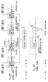
FIG. 12 shows an arrangement of the input section
in each separate multiplexing section of the tag-based
multiplexing device. The input section (hereinafter
termed the input section 60) receives a clock signal,
a cell frame signal, a cell enable signal, and cell
data from the adjacent upstream separate multiplexing
section over the upstream cascading line. The input
section 60 further receives a master/slave signal and
a input-lines indication signal from the general
control unit, not shown. An output signal of the
input section 60 consists of a clock signal, a cell
frame signal, a cell enable signal, cell data, an
input interruption detect signal, and a tag signal.
In FIG. 12, each of the clock detector 41, the cell
frame detector 42, the OR circuit 44, the cell frame
generator 45, and the selector 46, is the same as the
corresponding unit shown in FIG. 9.
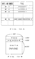
A tag information memory 61 stores, as shown in
FIG. 13A, pieces of 8-bit tag information in a
one-to-one correspondence relationship with input line
numbers. The tag information identifies each input
line connected to the multiplexing device.
A control cell generator 62 accesses the tag
information memory 61 in response to the input-line
indication signal and then generates tag information
using tag information retrieved from the tag
information memory 61. The input-line indication
signal, which is presented by the general control
unit, not shown, indicates which of the separate
multiplexing sections the input lines are connected
with. For example, if an input line is connected to
the separate multiplexing section 30-2, then the
control cell generator 62 accesses the tag information
memory 61 with "#2" as a key and retrieves "00000010"
as tag information from the memory 61, as shown in
FIG. 13A.
The control cell generator 62 generates a control
cell such as shown in FIG. 13B. Tag information
retrieved from the tag information memory 61 is added
at the beginning of the control cell. Information
stored in the header and payload of the control cell
is not specifically defined.
If, for example, input lines #1 to #N are
connected to the separate multiplexing sections 30-1
to 30-N, respectively, then the input-line indication
signal will take the form of "#1, #2, ..., #N". In
this case, the control cell generator 62 holds N
pieces of tag information that have been retrieved
from the tag information memory 61 with #1 to #N as
keys, and generates N types of control cells each of
which is headed by the corresponding tag information.
The control cells are outputted in a cyclical manner.
The output of the control cell generator 62 is
connected to an input of a selector 63, which has the
other input connected to receive cell data transferred
over the upstream cascading line.
Upon receipt of a master/slave signal at a high
level indicating master, the selector 63 selects a
control cell generated by the control cell generator
62. On the other hand, when the master/slave signal
is a 0 to indicate slave, the selector 63 selects cell
data transferred over the upstream cascading line.
That is, the most upstream separate multiplexing
section generates a control cell by itself, while the
other separate multiplexing sections each use a
control cell sent from the upstream side.
A tag information detector 64 receives an output
of the selector 63 to detect tag information added at
the beginning of a control cell. The result of
detection is presented to the controller 33. If, for
example, the tag detector 64 in the separate
multiplexing section 30-1 shown in FIG. 7 receives a
cell data stream as shown in FIG. 11A, it detects
"00000001" to "00000100" in sequence as tag
information corresponding to #1 to #4 and presents the
detected tag information in sequence to the controller
33.
Although, in the above arrangement, each of the
input sections 60 is equipped with a tag information
memory 61 and a control cell generator 62, the
arrangement may be modified such that a single tag
information memory and a single control cell generator
are provided for all the separate multiplexing
sections 30-1 to 30-N. In this case, an output of the
control cell generator is applied in common to each
of the selectors 63 of the input sections 60 of the
separate multiplexing sections 30-1 to 30-N.
The controller 33 in each of the separate
multiplexing sections 30-1 to 30-N of the tag-based
multiplexing device knows the identification number,
1, 2, ... or N, of the separate multiplexing section
to which it belongs. This number also identifies the
input line which is connected to the corresponding
separate multiplexing section. For example, "1" has
been set in advance as a line number in the controller
33 in the separate multiplexing section 30-1 to which
the input line #1 is connected. When receiving pieces
of tag information presented sequentially by the tag
information detector 64, the controller 33 compares
each of the line numbers specified by the pieces of
tag information in turn with the line number that has
been set in advance, as shown in FIG. 14. Only when
the comparison indicates equality, the controller 33
issues a read enable signal. The read enable signal
is used to read one cell out of the FIFO memory
connected to the input line. In this manner, the
controller 33 can recognize the timing of multiplexing
of a cell received over the input line by tag
information, to multiplex that cell on the cascading
line on a timely basis.
The tag-based multiplexing device described so far
in connection with FIGs. 11 to 14 is arranged such
that each of the separate multiplexing sections 30-1
to 30-N knows the timing of multiplexing by tag
information added at the beginning of a control cell
transferred over the cascading line. Alternatively,
the arrangement may be modified such that, as shown
in FIGs. 15A and 15B, data corresponding to tag
information and cell data are sent simultaneously, in
parallel, and each separate multiplexing section knows
the multiplexing timing by that data corresponding to
tag information.
As described above, the multiplexing device of the
present embodiment makes it a condition that the sum
of the bandwidths of the input lines #1 to #N is
basically equal to or less than the bandwidth of the
multiplexed output line 12. In other words, the
number of input lines and the bandwidth of each input
line can be determined with freedom, unless the sum
of the bandwidths of the input lines exceeds the
bandwidth of the multiplexed output line. The
multiplexing device of the present embodiment can
accommodate input lines having different bit rates
(bandwidths). The input lines #1 to #N that can be
accommodated assume their bit rates to be 150 Mbps,
45 Mbps, and 1.5 Mbps. Assuming, for example, that
the bit rate of the multiplexed output line 12 is 2.4
Gbps (the bandwidth is 2.4 GHz), 10 input lines that
run at a bit rate of 150 Mbps (bandwidth = 150 MHz)
and 10 input lines that run at a bit rate of 45 Mbps
(bandwidth = 45 MHz) can be accommodated under the
above condition. In this case, however, in the
arrangement shown in FIG. 7, there arises a
possibility that cells may be discarded because the
bandwidth of the multiplexed output line is equally
assigned to each of the input lines #1 to #N. That
is, when the bandwidth of the multiplexed output line
is equally assigned to 20 input lines, each input line
is assigned 120 MHz only. Under this situation, cells
that are received over an input line which runs at a
bit rate of 150 Mbps (a bandwidth of 150 MHz) will be
discarded.
To circumvent this problem, there are two possible
methods. The first method is to make a comparison
between the sum of the bandwidths of the input lines
#1 to #N and the bandwidth of the multiplexed output
line on the assumption that each input line has the
maximum bandwidth. In this case, even if input lines
of 150 Mbps and input lines of 45 Mbps are mixed, each
input line is considered to have a bit rate of 150
Mbps when making a decision as to whether the above
condition is met. It thus follows that the
multiplexing device can accommodate only 16 input
lines at most. The other method is to assign the
bandwidth of the multiplexed output line to the 20
input lines on a different basis depending on their
respective bandwidths (as opposed to on an equal
basis).
If the multiplexing device allows cells to be
discarded, there is no necessity that the sum of the
bandwidths of the input lines should be less than the
bandwidth of the multiplexed output line.
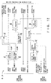
Next, a description is given of an arrangement
for, in the event of a failure in some of the separate
multiplexing sections 20-1 to 20-N or 30-1 to 30-N in
FIG. 5 or 7, reducing the effect of that failure on
the multiplexing device to a minimum.
FIG. 16 shows a multiplexing device that has a
function of reducing the effect of a failure. Here,
the separate multiplexing sections 20-1 to 20-N in
FIG. 5 or 30-1 to 30-N in FIG. 7 are simply
represented by separate multiplexing sections #1 to
#N.
In FIG. 16A, there are illustrated separate
multiplexing sections #1 to #4 as part of the separate
multiplexing device. These are connected in cascade
such that the separate multiplexing section #1 is the
most upstream one and the separate multiplexing
section #4 is the most downstream one among #1 - #4.
A general control unit 71 controls all the separate
multiplexing sections #1 to #N. That is, the general
control unit 71 supervises the status of each of the
separate multiplexing sections #1 to #N and, upon
detecting a failure, disconnects the separate
multiplexing section that is the source of the failure
from the multiplexing device, thereby protecting the
input lines associated with the other separate
multiplexing sections from the failure.
Assume, for example, that a failure has occurred
in the separate multiplexing section #2 as shown in
FIG. 16A. Then, the separate multiplexing section #3
will detect an abnormality in the clock or cell frame
signal (or the token in the system of FIG. 9) through
the cascading line. The abnormality is detected by
a failure monitor 22 shown in the arrangement of FIG.
5 or by the clock detector 41, the cell frame detector
42, and the token detector 43 in the arrangement of
FIG. 9 or FIG. 12. Upon detecting such an
abnormality, the separate multiplexing section #3
presents an input interruption detect signal to the
general control unit 71.
Upon receipt of the input interruption detect
signal from the separate multiplexing section #3, the
general control unit 71 considers a failure to have
occurred in the separate multiplexing section #2
immediately upstream of the separate multiplexing
section #3 and outputs a bypass instruction signal to
the separate multiplexing section #2. In response to
the bypass instruction signal, the separate
multiplexing section #2 passes data (cell and control
data) received over the upstream cascading line to the
downstream cascading line as they are. In this state,
cells received over other input lines than the input
line #2 will be multiplexed on the multiplexed output
line 12.
FIG. 16B shows an arrangement of a bypassing
facility provided for each separate multiplexing
section. In each separate multiplexing section, the
upstream cascading line is connected to main circuitry
72 and an input of a selector 73. In the arrangement
of FIG. 5, the main circuitry 72 comprises the FIFO
memories 21 and 23, the failure monitor 22, the
controller 24, and the selector 25. In the
arrangement of FIG. 7, the main circuitry 72 comprises
the FIFO memory 31, the input section 32, the
controller 33, and the selector 34. The output of the
main circuitry 72 is connected to the other input of
the selector 73. The output of the selector 73 is
connected to the downstream cascading line.
In the absence of a bypass instruction signal from
the general control unit 71, the selector 73 selects
the output of the main circuitry 72 to connect it to
the downstream cascading line. When receiving a
bypass instruction signal, on the other hand, the
selector 73 allows data received over the upstream
cascading line to be sent over the downstream
cascading line as they are. Thus, the failing
separate multiplexing section is bypassed.
In the event that failures have occurred in a
plurality of separate multiplexing sections, the
bypass processing is performed in the most upstream
one of the failing separate multiplexing sections.
When this bypass processing fails to restore the
multiplexing device to normal operation, an attempt
is made to perform the bypass processing in the
downstream multiplexing section next to that most
upstream one. If this attempt ends in failure, then
the bypass processing is performed in the further
adjacent downstream section.
When, in the above example, the separate
multiplexing section #2 is recovered from the failure
and hence the separate multiplexing section #3 ceases
outputting the input interruption detect signal, the
general control unit 71 resets the bypass instruction
signal, thereby returning the separate multiplexing
section #2 to the cascade connection.
FIG. 17 shows an arrangement of another example of
the multiplexing device having a function of reducing
the effect of a failure on the multiplexing
arrangement. In the arrangement of FIG. 17, a general
control unit 74 supervises the status of each separate
multiplexing section and, upon detecting a failure,
disconnects a separate multiplexing section which is
the source of the failure and its upstream separate
multiplexing sections from the multiplexing device,
thereby preventing the failure from affecting the
separate multiplexing sections downstream of that
failed separate multiplexing section.
Upon receipt of an input interruption detect
signal from the separate multiplexing section #3, the
general control unit 74 considers the separate
multiplexing section #2 immediately upstream of the
separate multiplexing section #3 to have failed and
then disconnects the failing separate multiplexing
section #2 and the separate multiplexing section #1
from the separate multiplexing device. That is, the
general control unit 74 sets the master/slave signal
presented to the separate multiplexing section #3 to
the master mode, thereby setting the separate
multiplexing section #3 as the most upstream separate
multiplexing section. In this state, incoming cells
received over the input lines 3, 4,.. will be
multiplexed.
When, in the above example, the separate
multiplexing section #2 is recovered from the failure
and hence the separate multiplexing section #3 ceases
outputting the input interruption detect signal, the
general control unit 74 sets the separate multiplexing
section #1 to the master mode and the separate
multiplexing section #3 to the slave mode, thereby
returning the separate multiplexing sections #1 and
#2 to the cascade connection.
The embodiments of the present invention have been
described in terms of an arrangement in which the
multiplexing device is installed on the input side of
the ATM switch. This is merely exemplary. The
present invention is applicable to all of arrangements
that multiplex cells received over a plurality of
input lines on a single output line.
In addition, the present invention can be applied
not only to an ATM system but also to systems that
transfer data in the form of fixed length packets.
Unlike the conventional MUX system, in the
arrangement in which input lines are connected in
cascade and each input line is multiplexed in turn,
there is no need for another multiplexing block (LSI
of FIG. 1C) in order to accommodate more input lines
than one multiplexing block can accommodate. Thus,
the multiplexing arrangement of the present invention
can flexibly adapt itself to any change in the number
of input lines. In addition, unlike the conventional
system, the multiplexing device of the invention
allows high-speed multiplexing processing to be
implemented because no WIRED-OR connection is used.
In the arrangement in which the bandwidth of the
multiplexed output line is assigned to the input lines
equally and periodically, each input line is
multiplexed equally.
In the event that a failure occurs in a separate
multiplexing section, only the failed separate
multiplexing section or both the failed separate
multiplexing section and its upstream separate
multiplexing section are disconnected from the
multiplexing device, allowing the effect of the
failure on the multiplexing device to be reduced to
a minimum.