EP0862213A2 - Semiconductor apparatus, circuit board and combination thereof - Google Patents
Semiconductor apparatus, circuit board and combination thereof Download PDFInfo
- Publication number
- EP0862213A2 EP0862213A2 EP98103510A EP98103510A EP0862213A2 EP 0862213 A2 EP0862213 A2 EP 0862213A2 EP 98103510 A EP98103510 A EP 98103510A EP 98103510 A EP98103510 A EP 98103510A EP 0862213 A2 EP0862213 A2 EP 0862213A2
- Authority
- EP
- European Patent Office
- Prior art keywords
- connection terminals
- connection
- semiconductor apparatus
- circuit board
- plane
- Prior art date
- Legal status (The legal status is an assumption and is not a legal conclusion. Google has not performed a legal analysis and makes no representation as to the accuracy of the status listed.)
- Granted
Links
Images




Classifications
-
- H—ELECTRICITY
- H05—ELECTRIC TECHNIQUES NOT OTHERWISE PROVIDED FOR
- H05K—PRINTED CIRCUITS; CASINGS OR CONSTRUCTIONAL DETAILS OF ELECTRIC APPARATUS; MANUFACTURE OF ASSEMBLAGES OF ELECTRICAL COMPONENTS
- H05K1/00—Printed circuits
- H05K1/02—Details
- H05K1/14—Structural association of two or more printed circuits
- H05K1/141—One or more single auxiliary printed circuits mounted on a main printed circuit, e.g. modules, adapters
-
- H—ELECTRICITY
- H10—SEMICONDUCTOR DEVICES; ELECTRIC SOLID-STATE DEVICES NOT OTHERWISE PROVIDED FOR
- H10W—GENERIC PACKAGES, INTERCONNECTIONS, CONNECTORS OR OTHER CONSTRUCTIONAL DETAILS OF DEVICES COVERED BY CLASS H10
- H10W72/00—Interconnections or connectors in packages
-
- H—ELECTRICITY
- H05—ELECTRIC TECHNIQUES NOT OTHERWISE PROVIDED FOR
- H05K—PRINTED CIRCUITS; CASINGS OR CONSTRUCTIONAL DETAILS OF ELECTRIC APPARATUS; MANUFACTURE OF ASSEMBLAGES OF ELECTRICAL COMPONENTS
- H05K1/00—Printed circuits
- H05K1/18—Printed circuits structurally associated with non-printed electric components
- H05K1/182—Printed circuits structurally associated with non-printed electric components associated with components mounted in printed circuit boards [PCB], e.g. insert-mounted components [IMC]
- H05K1/183—Printed circuits structurally associated with non-printed electric components associated with components mounted in printed circuit boards [PCB], e.g. insert-mounted components [IMC] associated with components mounted in and supported by recessed areas of the PCBs
-
- H—ELECTRICITY
- H10—SEMICONDUCTOR DEVICES; ELECTRIC SOLID-STATE DEVICES NOT OTHERWISE PROVIDED FOR
- H10W—GENERIC PACKAGES, INTERCONNECTIONS, CONNECTORS OR OTHER CONSTRUCTIONAL DETAILS OF DEVICES COVERED BY CLASS H10
- H10W70/00—Package substrates; Interposers; Redistribution layers [RDL]
- H10W70/40—Leadframes
- H10W70/421—Shapes or dispositions
- H10W70/424—Cross-sectional shapes
- H10W70/427—Bent parts
- H10W70/429—Bent parts being the outer leads
-
- H—ELECTRICITY
- H10—SEMICONDUCTOR DEVICES; ELECTRIC SOLID-STATE DEVICES NOT OTHERWISE PROVIDED FOR
- H10W—GENERIC PACKAGES, INTERCONNECTIONS, CONNECTORS OR OTHER CONSTRUCTIONAL DETAILS OF DEVICES COVERED BY CLASS H10
- H10W70/00—Package substrates; Interposers; Redistribution layers [RDL]
- H10W70/60—Insulating or insulated package substrates; Interposers; Redistribution layers
- H10W70/62—Insulating or insulated package substrates; Interposers; Redistribution layers characterised by their interconnections
- H10W70/65—Shapes or dispositions of interconnections
- H10W70/657—Shapes or dispositions of interconnections on sidewalls or bottom surfaces of the package substrates, interposers or redistribution layers
-
- H—ELECTRICITY
- H10—SEMICONDUCTOR DEVICES; ELECTRIC SOLID-STATE DEVICES NOT OTHERWISE PROVIDED FOR
- H10W—GENERIC PACKAGES, INTERCONNECTIONS, CONNECTORS OR OTHER CONSTRUCTIONAL DETAILS OF DEVICES COVERED BY CLASS H10
- H10W74/00—Encapsulations, e.g. protective coatings
- H10W74/10—Encapsulations, e.g. protective coatings characterised by their shape or disposition
- H10W74/111—Encapsulations, e.g. protective coatings characterised by their shape or disposition the semiconductor body being completely enclosed
- H10W74/114—Encapsulations, e.g. protective coatings characterised by their shape or disposition the semiconductor body being completely enclosed by a substrate and the encapsulations
- H10W74/117—Encapsulations, e.g. protective coatings characterised by their shape or disposition the semiconductor body being completely enclosed by a substrate and the encapsulations the substrate having spherical bumps for external connection
-
- H—ELECTRICITY
- H10—SEMICONDUCTOR DEVICES; ELECTRIC SOLID-STATE DEVICES NOT OTHERWISE PROVIDED FOR
- H10W—GENERIC PACKAGES, INTERCONNECTIONS, CONNECTORS OR OTHER CONSTRUCTIONAL DETAILS OF DEVICES COVERED BY CLASS H10
- H10W78/00—Detachable holders for supporting packaged chips in operation
-
- H—ELECTRICITY
- H10—SEMICONDUCTOR DEVICES; ELECTRIC SOLID-STATE DEVICES NOT OTHERWISE PROVIDED FOR
- H10W—GENERIC PACKAGES, INTERCONNECTIONS, CONNECTORS OR OTHER CONSTRUCTIONAL DETAILS OF DEVICES COVERED BY CLASS H10
- H10W90/00—Package configurations
- H10W90/701—Package configurations characterised by the relative positions of pads or connectors relative to package parts
-
- H—ELECTRICITY
- H05—ELECTRIC TECHNIQUES NOT OTHERWISE PROVIDED FOR
- H05K—PRINTED CIRCUITS; CASINGS OR CONSTRUCTIONAL DETAILS OF ELECTRIC APPARATUS; MANUFACTURE OF ASSEMBLAGES OF ELECTRICAL COMPONENTS
- H05K1/00—Printed circuits
- H05K1/02—Details
- H05K1/14—Structural association of two or more printed circuits
- H05K1/145—Arrangements wherein electric components are disposed between and simultaneously connected to two planar printed circuit boards, e.g. Cordwood modules
-
- H—ELECTRICITY
- H05—ELECTRIC TECHNIQUES NOT OTHERWISE PROVIDED FOR
- H05K—PRINTED CIRCUITS; CASINGS OR CONSTRUCTIONAL DETAILS OF ELECTRIC APPARATUS; MANUFACTURE OF ASSEMBLAGES OF ELECTRICAL COMPONENTS
- H05K2201/00—Indexing scheme relating to printed circuits covered by H05K1/00
- H05K2201/04—Assemblies of printed circuits
- H05K2201/049—PCB for one component, e.g. for mounting onto mother PCB
-
- H—ELECTRICITY
- H05—ELECTRIC TECHNIQUES NOT OTHERWISE PROVIDED FOR
- H05K—PRINTED CIRCUITS; CASINGS OR CONSTRUCTIONAL DETAILS OF ELECTRIC APPARATUS; MANUFACTURE OF ASSEMBLAGES OF ELECTRICAL COMPONENTS
- H05K2201/00—Indexing scheme relating to printed circuits covered by H05K1/00
- H05K2201/10—Details of components or other objects attached to or integrated in a printed circuit board
- H05K2201/10613—Details of electrical connections of non-printed components, e.g. special leads
- H05K2201/10621—Components characterised by their electrical contacts
- H05K2201/10689—Leaded Integrated Circuit [IC] package, e.g. dual-in-line [DIL]
-
- H—ELECTRICITY
- H05—ELECTRIC TECHNIQUES NOT OTHERWISE PROVIDED FOR
- H05K—PRINTED CIRCUITS; CASINGS OR CONSTRUCTIONAL DETAILS OF ELECTRIC APPARATUS; MANUFACTURE OF ASSEMBLAGES OF ELECTRICAL COMPONENTS
- H05K2201/00—Indexing scheme relating to printed circuits covered by H05K1/00
- H05K2201/10—Details of components or other objects attached to or integrated in a printed circuit board
- H05K2201/10613—Details of electrical connections of non-printed components, e.g. special leads
- H05K2201/10621—Components characterised by their electrical contacts
- H05K2201/10734—Ball grid array [BGA]; Bump grid array
Definitions
- the present invention relates to a semiconductor apparatus, and more particularly to a package design and mounting technique of a semiconductor apparatus.
- semiconductor chips are incorporated into an individual protective package, connected onto a printed circuit board.
- external terminals (connection terminals) extending from the protective package are bonded onto a flat plane of the printed circuit board.
- leads (connection terminals) are bonded around the package onto the surface of the printed circuit board.
- the pitch (spacing) between two adjacent leads is designed to be small, such as 1.27 mm, so as to contribute increasing the number of leads (terminals).
- Such a package is designed small in size and is shaped almost square, so that connecting lines (inner leads) in the package can be designed to have the same length; and therefore, it is easy to control impedance thereof.
- Such package design is useful for a high performance semiconductor apparatus.
- connection terminals are connected onto the single plane of the printed circuit board, so that it is required to narrow the pitch between two adjacent terminals in order to increase the number of terminals.
- the pitch of the connection terminals is basically defined by the mounting technique, for example, 0.3 mm of pitch would be the minimum for QFP in reflow solder-bonding technique. Accordingly, in order to increase the number of the connection terminals, it is the only way to make a pitch of terminals narrower than 0.3 mm. According to the current mounting technology, however, it is difficult to mount the semiconductor apparatus, having the connection terminals with a pitch of less than 0.3 mm, onto the printed circuit board.
- an object of the invention is to provide a semiconductor apparatus which can be easily mounted onto a circuit board even though connection terminals are increased in number.
- Another object of the invention is to provide a circuit board that contributes to increase the number of connection terminals. of a semiconductor apparatus.
- a semiconductor apparatus includes a semiconductor chip contained in a package; a first set of connection terminals, of which one ends are connected to the semiconductor chip and the other ends are connected onto a first connection plane outside of the package; and a second set of connection terminals, of which one ends are connected to the semiconductor chip and the other ends are connected onto a second connection plane outside of the package.
- the first and second connection planes are electrically connected to a circuit board.
- the first and second sets of connection terminals may be arranged alternately with a predetermined pitch in the package.
- a circuit board onto which a semiconductor apparatus is mounted includes a first connection plane onto which one ends of a first set of connection terminals, extending from the semiconductor apparatus, are connected; and a second connection plane onto which one ends of a second set of connection terminals, extending from the semiconductor apparatus, are connected.
- the first and second connection planes may be arranged perpendicularly to each other.
- the first set of connection terminals extend to the first connection plane, while the second set of connection terminals extend to the second connection plane.
- the first and second connection planes may be arranged parallel to each other in the different levels. In this case, the first set of connection terminals extend to the first connection plane, and the second set of connection terminals extend parallel to the second connection plane.
- a third aspect of the invention is provided on a combination of the above described semiconductor apparatus and circuit board.
- the first and second sets of connection terminals are connected to the different planes, so that the number of connection terminals can be easily increased without narrowing the pitch of the terminals on the circuit board.
- the connection terminals can be arranged with enough spacing outside the package.
- Fig. 1 is a side view illustrating a conventional semiconductor apparatus.
- Fig. 2 is a side view illustrating a conventional semiconductor apparatus.
- Fig. 3 is a side view illustrating a conventional semiconductor apparatus.
- Fig. 4 is a side view illustrating a conventional semiconductor apparatus mounted directly onto a printed circuit board.
- Fig. 5 is a side view illustrating a conventional semiconductor apparatus mounted directly onto a printed circuit board.
- Fig. 6 is a side view illustrating a conventional semiconductor apparatus mounted to a printed circuit board with insert-mounting technique.
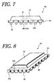
- Fig. 7 is a side view illustrating a semiconductor apparatus according to a first preferred embodiment of the invention.
- Fig. 8 is a perspective view illustrating the semiconductor apparatus, shown in Fig. 7.
- Fig. 9 is a side view illustrating the semiconductor apparatus, shown in Figs. 7 and 8, mounted directly onto a printed circuit board.
- Fig. 10 is a side view illustrating the semiconductor apparatus, shown in Figs. 7 and 8, mounted to a printed circuit board.
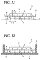
- Fig. 11 is a side view illustrating a semiconductor apparatus according to a second preferred embodiment of the invention.
- Fig. 12 is a side view illustrating the semiconductor apparatus, shown in Fig. 11, mounted directly onto a printed circuit board.
- Fig. 13 is a side view illustrating a semiconductor apparatus according to a second preferred embodiment of the invention.
- Fig. 14 is a side view illustrating the semiconductor apparatus, shown in Fig. 13, mounted directly onto a printed circuit board.
- Fig. 1 shows a typical conventional package, that is QFP (Quad Flat Package), QFJ (Quad Flat J-Lead), SOJ (Small Outline J-Lead) or the like.
- leads (connection terminals) 12 are arranged with a pitch of 0.8 mm and extend from a resin-molded package 10 outwardly.
- a semiconductor chip, not shown, is contained in the resin-molded packaged 10.
- a lead pitch (spacing) has been got narrower in the order of 1.0 mm, 0.8 mm, 0.65 mm, 0.5 mm, 0.4 mm to 0.3mm, as shown in Figs. 2 and 3.
- leads (connection terminals) 16 are arranged with a pitch of 0.65 mm and extend from a resin-molded package 14 outwardly.
- leads (connection terminals) 20 are arranged with a pitch of 0.50 mm and extend from a resin-molded package 18 outwardly.
- Fig. 4 shows a conventional semiconductor apparatus 22 mounted onto a surface of a printed circuit board 26 using surface mounting technique. Each ends of leads 24 are electrically connected onto the printed circuit board 26.
- Fig. 5 shows a conventional semiconductor apparatus 28 mounted onto a surface of a printed circuit board 26 using surface mounting technique.
- the semiconductor apparatus (package) 28 is of BGA (Ball Grid Array) type.
- Fig. 6 shows a conventional semiconductor apparatus 32 mounted onto a surface of a printed circuit board 36 using insert mounting technique. leads 34, extending from the package (32) are inserted into through-holes of the printed circuit board 36.
- the leads are connected onto the single plane of circuit board, so that it is required to narrow the pitch between two adjacent leads in order to increase the number of leads. Accordingly, in order to increase leads, it is the only way to make a pitch of leads narrower than 0.3 mm. According to the current mounting technology, however, it is difficult to mount the semiconductor apparatus, having leads with a pitch of less than 0.3 mm, onto a circuit board.
- Figs. 7 and 8 show a semiconductor apparatus 40, according to a first preferred embodiment of the invention.
- the semiconductor apparatus 40 includes a semiconductor chip 41, a resin package 42 protecting the semiconductor chip 41, and a resin substrate 44.
- the resin substrate 44 is shaped to have a bottom surface (first connection plane) 44a and a side surface with depressed portions (second connection plane) 44b.
- a first set of connection terminals 46 are attached on the bottom surface 44a of the resin substrate 44.
- a second set of connection terminals 48 are attached on the depressed portions 44b (second connection plane) of the resin substrate 44.
- the first and second sets of connection terminals 46 and 48 are arranged alternately to each other.
- the first set of connection terminals 46 are arranged with a predetermined pitch to have an enough spacing between two adjacent terminals.
- the first and second sets of connection terminals 46 and 48 are arranged on the different planes 44a and 44b, so that the first and second sets of connection terminals 46 and 48 are completely insulated from each other. As a result, the different signals are transmitted through the first and second sets of connection terminals 46 and 48.
- the semiconductor apparatus 40 can be fabricated by conventional technique.
- Fig. 9 shows the semiconductor apparatus 40 mounted directly onto first and second printed-circuit boards 50 and 52. Having two different planes of circuit boards is one feature of the invention.
- the first printed-circuit board 50 is designed to have a horizontal upper surface.
- the second printed-circuit board 52 is arranged perpendicularly to the first printed-circuit board 50.
- the first and second printed-circuit board 50 and 52 are provided with wiring patterns (not shown) at locations corresponding to the first and second connection terminals 46 and 48.
- the semiconductor apparatus 40 is first placed on the first printed-circuit board 50, then the first set of connection terminals 46 are electrically connected with adhesive material onto the wiring pattern of the first printed-circuit board 50.
- the second set of connection terminals 48 are electrically connected with the adhesive material 54 onto the wiring pattern of the second printed-circuit board 52.
- the second set of connection terminals 48 are provided on the depressed plane 44b (second connection plane) of the resin substrate 44, and are electrically connected to the wiring pattern of the second printed-circuit board 52.
- the adhesive material 54 is partially inserted into the second set of connection terminals 48 that is shaped to be concave.
- Fig. 10 shows the semiconductor apparatus 40 mounted onto a printed-circuit board 60 using a socket 58.
- contact pins 62 and 64 are connected to the first and second sets of connection terminals 46 and 48, respectively.
- the contact pins 62 and 64 extend out of the socket 58 to function as external pins.
- the contact pins 62 are arranged to face the first set of connection terminals 46 of the semiconductor apparatus 40, and the contact pins 64 are arranged to face the second set of connection terminals 48.
- the contact pins 62 are shaped to have flat tops 62a to be in contact with the first set of connection terminals 46, and the contact pins 64 are shaped to have guide portions 64a to be in contact with the second set of connection terminals 48.
- the socket 58 is connected through the contact pins 62 and 64 to the printed-circuit board 60 in advance.
- the semiconductor apparatus 40 is mounted into the socket 58, then the first set of connection terminals 46 are electrically connected to the contact pins 62 with adhesive material, and the second set of connection terminals 48 are electrically connected to the contact pins 64 with adhesive material 54.
- the adhesive material 54 may be in advance put onto the first and second sets of connection terminals 46 and 48, then the semiconductor apparatus 40 with the adhesive material 54 may be placed into the socket 58.
- the first set of connection terminals 46 are arranged at the bottom surface (projected plane) 44a of the resin substrate 44, and the second set of connection terminals 48 are arranged on the second plane 44b, so that the semiconductor apparatus 40 can be provided with many terminals arranged with a narrow pitch.
- connection terminals 46 and 48 are connected to the different planes 50 and 52 (62a and 64a), so that the connection terminals 46 and 48 can be completely insulated from each other. Therefore, the pitch of the connection terminals in the package 42 can be narrowed and more terminals can be used for the semiconductor apparatus.
- the first and second sets of connection terminals 46 and 48 are connected to the different planes 44a and 44b, so that the number of connection terminals 46 and 48 can be easily increased without narrowing the pitch of the terminals on the circuit board 50 (60). In other words, even if the connection terminals 46 and 48 are tightly arranged in the package 42, the connection terminals 46 and 48 can be arranged with enough spacing outside the package 42.
- Fig. 11 shows a semiconductor apparatus 70 according to a second preferred embodiment of the invention.
- Fig. 12 shows the semiconductor apparatus 70 mounted onto first and second printed-circuit board 78 and 79.
- the semiconductor apparatus 70 includes a resin package 72 containing a semiconductor chip, not shown, a first set of connection terminals (leads) 74, and a second set of connection terminals (leads) 76.
- the first and second sets of connection terminals 74 and 76 extend from the package 72 toward a first plane A and a second plane B, respectively.
- the first and second sets of connection terminals 74 and 76 are arranged alternately to each other.
- the second plane B is arranged to be perpendicular to the plane A.
- One ends of the first set of connection terminals 74 are connected to the semiconductor chip in the resin packaged 72, and the other ends are perpendicularly bent to increase the area being in contact with the first plane A.
- One ends of the second set of connection terminals 76 are connected to the semiconductor chip in the resin packaged 72, and the other ends are perpendicularly bent to increase the area being in contact with the second plane B.
- the pitch of each set of terminals is designed to be 0.5 mm, the two adjacent terminals would have a spacing (pitch) of 0.25 mm in the resin package 72.
- the semiconductor apparatus 70 is mounted to first and second printed-circuit boards 78 and 79.
- the first and second printed-circuit boards 78 and 79 are provided with wiring patterns (not shown) at locations corresponding to the connection terminals 74 and 76.
- the semiconductor apparatus 70 is placed on the first printed-circuit board 78, then the first set of connection terminals 74 are electrically connected with adhesive material onto the wiring pattern of the first printed-circuit board 78.
- the second set of connection terminals 76 are electrically connected with the adhesive material onto the wiring pattern of the second printed-circuit board 79.
- the first and second printed-circuit boards 78 and 79 correspond to the first and second planes A and B, in Fig. 11.
- Fig. 13 shows a semiconductor apparatus 80 according to a third preferred embodiment of the invention.
- Fig. 14 shows the semiconductor apparatus 80 mounted directly onto first and second printed-circuit boards 88 and 89.
- the semiconductor apparatus 80 includes a resin package 82 containing a semiconductor chip (not shown); a first set of connection terminals (leads) 84 extending from the resin package 82 toward a lower plane A (first plane); and a second set of connection terminals 86 extending from the resin package 82 parallel to a plane C (second plane).
- the first and second sets of connection terminals 84 and 86 are arranged alternately to each other.
- connection terminals 84 are shaped to have perpendicularly-bent ends to increase the area to be in contact with the plane A.
- the plane C is arranged perpendicular to the plane A.
- the second set of connection terminals 86 are in contact with the plane C without spacing between them.
- the pitch of each connection terminals 84 and 86 is designed to be 0.5 mm, the two adjacent terminals would have a spacing (pitch) of 0.25 mm in the resin package 82.
- the first and second printed-circuit boards 88 and 89 correspond to the first and second planes A and C, respectively.
- the first and second planes A and C are arranged parallel to each other.
- the first and second printed-circuit boards 88 and 89 are provided with wiring patterns (not shown) at locations corresponding to the connection terminals 84 and 86.
- the semiconductor apparatus 80 is first placed on the first printed-circuit board 88, then the first set of connection terminals 84 are electrically connected with adhesive material onto the wiring pattern of the printed-circuit board 88. Next, the second set of connection terminals 86 are electrically connected with the adhesive material onto the wiring pattern of the second printed-circuit board 89.
- the semiconductor apparatus 80 even if the pitch of the first and second set of connection terminals 84 and 86 is designed to be 0.25 mm in the resin packaged 82, the two adjacent terminals to he connected onto the printed-circuit boards 88 and 89 would have a spacing (pitch) of 0.5 mm. Therefore, the semiconductor apparatus 80 is easily mounted onto the circuit boards 88 and 89.
- the first and second printed-circuit boards 88 and 89 are arranged parallel to each other, so that the total thickness can be reduced.
- the first and second sets of connection terminals are connected to the different planes, so that the number of connection terminals can be easily increased without narrowing the pitch of the terminals on the circuit board.
- the connection terminals can be arranged with enough spacing outside the package.
- the invention is applicable to any types of semiconductor apparatuses and any types of packages. It is clear that the pitch of the connection terminals is not limited by the above described embodiments. Fabrication process, the type of the chip substrate, the number of terminals, the arrangement of the package, and so on are not limited by above described embodiments.
Landscapes
- Engineering & Computer Science (AREA)
- Microelectronics & Electronic Packaging (AREA)
- Lead Frames For Integrated Circuits (AREA)
- Wire Bonding (AREA)
- Combinations Of Printed Boards (AREA)
Abstract
Description
Claims (21)
- A semiconductor apparatus, having a package containing a semiconductor chip inside, comprising:a first set of connection terminals, of which one ends are connected to the semiconductor chip and the other ends are connected onto a first connection plane outside of the package; anda second set of connection terminals, of which one ends are connected to the semiconductor chip and the other ends are connected onto a second connection plane outside of the package, wherein
the first and second connection planes are electrically connected to a circuit board. - The semiconductor apparatus, according to claim 1, wherein
the first and second sets of connection terminals are arranged alternately with a predetermined pitch in the package. - The semiconductor apparatus, according to claim 1, wherein:
the first connection terminals are arranged on a first surface of the package, while the second connection terminals are arranged on a second surface of the package. - The semiconductor apparatus, according to claim 3, wherein
the first and second surfaces are perpendicularly to each other. - The semiconductor apparatus, according to claim 4, further comprising:an insulation substrate, wherein
the first set of connection terminals are arranged at a bottom surface of the insulation substrate, while the second set of connection terminals are arranged at a side surface of the insulation substrate. - The semiconductor apparatus, according to claim 5, wherein
the semiconductor apparatus is of BGA (Ball Grid Array) type. - The semiconductor apparatus, according to claim 6, wherein
the first set of connection terminals are connected to first contact pins,
the second set of connection terminals are connected to second contact pins, and
the first and second contact pins extend in the same direction to be connected to the circuit board. - The semiconductor apparatus, according to claim 7, wherein
the semiconductor apparatus is covered with a protection socket. - The semiconductor apparatus, according to claim 1, wherein
the first and second sets of connection terminals are arranged on a common surface, but are extending in the different directions from each other. - The semiconductor apparatus, according to claim 9, wherein
the first and second connection planes are arranged perpendicularly to each other, and
the first set of connection terminals extend to the first connection plane, while the second set of connection terminals extend to the second connection plane. - The semiconductor apparatus, according to claim 9, wherein
the first and second connection planes are arranged parallel to each other in the different levels, and
the first set of connection terminals extend to the first connection plane, and the second set of connection terminals extend parallel to the second connection plane. - A circuit board onto which a semiconductor apparatus is mounted, comprising:a first connection plane onto which one ends of a first set of connection terminals, extending from the semiconductor apparatus, are connected; anda second connection plane onto which one ends of a second set of connection terminals, extending from the semiconductor apparatus, are connected.
- The circuit board, according to claim 12, wherein
the first and second connection planes are arranged perpendicularly to each other. - The circuit board, according to claim 12, wherein
the first and second connection planes are arranged parallel to each other in the different levels. - A combination of a semiconductor apparatus and a circuit board, wherein,
the semiconductor apparatus having a package containing a semiconductor chip inside comprises:the circuit board comprises:(1) a first set of connection terminals, of which one ends are connected to the semiconductor chip; and(2) a second set of connection terminals, of which one ends are connected to the semiconductor chip, and(1) a first connection plane onto which the other ends of the first set of connection terminals are connected; and(2) a second connection plane onto which the other ends of the second set of connection terminals are connected. - The combination, according to claim 15, wherein
the first and second sets of connection terminals are arranged alternately with a predetermined pitch. - The combination, according to claim 15, wherein
the first and second connection terminals of the semiconductor apparatus are respectively arranged on first and second surfaces, which are perpendicularly to each other. - The combination, according to claim 17, wherein
the semiconductor apparatus further comprises an insulation substrate, of which a bottom surface and a side surface are arranged respectively parallel to the first and second connection planes of the circuit board, and
the first and second set of connection terminals are positioned on the bottom surface and side surface of the insulation substrate, respectively. - The combination, according to claim 15, wherein
the first and second connection terminals of the semiconductor apparatus are arranged on a common surface in the package, but are extending in the different directions. - The combination, according to claim 19, wherein
the first and second connection planes of the circuit board are arranged perpendicularly to each other, and
the first set of connection terminals extend to the first connection plane, while the second set of connection terminals extend to the second connection plane. - The combination, according to claim 19, wherein
the first and second connection planes of the circuit board are arranged parallel to each other in the different levels, and
the first set of connection terminals extend to the first connection plane, and the second set of connection terminals extend parallel to the second connection plane.
Applications Claiming Priority (3)
| Application Number | Priority Date | Filing Date | Title |
|---|---|---|---|
| JP9042775A JPH10242374A (en) | 1997-02-27 | 1997-02-27 | Semiconductor device |
| JP4277597 | 1997-02-27 | ||
| JP42775/97 | 1997-02-27 |
Publications (3)
| Publication Number | Publication Date |
|---|---|
| EP0862213A2 true EP0862213A2 (en) | 1998-09-02 |
| EP0862213A3 EP0862213A3 (en) | 1999-09-22 |
| EP0862213B1 EP0862213B1 (en) | 2004-05-06 |
Family
ID=12645353
Family Applications (1)
| Application Number | Title | Priority Date | Filing Date |
|---|---|---|---|
| EP98103510A Expired - Lifetime EP0862213B1 (en) | 1997-02-27 | 1998-02-27 | Semiconductor apparatus, circuit board and combination thereof |
Country Status (6)
| Country | Link |
|---|---|
| US (1) | US6054757A (en) |
| EP (1) | EP0862213B1 (en) |
| JP (1) | JPH10242374A (en) |
| KR (1) | KR100407751B1 (en) |
| DE (1) | DE69823574T2 (en) |
| TW (1) | TW373312B (en) |
Cited By (5)
| Publication number | Priority date | Publication date | Assignee | Title |
|---|---|---|---|---|
| EP1157967A2 (en) * | 2000-05-22 | 2001-11-28 | Lucent Technologies Inc. | Packaging micromechanical devices |
| GB2364435A (en) * | 1999-12-24 | 2002-01-23 | Nec Corp | Surface-mount package |
| WO2003103045A1 (en) * | 2002-05-29 | 2003-12-11 | Intel Corporation | High-power land grid array package and socket |
| ITVI20120145A1 (en) * | 2012-06-15 | 2013-12-16 | St Microelectronics Srl | COMPREHENSIVE STRUCTURE OF ENCLOSURE INCLUDING SIDE CONNECTIONS |
| EP2447993A4 (en) * | 2009-08-21 | 2014-10-01 | Huawei Device Co Ltd | ELECTRONIC MODULE AND METHOD OF PUSHING THE SAME |
Families Citing this family (7)
| Publication number | Priority date | Publication date | Assignee | Title |
|---|---|---|---|---|
| US6188230B1 (en) * | 1997-12-16 | 2001-02-13 | Intel Corporation | Pickup chuck for double sided contact |
| US7893545B2 (en) * | 2007-07-18 | 2011-02-22 | Infineon Technologies Ag | Semiconductor device |
| TWI405313B (en) * | 2010-03-31 | 2013-08-11 | Quanta Comp Inc | Integrated circuit package component with lateral conducting pins |
| JP2012069764A (en) | 2010-09-24 | 2012-04-05 | On Semiconductor Trading Ltd | Circuit device and method for manufacturing the same |
| US11862736B2 (en) | 2018-09-17 | 2024-01-02 | GBT Tokenize Corp. | Multi-dimensional photonic integrated circuits and memory structure having optical components mounted on multiple planes of a multi-dimensional package |
| US10854763B2 (en) | 2018-09-17 | 2020-12-01 | Gbt Technologies Inc. | Multi-dimensional integrated circuit having multiple planes and memory architecture having a honeycomb or bee hive structure |
| US11809797B1 (en) | 2022-07-31 | 2023-11-07 | Gbt Technologies Inc. | Systems and methods of predictive manufacturing of three-dimensional, multi-planar semiconductors |
Family Cites Families (11)
| Publication number | Priority date | Publication date | Assignee | Title |
|---|---|---|---|---|
| JPS582054A (en) * | 1981-06-26 | 1983-01-07 | Fujitsu Ltd | Semiconductor device |
| JPS5963751A (en) * | 1982-10-04 | 1984-04-11 | Matsushita Electronics Corp | Semiconductor device |
| FR2538961B1 (en) * | 1982-12-30 | 1985-07-12 | Europ Composants Electron | BASE FOR INTEGRATED CIRCUIT |
| JP2592308B2 (en) * | 1988-09-30 | 1997-03-19 | 株式会社日立製作所 | Semiconductor package and computer using the same |
| JPH04184967A (en) * | 1990-11-19 | 1992-07-01 | Mitsubishi Electric Corp | Semiconductor device |
| US5157480A (en) * | 1991-02-06 | 1992-10-20 | Motorola, Inc. | Semiconductor device having dual electrical contact sites |
| JPH05102262A (en) * | 1991-10-03 | 1993-04-23 | Hitachi Ltd | Semiconductor device and mounting device mounting the same |
| KR940022803A (en) * | 1993-03-05 | 1994-10-21 | 김광호 | Printed circuit board suitable for semiconductor package and its mounting |
| JPH0757832A (en) * | 1993-08-19 | 1995-03-03 | Fujitsu Ltd | Printed board connection structure |
| US5563446A (en) * | 1994-01-25 | 1996-10-08 | Lsi Logic Corporation | Surface mount peripheral leaded and ball grid array package |
| JP3825475B2 (en) * | 1995-06-30 | 2006-09-27 | 株式会社 東芝 | Manufacturing method of electronic parts |
-
1997
- 1997-02-27 JP JP9042775A patent/JPH10242374A/en active Pending
-
1998
- 1998-02-18 KR KR10-1998-0005012A patent/KR100407751B1/en not_active Expired - Fee Related
- 1998-02-24 TW TW087102604A patent/TW373312B/en not_active IP Right Cessation
- 1998-02-26 US US09/030,924 patent/US6054757A/en not_active Expired - Fee Related
- 1998-02-27 DE DE69823574T patent/DE69823574T2/en not_active Expired - Lifetime
- 1998-02-27 EP EP98103510A patent/EP0862213B1/en not_active Expired - Lifetime
Cited By (13)
| Publication number | Priority date | Publication date | Assignee | Title |
|---|---|---|---|---|
| US6756666B2 (en) | 1999-12-24 | 2004-06-29 | Nec Corporation | Surface mount package including terminal on its side |
| GB2364435A (en) * | 1999-12-24 | 2002-01-23 | Nec Corp | Surface-mount package |
| GB2364435B (en) * | 1999-12-24 | 2002-11-20 | Nec Corp | Surface-mount package with side terminal |
| EP1157967A2 (en) * | 2000-05-22 | 2001-11-28 | Lucent Technologies Inc. | Packaging micromechanical devices |
| US7402182B2 (en) | 2002-05-29 | 2008-07-22 | Intel Corporation | High-power LGA socket |
| US6870251B2 (en) | 2002-05-29 | 2005-03-22 | Intel Corporation | High-power LGA socket |
| WO2003103045A1 (en) * | 2002-05-29 | 2003-12-11 | Intel Corporation | High-power land grid array package and socket |
| CN100449746C (en) * | 2002-05-29 | 2009-01-07 | 英特尔公司 | Package and socket of semiconductor device and connection method of package and socket |
| EP2447993A4 (en) * | 2009-08-21 | 2014-10-01 | Huawei Device Co Ltd | ELECTRONIC MODULE AND METHOD OF PUSHING THE SAME |
| ITVI20120145A1 (en) * | 2012-06-15 | 2013-12-16 | St Microelectronics Srl | COMPREHENSIVE STRUCTURE OF ENCLOSURE INCLUDING SIDE CONNECTIONS |
| US9099453B2 (en) | 2012-06-15 | 2015-08-04 | Stmicroelectronics S.R.L. | Methods, circuits and systems for a package structure having wireless lateral connections |
| US9922945B2 (en) | 2012-06-15 | 2018-03-20 | Stmicroelectronics S.R.L. | Methods, circuits and systems for a package structure having wireless lateral connections |
| US10497655B2 (en) | 2012-06-15 | 2019-12-03 | Stmicroelectronics S.R.L. | Methods, circuits and systems for a package structure having wireless lateral connections |
Also Published As
| Publication number | Publication date |
|---|---|
| DE69823574D1 (en) | 2004-06-09 |
| KR19980071478A (en) | 1998-10-26 |
| KR100407751B1 (en) | 2004-03-20 |
| EP0862213B1 (en) | 2004-05-06 |
| DE69823574T2 (en) | 2005-04-28 |
| TW373312B (en) | 1999-11-01 |
| US6054757A (en) | 2000-04-25 |
| JPH10242374A (en) | 1998-09-11 |
| EP0862213A3 (en) | 1999-09-22 |
Similar Documents
| Publication | Publication Date | Title |
|---|---|---|
| US6118174A (en) | Bottom lead frame and bottom lead semiconductor package using the same | |
| US5153379A (en) | Shielded low-profile electronic component assembly | |
| US5600178A (en) | Semiconductor package having interdigitated leads | |
| US4463217A (en) | Plastic surface mounted high pinout integrated circuit package | |
| EP0729180A2 (en) | Packaging multi-chip modules without wirebond interconnection | |
| US7199478B2 (en) | Printed circuit board having an improved land structure | |
| US6054757A (en) | Semiconductor apparatus, circuit board and combination thereof | |
| JPH1050877A (en) | Semiconductor package | |
| JP2568748B2 (en) | Semiconductor device | |
| EP0587294B1 (en) | Semiconductor package | |
| US5330359A (en) | Socket for stacking integrated circuit chips | |
| US5324985A (en) | Packaged semiconductor device | |
| US5444299A (en) | Electronic package with lead wire connections | |
| KR19980070133A (en) | Semiconductor device, mounting apparatus of semiconductor device, and manufacturing method of semiconductor device | |
| KR100379083B1 (en) | Lead-on Chip Area Arrayed Semiconductor Package | |
| KR100342812B1 (en) | Area array bumped semiconductor package having ground and power lines | |
| KR100196992B1 (en) | Lead frame and chip scale package having it | |
| KR19980039676A (en) | Easy to mount bottom lead package chip scale package | |
| JPH10150065A (en) | Chip size package | |
| KR101096438B1 (en) | Semiconductor package and manufacturing method of laminated semiconductor package using same | |
| JPH038366A (en) | Package for semiconductor device | |
| KR0134816Y1 (en) | Multiside package | |
| EP0471471A1 (en) | Package enclosing semiconductor devices | |
| KR100342813B1 (en) | Area array bumped semiconductor package having ground and power lines | |
| KR100853683B1 (en) | Semiconductor package mounting structure |
Legal Events
| Date | Code | Title | Description |
|---|---|---|---|
| PUAI | Public reference made under article 153(3) epc to a published international application that has entered the european phase |
Free format text: ORIGINAL CODE: 0009012 |
|
| AK | Designated contracting states |
Kind code of ref document: A2 Designated state(s): DE FR GB NL |
|
| AX | Request for extension of the european patent |
Free format text: AL;LT;LV;MK;RO;SI |
|
| PUAL | Search report despatched |
Free format text: ORIGINAL CODE: 0009013 |
|
| AK | Designated contracting states |
Kind code of ref document: A3 Designated state(s): AT BE CH DE DK ES FI FR GB GR IE IT LI LU MC NL PT SE |
|
| AX | Request for extension of the european patent |
Free format text: AL;LT;LV;MK;RO;SI |
|
| RIC1 | Information provided on ipc code assigned before grant |
Free format text: 6H 01L 23/498 A, 6H 01L 23/32 B, 6H 05K 1/14 B, 6H 05K 1/18 B |
|
| 17P | Request for examination filed |
Effective date: 20000222 |
|
| AKX | Designation fees paid |
Free format text: DE FR GB NL |
|
| 17Q | First examination report despatched |
Effective date: 20011101 |
|
| GRAP | Despatch of communication of intention to grant a patent |
Free format text: ORIGINAL CODE: EPIDOSNIGR1 |
|
| GRAS | Grant fee paid |
Free format text: ORIGINAL CODE: EPIDOSNIGR3 |
|
| GRAA | (expected) grant |
Free format text: ORIGINAL CODE: 0009210 |
|
| AK | Designated contracting states |
Kind code of ref document: B1 Designated state(s): DE FR GB NL |
|
| REG | Reference to a national code |
Ref country code: GB Ref legal event code: FG4D |
|
| REF | Corresponds to: |
Ref document number: 69823574 Country of ref document: DE Date of ref document: 20040609 Kind code of ref document: P |
|
| ET | Fr: translation filed | ||
| PLBE | No opposition filed within time limit |
Free format text: ORIGINAL CODE: 0009261 |
|
| STAA | Information on the status of an ep patent application or granted ep patent |
Free format text: STATUS: NO OPPOSITION FILED WITHIN TIME LIMIT |
|
| 26N | No opposition filed |
Effective date: 20050208 |
|
| REG | Reference to a national code |
Ref country code: GB Ref legal event code: 732E Free format text: REGISTERED BETWEEN 20090416 AND 20090422 |
|
| REG | Reference to a national code |
Ref country code: FR Ref legal event code: TP |
|
| PGFP | Annual fee paid to national office [announced via postgrant information from national office to epo] |
Ref country code: FR Payment date: 20100223 Year of fee payment: 13 |
|
| PGFP | Annual fee paid to national office [announced via postgrant information from national office to epo] |
Ref country code: GB Payment date: 20100224 Year of fee payment: 13 Ref country code: DE Payment date: 20100312 Year of fee payment: 13 |
|
| PGFP | Annual fee paid to national office [announced via postgrant information from national office to epo] |
Ref country code: NL Payment date: 20100218 Year of fee payment: 13 |
|
| REG | Reference to a national code |
Ref country code: NL Ref legal event code: V1 Effective date: 20110901 |
|
| GBPC | Gb: european patent ceased through non-payment of renewal fee |
Effective date: 20110227 |
|
| REG | Reference to a national code |
Ref country code: FR Ref legal event code: ST Effective date: 20111102 |
|
| PG25 | Lapsed in a contracting state [announced via postgrant information from national office to epo] |
Ref country code: NL Free format text: LAPSE BECAUSE OF NON-PAYMENT OF DUE FEES Effective date: 20110901 |
|
| REG | Reference to a national code |
Ref country code: DE Ref legal event code: R119 Ref document number: 69823574 Country of ref document: DE Effective date: 20110901 |
|
| PG25 | Lapsed in a contracting state [announced via postgrant information from national office to epo] |
Ref country code: FR Free format text: LAPSE BECAUSE OF NON-PAYMENT OF DUE FEES Effective date: 20110228 |
|
| PG25 | Lapsed in a contracting state [announced via postgrant information from national office to epo] |
Ref country code: GB Free format text: LAPSE BECAUSE OF NON-PAYMENT OF DUE FEES Effective date: 20110227 |
|
| PG25 | Lapsed in a contracting state [announced via postgrant information from national office to epo] |
Ref country code: DE Free format text: LAPSE BECAUSE OF NON-PAYMENT OF DUE FEES Effective date: 20110901 |