EP0862107B1 - Method and circuit for controlling the operating state of a second device by means of a first device - Google Patents
Method and circuit for controlling the operating state of a second device by means of a first device Download PDFInfo
- Publication number
- EP0862107B1 EP0862107B1 EP98100560A EP98100560A EP0862107B1 EP 0862107 B1 EP0862107 B1 EP 0862107B1 EP 98100560 A EP98100560 A EP 98100560A EP 98100560 A EP98100560 A EP 98100560A EP 0862107 B1 EP0862107 B1 EP 0862107B1
- Authority
- EP
- European Patent Office
- Prior art keywords
- data
- signal
- level
- line
- operating state
- Prior art date
- Legal status (The legal status is an assumption and is not a legal conclusion. Google has not performed a legal analysis and makes no representation as to the accuracy of the status listed.)
- Expired - Lifetime
Links
Images
Classifications
-
- H—ELECTRICITY
- H04—ELECTRIC COMMUNICATION TECHNIQUE
- H04L—TRANSMISSION OF DIGITAL INFORMATION, e.g. TELEGRAPHIC COMMUNICATION
- H04L12/00—Data switching networks
- H04L12/02—Details
- H04L12/12—Arrangements for remote connection or disconnection of substations or of equipment thereof
-
- Y—GENERAL TAGGING OF NEW TECHNOLOGICAL DEVELOPMENTS; GENERAL TAGGING OF CROSS-SECTIONAL TECHNOLOGIES SPANNING OVER SEVERAL SECTIONS OF THE IPC; TECHNICAL SUBJECTS COVERED BY FORMER USPC CROSS-REFERENCE ART COLLECTIONS [XRACs] AND DIGESTS
- Y02—TECHNOLOGIES OR APPLICATIONS FOR MITIGATION OR ADAPTATION AGAINST CLIMATE CHANGE
- Y02D—CLIMATE CHANGE MITIGATION TECHNOLOGIES IN INFORMATION AND COMMUNICATION TECHNOLOGIES [ICT], I.E. INFORMATION AND COMMUNICATION TECHNOLOGIES AIMING AT THE REDUCTION OF THEIR OWN ENERGY USE
- Y02D30/00—Reducing energy consumption in communication networks
- Y02D30/50—Reducing energy consumption in communication networks in wire-line communication networks, e.g. low power modes or reduced link rate
Definitions
- the invention relates to a method for controlling operating states a second facility from a first Facility in which the facilities via clock, data and enable signal lines are connected to one another turn the second device on and off.
- the invention also relates to a corresponding circuit arrangement.
- TDMA Time Division Multiple Access
- a microcontroller controls the operating states (i.e. switched on or switched off) further contained in the device integrated circuits.
- EP-A-0 544 368 An integrated circuit is described in EP-A-0 544 368, in which a power-down condition over various Signals is adjustable. This is done in a power down control circuit programmed a combination of different states. There is a comparison of an input signal supplied with programming, and depends on it another circuit may be deactivated. The power down control circuit evaluates a specific combination of logical highs, logical lows and "don't care's".
- the object of the invention is a method and to specify a circuit arrangement of the type mentioned at the outset, require the least possible circuitry outlay and a fast transmission of the information for operating state control enable.
- OR switching element For implementation in the integrated circuit Circuit of the controlled device is essentially a OR switching element required, which is connected to the 3-wire bus is.
- OR switching element When implemented in bipolar circuit technology advantageously through the OR switching element an integrated Circuit supplying reference voltage generator controlled.
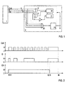
- Figure 1 are a first device, for example a Microcontroller 1, and a second device, for example a high-frequency IC implemented in bipolar circuit technology, for example a bipolar PLL, over a bus with three Lines 3, 4, 5 connected.
- the microcontroller 1 controls Data transmission to circuit 2 via the 3-wire bus as well as to further circuits and ensures the control of the Operating states of the circuit 2. This can either switched on operating state or a switched off Take up the operating state (stand-by).
- the 3-wire bus includes a first line 3 for transmitting a clock signal CLK, a second line 4 for transmitting a data signal D and a third line 5 for transmitting an enable signal EN. The latter signal serves to indicate the device 2, that the signals present on lines 3, 4 are valid for clock and data.
- the clock and data signals the lines 3, 4 can be in the facility during this time 2 can be received.
- the facility contains for data reception 2 a shift register 10 into which the data of the data signal D of line 4 can be read in serially.
- On Latch memory 11 takes over the data from shift register 10 in bit parallel form.
- the signals CLK and D are the Shift register 10 supplied, using the signal EN can be enabled via AND gates 12, 13. If the signal EN is deactivated, the data transfer is complete and the content of the shift register 10 is ins Latch 11 taken over.
- An OR switching element 20 is on the input side with the lines 3, 4, 5 connected. Through the output of the OR gate 20 an operating point setting device 21 controls the ensures that the receiving devices 10, ..., 13 and other functional units of the integrated circuit 2 with Reference voltages are supplied and thereby switched on.
- the circuits of the integrated circuit 2 are in bipolar circuit technology. For example, they contain bipolar differential amplifier switching stages whose Working points can be set using reference voltages. As is known, a bipolar differential amplifier comprises two emitter-coupled transistors using a current source Reference potential are connected. The reference voltage controls the power source. In addition, reference voltages are present, which one of the emitter-coupled transistors Activate differential amplifier. To switch on the integrated Circuit 2 are the reference voltages in the device 21 generated to switch off the integrated Circuit 2, these are switched off.
- the signal processing shown between times t0 and t4 takes place, for example, during an active Time slot within a mobile radio system, which after the TDMA process works. Only during such a time slot the controlled integrated circuit 2 is switched on. Power loss is only consumed during this time. Switching on and off is relatively quick, by evaluating the switching state of the OR gate 20.
- the assignment of the signal levels to the operating states (switched off: signals CLK, D, EN are L; switched on: at least one of the signals CLK, D, EN is H; Data transfer: Signal EN is H, signals CLK, D any; End of data transfer: Signal EN is L, at least one of the signals CLK, D is H) is chosen such that during the off Status of all functional units of device 2 are switched off and de-energized.
Description
Die Erfindung betrifft ein Verfahren zur Steuerung von Betriebszuständen einer zweiten Einrichtung von einer ersten Einrichtung aus, bei dem die Einrichtungen über Takt, Daten- und Freigabesignalleitungen miteinander verbunden sind, um die zweite Einrichtung ein- und auszuschalten. Die Erfindung betrifft außerdem eine entsprechende Schaltungsanordnung.The invention relates to a method for controlling operating states a second facility from a first Facility in which the facilities via clock, data and enable signal lines are connected to one another turn the second device on and off. The invention also relates to a corresponding circuit arrangement.
In elektronischen Geräten, in denen die Energieversorgungskapazität begrenzt ist, beispielsweise in akkubetriebenen Mobilfunkgeräten, werden integrierte Schaltungen, die zeitweise nicht benutzt sind, abgeschaltet, um Energie zu sparen. Dies wird insbesondere bei zeitschlitzgesteuertem Betrieb, beispielsweise nach dem TDMA-Verfahren (Time Division Multiple Access) angewandt, bei dem Sende- oder Empfangsbetrieb nur in aufeinanderfolgenden, beabstandeten Zeitschlitzen erfolgt. Hierzu steuert ein Microcontroller die Betriebszustände (d.h. eingeschaltet oder ausgeschaltet) weiterer im Gerät enthaltener integrierter Schaltungen.In electronic devices where the energy supply capacity is limited, for example in battery-operated mobile devices, become integrated circuits that temporarily are not used, switched off to save energy. This is used in particular in the case of time-slot-controlled operation, for example according to the TDMA (Time Division Multiple Access) applied, in the sending or receiving mode only in successive, spaced time slots. For this purpose, a microcontroller controls the operating states (i.e. switched on or switched off) further contained in the device integrated circuits.
In der EP-A-0 544 368 ist eine integrierte Schaltung beschrieben, bei der ein Power-Down-Zustand über verschiedene Signale einstellbar ist. Hierzu wird in einer Power-Down-Steuerschaltung eine Kombination verschiedener Zustände programmiert. Es erfolgt ein Vergleich eines zugeführten Eingangssignals mit der Programmierung, und davon abhängig wird eine weitere Schaltung gegebenenfalls deaktiviert. Die Power-Down-Steuerschaltung wertet eine spezifische Kombination von logischen Highs, logischen Lows und "don't care's" aus. An integrated circuit is described in EP-A-0 544 368, in which a power-down condition over various Signals is adjustable. This is done in a power down control circuit programmed a combination of different states. There is a comparison of an input signal supplied with programming, and depends on it another circuit may be deactivated. The power down control circuit evaluates a specific combination of logical highs, logical lows and "don't care's".
Die Aufgabe der Erfindung besteht darin, ein Verfahren und eine Schaltungsanordnung der eingangs genannten Art anzugeben, die möglichst geringen schaltungstechnischen Aufwand erfordern und eine schnelle Übertragung der Information zur Betriebszustandssteuerung ermöglichen.The object of the invention is a method and to specify a circuit arrangement of the type mentioned at the outset, require the least possible circuitry outlay and a fast transmission of the information for operating state control enable.
Erfindungsgemäß wird diese Aufgabe durch ein Verfahren gemäß
den Merkmalen des Patentanspruchs 1 gelöst. Eine Schaltungsanordnung
ist in Patentanspruch 3 angegeben.According to the invention, this object is achieved by a method according to
solved the features of
Zur Realisierung der Erfindung sind nur die ohnehin zur übrigen Datenübertragung erforderlichen Signalleitungen für Takt, Daten und Freigabe erforderlich. Zur Umschaltung in den eingeschalteten Zustand bzw. zur Rückschaltung in den ausgeschalteten Zustand ist jeweils nur die Überwachung der Signalpegel zu einem Zeitpunkt erforderlich, so daß die Übertragung der Steuerinformation nur eine geringe Zeitdauer beansprucht. Das Umschalten zwischen den Betriebszuständen erfolgt dementsprechend schnell.To implement the invention, only those to the rest are anyway Data transmission required signal lines for clock, Data and approval required. For switching to the switched on State or to switch back to the switched off The status is only the monitoring of the signal level required at a time so that the transfer the control information takes only a short period of time. Switching between the operating states takes place accordingly quickly.
Andere Lösungen sehen hier eine zusätzlich Leitung vor, die einerseits ein zusätzliches Eingangspin am Gehäuse der integrierten Schaltung erfordern würde und andererseits bei Hochfrequenzanwendungen in Mobilfunkgeräten zusätzlichen Tiefpaßfilteraufwand.Other solutions provide an additional line here, the on the one hand an additional input pin on the housing of the integrated Would require circuitry and on the other hand in high frequency applications additional low-pass filtering in mobile devices.
Zur schaltungstechnischen Realisierung in der integrierten Schaltung der gesteuerten Einrichtung ist im wesentlichen ein ODER-Schaltglied erforderlich, das mit dem 3-Leiter-Bus verbunden ist. Bei Realisierung in Bipolarschaltungstechnik wird vorteilhafterweise durch das ODER-Schaltglied ein die integrierte Schaltung versorgender Referenzspannungsgenerator gesteuert.For implementation in the integrated circuit Circuit of the controlled device is essentially a OR switching element required, which is connected to the 3-wire bus is. When implemented in bipolar circuit technology advantageously through the OR switching element an integrated Circuit supplying reference voltage generator controlled.
Nachfolgend wird die Erfindung anhand der in der Zeichnung dargestellten Figuren näher erläutert. Es zeigen:
Figur 1- ein Prinzipschaltbild zur Realisierung der Erfindung und
Figur 2- ein Signaldiagramm des 3-Leiter-Busses.
- Figure 1
- a schematic diagram for implementing the invention and
- Figure 2
- a signal diagram of the 3-wire bus.
Gemäß Figur 1 sind eine erste Einrichtung, zum Beispiel ein
Microcontroller 1, und eine zweite Einrichtung, zum Beispiel
ein in bipolarer Schaltungstechnik ausgeführter Hochfrequenz-IC,
beispielsweise eine bipolare PLL, über einen Bus mit drei
Leitungen 3, 4, 5 verbunden. Der Microcontroller 1 steuert
über den 3-Leiter-Bus die Datenübertragung zur Schaltung 2
sowie zu weiteren Schaltungen und sorgt für die Steuerung der
Betriebszustände der Schaltung 2. Diese kann entweder einen
eingeschalteten Betriebszustand oder einen ausgeschalteten
Betriebszustand (Stand-By) einnehmen. Der 3-Leiter-Bus umfaßt
eine erste Leitung 3 zur Übertragung eines Taktsignals CLK,
eine zweite Leitung 4 zur Übertragung eines Datensignals D
sowie eine dritte Leitung 5 zur Übertragung eines Freigabesignals
EN. Letzteres Signal dient dazu, der Einrichtung 2 anzuzeigen,
daß die an den Leitungen 3, 4 anliegenden Signale
für Takt und Daten gültig sind. Die Takt- und Datensignale
der Leitungen 3, 4 können während dieser Zeit in der Einrichtung
2 empfangen werden. Zum Datenempfang enthält die Einrichtung
2 ein Schieberegister 10, in das die Daten des Datensignals
D der Leitung 4 seriell eingelesen werden. Ein
Latch-Speicher 11 übernimmt die Daten des Schieberegisters 10
in bitparalleler Form. Die Signale CLK und D werden dem
Schieberegister 10 zugeführt, wobei sie mittels des Signals
EN über UND-Gatter 12, 13 freigeschaltet werden. Wenn das Signal
EN deaktiviert wird, ist die Datenübertragung abgeschlossen
und der Inhalt des Schieberegisters 10 wird ins
Latch 11 übernommen.According to Figure 1 are a first device, for example a
Ein ODER-Schaltglied 20 ist eingangsseitig mit den Leitungen
3, 4, 5 verbunden. Durch den Ausgang des ODER-Gatters 20 wird
eine Arbeitspunkteinstellungseinrichtung 21 gesteuert, die
dafür sorgt, daß die Empfangseinrichtungen 10, ..., 13 sowie
weitere Funktionseinheiten der integrierten Schaltung 2 mit
Referenzspannungen versorgt und dadurch eingeschaltet werden.
Die Schaltkreise der integrierten Schaltung 2 sind dabei in
bipolarer Schaltungstechnik ausgeführt. Sie enthalten beispielsweise
bipolare Differenzverstärkerschaltstufen, deren
Arbeitspunkte mittels Referenzspannungen einstellbar sind.
Bekanntlich umfaßt ein bipolarer Differenzverstärker zwei
emittergekoppelte Transistoren, die über eine Stromquelle mit
Bezugspotential verbunden sind. Die Referenzspannung steuert
die Stromquelle. Darüber hinaus können Referenzspannungen
vorliegen, die einen der emittergekoppelten Transistoren des
Differenzverstärkers ansteuern. Zum Einschalten der integrierten
Schaltung 2 werden in der Einrichtung 21 die Referenzspannungen
erzeugt, zum Ausschalten der integrierten
Schaltung 2 werden diese abgeschaltet.An
Anhand des in der Figur 2 dargestellten Signaldiagramms für
die Signale CLK, D, EN wird ein Beispiel für eine Datenübertragung
zwischen den Einrichtungen 1, 2 einschließlich Umschaltungen
zwischen den Betriebszuständen der Einrichtung 2
erläutert. Vor dem Zeitpunkt t0 führen alle drei Signalleitungen
einen L-Pegel. Ein L-Pegel liegt bei einem niedrigen
Potential, ein H-Pegel im Vergleich dazu bei höherem, positiverem
Potential. Das ODER-Gatter 20 ist gesperrt, so daß die
Einrichtung 21 keine Referenzspannungen zur Verfügung stellt
und dadurch die bipolare integrierte Schaltung 2 abgeschaltet
ist. Zum Zeitpunkt t0 schalten die drei Signale CLK, D, EN
auf einen H-Pegel. Das ODER-Gatter 20 wird aktiviert, so daß
von der Einrichtung 21 die Referenzspannungen bereitgestellt
werden und die integrierte Schaltung 2 eingeschaltet wird.
Die Zeitdauer bis zum Zeitpunkt t1 ist erforderlich, um die
Referenzspannungen in der Einrichtung 1 hochzufahren. Anschließend
erfolgt eine Datenübertragung, bei der das Taktsignal
CLK den Datentakt überträgt, das Datensignal D digitale
Daten in Form von L- und H-Impulsen überträgt und das Freigabesignal
EN einen H-Pegel aufweist. Zum Zeitpunkt t3 ist die
Datenübertragung abgeschlossen. Das Freigabesignal EN schaltet
auf einen L-Pegel. Durch Schaltungsmaßnahmen innerhalb
des Microcontrollers 1 wird gewährleistet, daß zum Zeitpunkt
t2 unmittelbar vorher mindestens eines der Signale CLK oder D
(im dargestellten Beispiel beide Signale) einen H-Pegel aufweist.
Das ODER-Gatter 20 ist dann auch nach Abschluß der Datenübertragung
aktiv und die integrierte Schaltung 2 bleibt
eingeschaltet. Zwischen den Zeitpunkten t3 und t4 erfolgt die
Verarbeitung der übertragenen Daten. Zum Zeitpunkt t4 werden
auch die Signale CLK und D auf einen L-Pegel geschaltet, so
daß das ODER-Gatter sperrt und die integrierte Schaltung 2
wieder in den abgeschalteten Betriebszustand (Stand-By) übergeht. Using the signal diagram for
the signals CLK, D, EN becomes an example of a data transmission
between
Die zwischen den Zeitpunkten t0 und t4 dargestellte Signalverarbeitung
erfolgt beispielsweise während eines aktiven
Zeitschlitzes innerhalb eines Mobilfunksystems, das nach dem
TDMA-Verfahren arbeitet. Nur während eines solchen Zeitschlitzes
ist die gesteuerte integrierte Schaltung 2 eingeschaltet.
Nur während dieser Zeit wird Verlustleistung verbraucht.
Das Ein- und Ausschalten erfolgt relativ schnell,
indem der Schaltzustand des ODER-Gatters 20 ausgewertet wird.
Die Zuordnung der Signalpegel zu den Betriebszuständen
(ausgeschaltet: Signale CLK, D, EN sind L; eingeschaltet:
mindestens eines der Signale CLK, D, EN ist H; Datenübertragung:
Signal EN ist H, Signale CLK, D beliebig; Ende der Datenübertragung:
Signal EN ist L, mindestens eines der Signale
CLK, D ist H) ist derart gewählt, daß während des ausgeschalteten
Zustands sämtliche Funktionseinheiten der Einrichtung 2
abgeschaltet und stromlos sind. Um im ausgeschalteten Zustand
die Einschaltbedingung zu erkennen, ist nicht erforderlich,
daß die Schaltkreise der integrierten Schaltung 2 vorher einen
bestimmten Schaltzustand eingenommen haben. Dies ist insbesondere
bei bipolaren Schaltungen vorteilhaft, da deren
Schaltglieder, zum Beispiel Differenzverstärkerschaltstufen,
unabhängig vom Schaltzustand (H oder L) bei eingeschaltetem
Betriebszustand stets einen Strom führen.The signal processing shown between times t0 and t4
takes place, for example, during an active
Time slot within a mobile radio system, which after the
TDMA process works. Only during such a time slot
the controlled integrated
Claims (5)
- Method for controlling operating states of a second device (2) by means of a first device (1),in which the devices (1, 2) are connected to one another by way of at least three signal lines (3, 4, 5), the first line (3) of which is designed to carry a clock signal (CLK), the second line (4) of which is designed to carry a data signal (D) representing digital data, and the third line (5) of which is designed to carry an enable signal (EN), which indicates that the transmission of the data signal and clock signal (D, CLK) is valid, characterized in thata first operating state, in which the second device (2) is switched off, is set when the signals on the lines (3, 4, 5) are brought to a first level (L) by the first device (1),a second operating state, in which the second device (2) is switched on, is set when the signals on the first, second and third lines (3, 4, 5) are brought to a second level (H) by the first device (1),the second level (H) having a more positive potential in comparison with the first level (L), in thatdata are transmitted during the second operating state by the second level (H) being transmitted on the third line (5) and the transmission of the data signal and clock signal (D, CLK) thereby being indicated as being valid and by the clock signal (CLK) which has alternating first and second levels (L, H), being transmitted on the first line (3) and by the data signal (D) representing the data being transmitted on the second line (4),and the enable signal (EN) has the first level (L) and at least one of the data and clock signals (D, CKL) has the second level (H) during the second operating state outside the period of time for transmitting data.
- Method according to Claim 1,
characterized in that
a control signal for switching-on purposes is generated in the second device (2) by ORing (20) the signals (CLK, D, EN) on the three lines (3, 4, 5). - Circuit arrangement for controlling operating states of a second device by means of a first device, having a first device (1) and a second device (2) and having at least three signal lines (3, 4, 5), the first line (3) of which is intended for transmitting a clock signal (CLK), the second line (4) of which is intended for transmitting a data signal (D) representing digital data, and the third line (5) of which is intended for transmitting an enable signal (EN), which indicates that the transmission of the data signal and clock signal (D, CLK) is valid, and having means (20, 21),which can be used to set a first operating state, in which the second device (2) is switched off, when the signals on the lines (3, 4, 5) are at a first level (L),which can be used to set a second operating state, in which the second device (2) is switched on, when the signals on the first, second and third lines (3, 4, 5) have a second level (H),the second level (H) having a more positive potential in comparison with the first level (L),which can be used to transmit data during the second operating state by it being possible to transmit the second level (H) on the third line (5) and by indicating that the data signal and clock signal (D, CLK) are valid, by it being possible to transmit the clock signal (CLK), which alternately has first and second levels (L, H), on the first line (3) and by it being possible to transmit the data signal (D) representing the data on the second line (4),and which can be used, during the second operating state outside the time in which data are transmitted, to generate the enable signal (EN) having a first level (L) and at least one of the data and clock signals having the second level (H).
- Circuit arrangement according to Claim 3,
characterized in that
the means (20, 21) comprise an OR switching element (20), which is connected to the lines (3, 4, 5) on the input side and can be used to generate a control signal on the output side, it being possible for said control signal to be used to switch a means (10, ..., 13) for receiving the data and further functional units of the second device (2) on and off. - Circuit arrangement according to either of Claims 3 and 4,
characterized in that
the second device (2) is designed using bipolar circuitry and has differential amplifier switching stages, the operating points of which can be set by means of reference voltages, and in that provision is made of means (21), which can be used to switch on the reference voltages during the second operating state and switch them off during the first operating state.
Applications Claiming Priority (2)
| Application Number | Priority Date | Filing Date | Title |
|---|---|---|---|
| DE19701911 | 1997-01-21 | ||
| DE19701911A DE19701911C2 (en) | 1997-01-21 | 1997-01-21 | Method and circuit arrangement for controlling operating states of a second device by a first device |
Publications (3)
| Publication Number | Publication Date |
|---|---|
| EP0862107A2 EP0862107A2 (en) | 1998-09-02 |
| EP0862107A3 EP0862107A3 (en) | 2002-06-05 |
| EP0862107B1 true EP0862107B1 (en) | 2004-04-07 |
Family
ID=7817890
Family Applications (1)
| Application Number | Title | Priority Date | Filing Date |
|---|---|---|---|
| EP98100560A Expired - Lifetime EP0862107B1 (en) | 1997-01-21 | 1998-01-14 | Method and circuit for controlling the operating state of a second device by means of a first device |
Country Status (3)
| Country | Link |
|---|---|
| US (1) | US5994931A (en) |
| EP (1) | EP0862107B1 (en) |
| DE (2) | DE19701911C2 (en) |
Families Citing this family (5)
| Publication number | Priority date | Publication date | Assignee | Title |
|---|---|---|---|---|
| US7069359B1 (en) * | 2000-04-03 | 2006-06-27 | Intel Corporation | Circuit and technique to stall the communication of data over a double pumped bus |
| US6796733B2 (en) | 2000-10-31 | 2004-09-28 | International Imaging Materials Inc. | Thermal transfer ribbon with frosting ink layer |
| EP1213638A1 (en) * | 2000-12-06 | 2002-06-12 | Siemens Aktiengesellschaft | Enabling devices |
| DE10103323A1 (en) * | 2001-01-25 | 2002-08-01 | Philips Corp Intellectual Pty | Bus system with low power phase |
| DE102005004105B4 (en) * | 2005-01-28 | 2013-05-08 | Intel Mobile Communications GmbH | Signal processing device and method for operating a signal processing device |
Family Cites Families (6)
| Publication number | Priority date | Publication date | Assignee | Title |
|---|---|---|---|---|
| DE2360635C3 (en) * | 1973-12-05 | 1979-02-22 | Siemens Ag, 1000 Berlin Und 8000 Muenchen | Arrangement for the connection of terminals to teletype or data networks |
| US4501975A (en) * | 1982-02-16 | 1985-02-26 | Sperry Corporation | Josephson junction latch circuit |
| US4906870A (en) * | 1988-10-31 | 1990-03-06 | Atmel Corporation | Low power logic array device |
| US5278581A (en) * | 1990-09-17 | 1994-01-11 | Kabushiki Kaisha Toshiba | Printer for printing and image formed of 2-dimensionally arranged pixels, and method of printing the same |
| US5227790A (en) * | 1991-01-31 | 1993-07-13 | Oki Electric Industry Co., Ltd. | Cascaded drive units having low power consumption |
| US5329178A (en) * | 1991-11-27 | 1994-07-12 | North American Philips Corporation | Integrated circuit device with user-programmable conditional power-down means |
-
1997
- 1997-01-21 DE DE19701911A patent/DE19701911C2/en not_active Expired - Lifetime
-
1998
- 1998-01-14 DE DE59811126T patent/DE59811126D1/en not_active Expired - Lifetime
- 1998-01-14 EP EP98100560A patent/EP0862107B1/en not_active Expired - Lifetime
- 1998-01-21 US US09/010,172 patent/US5994931A/en not_active Expired - Lifetime
Also Published As
| Publication number | Publication date |
|---|---|
| DE19701911C2 (en) | 1999-04-22 |
| EP0862107A2 (en) | 1998-09-02 |
| DE19701911A1 (en) | 1998-07-23 |
| EP0862107A3 (en) | 2002-06-05 |
| DE59811126D1 (en) | 2004-05-13 |
| US5994931A (en) | 1999-11-30 |
Similar Documents
| Publication | Publication Date | Title |
|---|---|---|
| EP0502518B1 (en) | Wireless data transmission method on a data carrier | |
| DE60203637T2 (en) | CONTACT-FREE INTEGRATED CIRCUIT WITH AUTOMATIC FRAME IDENTIFICATION AGENTS | |
| DE2654050C3 (en) | Clock signal control system of a microcomputer system | |
| EP0583690B1 (en) | Chip card with field intensity detector | |
| EP0590122B1 (en) | Process and system for transmitting serial data structures for information carrier identification systems, and information carriers | |
| EP0264470B1 (en) | Method for digital control of the output signal edge steepness of lsi semiconductor chip power amplifiers designated for use in a computer | |
| DE4131222A1 (en) | CONTACT-FREE WORKING IS CARD AND METHOD FOR USING THE SAME | |
| EP0895394A2 (en) | Radiotelephone | |
| DE19614237C1 (en) | Communication system with a master station and at least one slave station | |
| DE10317289A1 (en) | Integrated circuit with multiple communication modes and associated operating procedure | |
| EP1573664B1 (en) | Device for determining the energy level of an energy store of a mobile data carrier | |
| EP0509125B1 (en) | Device for contactless data and energy transmission and operating method | |
| EP0949576B1 (en) | Data carrier and method for wireless reception of data and energy | |
| DE19614238C1 (en) | Communication system with a master station and at least one slave station | |
| EP0862107B1 (en) | Method and circuit for controlling the operating state of a second device by means of a first device | |
| DE19937829A1 (en) | Data input-output circuit for integrated circuit devices e.g. memory devices has a number of output units and a control unit | |
| EP0863639B1 (en) | Data transmission system | |
| DE3628526A1 (en) | ENERGY SAVING SECURITY SYSTEM | |
| EP1110300B1 (en) | Power supply device and circuit associated with said power supply device | |
| EP1046125B1 (en) | Data carrier | |
| EP2141637B1 (en) | Portable data carrier with active contactless interface and operating method | |
| DE102008040453B4 (en) | Non-contact communication device and method for contactless communication | |
| AT401127B (en) | CONTACTLESS DATA TRANSFER SYSTEM | |
| EP0496024B1 (en) | Method to reduce power loss in contactless data and power transmission devices and means to carry out this method | |
| EP0840229A2 (en) | Apparatus and method for selecting address words |
Legal Events
| Date | Code | Title | Description |
|---|---|---|---|
| PUAI | Public reference made under article 153(3) epc to a published international application that has entered the european phase |
Free format text: ORIGINAL CODE: 0009012 |
|
| AK | Designated contracting states |
Kind code of ref document: A2 Designated state(s): AT BE CH DE DK ES FI FR GB GR IE IT LI LU MC NL PT SE |
|
| AX | Request for extension of the european patent |
Free format text: AL;LT;LV;MK;RO;SI |
|
| RAP1 | Party data changed (applicant data changed or rights of an application transferred) |
Owner name: INFINEON TECHNOLOGIES AG |
|
| PUAL | Search report despatched |
Free format text: ORIGINAL CODE: 0009013 |
|
| AK | Designated contracting states |
Kind code of ref document: A3 Designated state(s): AT BE CH DE DK ES FI FR GB GR IE IT LI LU MC NL PT SE |
|
| AX | Request for extension of the european patent |
Free format text: AL;LT;LV;MK;RO;SI |
|
| RIC1 | Information provided on ipc code assigned before grant |
Free format text: 7G 06F 1/26 A, 7H 04B 1/16 B, 7H 03K 19/00 B |
|
| 17P | Request for examination filed |
Effective date: 20021202 |
|
| AKX | Designation fees paid |
Designated state(s): DE FR GB IT |
|
| 17Q | First examination report despatched |
Effective date: 20030217 |
|
| GRAP | Despatch of communication of intention to grant a patent |
Free format text: ORIGINAL CODE: EPIDOSNIGR1 |
|
| GRAS | Grant fee paid |
Free format text: ORIGINAL CODE: EPIDOSNIGR3 |
|
| GRAA | (expected) grant |
Free format text: ORIGINAL CODE: 0009210 |
|
| AK | Designated contracting states |
Kind code of ref document: B1 Designated state(s): DE FR GB IT |
|
| REG | Reference to a national code |
Ref country code: GB Ref legal event code: FG4D Free format text: NOT ENGLISH |
|
| REF | Corresponds to: |
Ref document number: 59811126 Country of ref document: DE Date of ref document: 20040513 Kind code of ref document: P |
|
| REG | Reference to a national code |
Ref country code: IE Ref legal event code: FG4D Free format text: GERMAN |
|
| GBT | Gb: translation of ep patent filed (gb section 77(6)(a)/1977) |
Effective date: 20040602 |
|
| ET | Fr: translation filed | ||
| REG | Reference to a national code |
Ref country code: IE Ref legal event code: FD4D |
|
| PLBE | No opposition filed within time limit |
Free format text: ORIGINAL CODE: 0009261 |
|
| STAA | Information on the status of an ep patent application or granted ep patent |
Free format text: STATUS: NO OPPOSITION FILED WITHIN TIME LIMIT |
|
| 26N | No opposition filed |
Effective date: 20050110 |
|
| REG | Reference to a national code |
Ref country code: FR Ref legal event code: TP Owner name: INTEL MOBILE COMMUNICATIONS GMBH, DE Effective date: 20120404 Ref country code: FR Ref legal event code: CA Effective date: 20120404 |
|
| REG | Reference to a national code |
Ref country code: GB Ref legal event code: 732E Free format text: REGISTERED BETWEEN 20120607 AND 20120613 |
|
| REG | Reference to a national code |
Ref country code: GB Ref legal event code: 732E Free format text: REGISTERED BETWEEN 20121213 AND 20121219 |
|
| REG | Reference to a national code |
Ref country code: DE Ref legal event code: R081 Ref document number: 59811126 Country of ref document: DE Owner name: INTEL DEUTSCHLAND GMBH, DE Free format text: FORMER OWNER: INTEL MOBILE COMMUNICATIONS GMBH, 85579 NEUBIBERG, DE Effective date: 20130315 Ref country code: DE Ref legal event code: R081 Ref document number: 59811126 Country of ref document: DE Owner name: INTEL DEUTSCHLAND GMBH, DE Free format text: FORMER OWNER: INFINEON TECHNOLOGIES AG, 85579 NEUBIBERG, DE Effective date: 20130315 Ref country code: DE Ref legal event code: R081 Ref document number: 59811126 Country of ref document: DE Owner name: INTEL DEUTSCHLAND GMBH, DE Free format text: FORMER OWNER: INFINEON TECHNOLOGIES AG, 81669 MUENCHEN, DE Effective date: 20130314 Ref country code: DE Ref legal event code: R081 Ref document number: 59811126 Country of ref document: DE Owner name: INTEL DEUTSCHLAND GMBH, DE Free format text: FORMER OWNER: INTEL MOBILE COMMUNICATIONS TECHNOLOGY GMBH, 85579 NEUBIBERG, DE Effective date: 20130326 Ref country code: DE Ref legal event code: R081 Ref document number: 59811126 Country of ref document: DE Owner name: INTEL MOBILE COMMUNICATIONS GMBH, DE Free format text: FORMER OWNER: INFINEON TECHNOLOGIES AG, 85579 NEUBIBERG, DE Effective date: 20130315 Ref country code: DE Ref legal event code: R081 Ref document number: 59811126 Country of ref document: DE Owner name: INTEL MOBILE COMMUNICATIONS GMBH, DE Free format text: FORMER OWNER: INFINEON TECHNOLOGIES AG, 81669 MUENCHEN, DE Effective date: 20130314 Ref country code: DE Ref legal event code: R081 Ref document number: 59811126 Country of ref document: DE Owner name: INTEL MOBILE COMMUNICATIONS GMBH, DE Free format text: FORMER OWNER: INTEL MOBILE COMMUNICATIONS TECHNOLOGY GMBH, 85579 NEUBIBERG, DE Effective date: 20130326 Ref country code: DE Ref legal event code: R081 Ref document number: 59811126 Country of ref document: DE Owner name: INTEL MOBILE COMMUNICATIONS GMBH, DE Free format text: FORMER OWNER: INTEL MOBILE COMMUNICATIONS GMBH, 85579 NEUBIBERG, DE Effective date: 20130315 |
|
| REG | Reference to a national code |
Ref country code: FR Ref legal event code: PLFP Year of fee payment: 18 |
|
| PGFP | Annual fee paid to national office [announced via postgrant information from national office to epo] |
Ref country code: IT Payment date: 20150119 Year of fee payment: 18 |
|
| PGFP | Annual fee paid to national office [announced via postgrant information from national office to epo] |
Ref country code: GB Payment date: 20150114 Year of fee payment: 18 Ref country code: FR Payment date: 20150108 Year of fee payment: 18 |
|
| REG | Reference to a national code |
Ref country code: DE Ref legal event code: R081 Ref document number: 59811126 Country of ref document: DE Owner name: INTEL DEUTSCHLAND GMBH, DE Free format text: FORMER OWNER: INTEL MOBILE COMMUNICATIONS GMBH, 85579 NEUBIBERG, DE |
|
| REG | Reference to a national code |
Ref country code: FR Ref legal event code: CD Owner name: INTEL DEUTSCHLAND GMBH, DE Effective date: 20160126 |
|
| PGFP | Annual fee paid to national office [announced via postgrant information from national office to epo] |
Ref country code: DE Payment date: 20160105 Year of fee payment: 19 |
|
| GBPC | Gb: european patent ceased through non-payment of renewal fee |
Effective date: 20160114 |
|
| REG | Reference to a national code |
Ref country code: FR Ref legal event code: ST Effective date: 20160930 |
|
| PG25 | Lapsed in a contracting state [announced via postgrant information from national office to epo] |
Ref country code: GB Free format text: LAPSE BECAUSE OF NON-PAYMENT OF DUE FEES Effective date: 20160114 |
|
| PG25 | Lapsed in a contracting state [announced via postgrant information from national office to epo] |
Ref country code: FR Free format text: LAPSE BECAUSE OF NON-PAYMENT OF DUE FEES Effective date: 20160201 |
|
| PG25 | Lapsed in a contracting state [announced via postgrant information from national office to epo] |
Ref country code: IT Free format text: LAPSE BECAUSE OF NON-PAYMENT OF DUE FEES Effective date: 20160114 |
|
| REG | Reference to a national code |
Ref country code: DE Ref legal event code: R119 Ref document number: 59811126 Country of ref document: DE |
|
| PG25 | Lapsed in a contracting state [announced via postgrant information from national office to epo] |
Ref country code: DE Free format text: LAPSE BECAUSE OF NON-PAYMENT OF DUE FEES Effective date: 20170801 |