EP1573664B1 - Device for determining the energy level of an energy store of a mobile data carrier - Google Patents
Device for determining the energy level of an energy store of a mobile data carrier Download PDFInfo
- Publication number
- EP1573664B1 EP1573664B1 EP03799415A EP03799415A EP1573664B1 EP 1573664 B1 EP1573664 B1 EP 1573664B1 EP 03799415 A EP03799415 A EP 03799415A EP 03799415 A EP03799415 A EP 03799415A EP 1573664 B1 EP1573664 B1 EP 1573664B1
- Authority
- EP
- European Patent Office
- Prior art keywords
- auxiliary capacitor
- data carrier
- measurement circuit
- energy
- voltage
- Prior art date
- Legal status (The legal status is an assumption and is not a legal conclusion. Google has not performed a legal analysis and makes no representation as to the accuracy of the status listed.)
- Expired - Lifetime
Links
Images


Classifications
-
- G—PHYSICS
- G06—COMPUTING; CALCULATING OR COUNTING
- G06K—GRAPHICAL DATA READING; PRESENTATION OF DATA; RECORD CARRIERS; HANDLING RECORD CARRIERS
- G06K19/00—Record carriers for use with machines and with at least a part designed to carry digital markings
- G06K19/06—Record carriers for use with machines and with at least a part designed to carry digital markings characterised by the kind of the digital marking, e.g. shape, nature, code
- G06K19/067—Record carriers with conductive marks, printed circuits or semiconductor circuit elements, e.g. credit or identity cards also with resonating or responding marks without active components
- G06K19/07—Record carriers with conductive marks, printed circuits or semiconductor circuit elements, e.g. credit or identity cards also with resonating or responding marks without active components with integrated circuit chips
- G06K19/0701—Record carriers with conductive marks, printed circuits or semiconductor circuit elements, e.g. credit or identity cards also with resonating or responding marks without active components with integrated circuit chips at least one of the integrated circuit chips comprising an arrangement for power management
-
- G—PHYSICS
- G06—COMPUTING; CALCULATING OR COUNTING
- G06K—GRAPHICAL DATA READING; PRESENTATION OF DATA; RECORD CARRIERS; HANDLING RECORD CARRIERS
- G06K19/00—Record carriers for use with machines and with at least a part designed to carry digital markings
- G06K19/06—Record carriers for use with machines and with at least a part designed to carry digital markings characterised by the kind of the digital marking, e.g. shape, nature, code
- G06K19/067—Record carriers with conductive marks, printed circuits or semiconductor circuit elements, e.g. credit or identity cards also with resonating or responding marks without active components
- G06K19/07—Record carriers with conductive marks, printed circuits or semiconductor circuit elements, e.g. credit or identity cards also with resonating or responding marks without active components with integrated circuit chips
- G06K19/0723—Record carriers with conductive marks, printed circuits or semiconductor circuit elements, e.g. credit or identity cards also with resonating or responding marks without active components with integrated circuit chips the record carrier comprising an arrangement for non-contact communication, e.g. wireless communication circuits on transponder cards, non-contact smart cards or RFIDs
Definitions
- the invention relates to a device for determining the energy state of an energy storage of a mobile data carrier.
- a device for determining the energy state of an energy storage of a mobile data carrier can be used, for example, in connection with contactless identification systems.
- Non-contact identification systems work on the basis of non-contact transmission technologies. These can be based on an electromagnetic transmission or a transmission by means of light, infrared or ultrasonic signals. Systems of this type are used for example for the identification of persons or moving goods such as means of transport.
- the necessary data is to be transmitted from a transceiver via a non-contact data link, for example via an air interface to a disk and back.
- the non-contact identification technology also allows detection of data during a passing movement of the data carrier on the transceiver, without the data carrier has to be inserted into a read / write device or pulled through this.
- Data carriers of this kind are used, for example, as tickets with an electronically rechargeable credit, the respective amount being debited automatically when using the means of transport.
- the IC card has, inter alia, a data transmission / reception device, a data processing device, a charging device, a comparison device and a time measuring device.
- a method for controlling the charging and discharging phases of a backup capacitor is known.
- a constant current source is formed by a current mirror circuit and compared via a comparator, the voltage on the backup capacitor with a bandgap reference.
- the data carriers In order that the data carriers can be used indefinitely, they do not require the integration of chemical energy stores, such as batteries.
- the necessary electrical energy of the disk is therefore externally, d. H. taken from an originating from the transceiver energy source, such as an electric or magnetic field, contactless.
- the transceiver energy source such as an electric or magnetic field, contactless.
- suitable transmission and coding methods are necessary.
- only certain frequency bands are usually released for the transmission of data, for example the ISM frequency bands (Industrial, Scientific & Medical) for industrial, scientific and medical applications.
- Possible national radio regulations can specify, among other things, the modulation bandwidths to be maintained and the field strengths.
- the transmission and coding methods must also ensure an energetic supply of the electronics on the data carrier.
- the time ratio of switched on to off carrier frequency prevail.
- consecutive changes from on to off carrier frequency continue to contribute to a significant increase in sideband modulation.
- the need to comply with the sideband limits specified in the standard results in a maximum possible data rate.
- data transmission in non-contact transmission techniques may be undesirably affected by insufficient coupling.
- insufficient coupling can be present, for example, when a mobile data carrier moves very quickly through a field, or even at the field boundaries, where the energy transfer is low.
- the object of the invention is to show a way how the disadvantages described above can be avoided.
- the advantages of the invention are, in particular, that information about the energy state of the mobile data carrier can be made available to the user at any desired time. Thus, it is possible to detect an insufficient energy state of the energy storage device of the mobile data carrier and to correctly and completely perform a data exchange that is incomplete or faulty due to the insufficient energy state. This option can be implemented on the mobile data carrier with only a small additional effort.
- a device according to the invention provides fast and good information about the energy state of the energy storage of the mobile data carrier.
- Another advantage of the invention is an almost complete independence of the obtained statements of tolerances involved circuit elements.
- FIG. 1 shows a block diagram in which the components of an identification system essential for understanding the invention are shown.
- the system shown has a read / write device 1 and a mobile data carrier 4. Furthermore, a bidirectional exchange of data D takes place via an air transmission path 3 between the read / write device 1 and the mobile data carrier 4. Furthermore, the read / write device also transmits energy E to the mobile data carrier 4 via the air transmission path 3, this transmission of energy into Time intervals are made in which no exchange of data takes place.
- the transmission of data and energy is based on the principle of inductive coupling.
- the read / write device 1 is provided with a coil 2 and the mobile data carrier 4 with a coil 5.
- the transmitted energy via a rectifier 6 is fed to a realized as a capacitor energy storage.
- the voltage applied to the capacitor 7 unstabilized DC voltage is fed to a voltage stabilizer 9, at the output of which the supply of the mobile data carrier 4 required stabilized DC voltage is provided.
- the capacitor 7 is connected to a device 8, which is provided for determining the energy state of the capacitor 7.
- the device 8 has a current mirror 11 comprising transistors 11 and 12. This has two parallel paths. In the first path, in which the transistor 12 is located, a current I 0 flows . In the second path, in which the transistor 11 is arranged, a current I R flows . In the second path there is further provided an ohmic resistor 14 connected to the transistor 11, the other terminal of which is connected to a HIGH / LOW level signal input 20 of the device 8. About this input 20 of the device 8 is supplied by a logic, not shown, either a high-level signal or a low-level signal.
- an auxiliary capacitor 13 is connected to the transistor 12, whose other terminal is grounded.
- the ground remote terminal of the auxiliary capacitor 13 is connected to an input of an EX-OR gate 16 and to the collector of an NPN transistor 15.
- the emitter of the transistor 15 is grounded.
- the base of the transistor 15 is connected via an ohmic resistor 21 to an input 17 of the device 8.
- the input 17 is a measuring time input, via which the device 8 signals are supplied, which define measuring time intervals. These measurement time signals are generated in the aforementioned logic, not shown, which also provides the signals provided at the HIGH-LOW level signal input 20 available. In this logic is information about the system clock, which are needed to generate the inputs 17 and 20 supplied signals.
- the measuring input signals applied to the input 17 are supplied to the other input of the EX-OR gate 16 and the ohmic resistor 21 of the base of the npn transistor 15.
- the output signals of the EX-OR element 16, which is information about charging times of the auxiliary capacitor 13, are fed to an evaluation logic 18. From the said charging times, this calculates a quantity in the form of a numerical value, which gives information about the energy state of the capacitor 7.
- this numerical value contains information about the ratio of the unstabilized supply voltage applied to the capacitor 7 to the stabilized DC voltage required by the mobile data carrier as the supply voltage.
- the latter is for example 3 V and is the operating voltage of a chip of the mobile data carrier.
- information can be made in particular a statement about how large the energy reserve of the mobile data carrier at the time of measurement.
- I 0 I R 1 - 2 ⁇ + 2 ⁇ 1.
- I R ( U L ) U 3 - U L R 14 ,
- Equation 3 The useful scope of Equation 3 is the range of UH ⁇ U3 and U3-UH> 0.
- FIG. 3 shows a diagram for illustrating different voltages of FIG. 2.
- the distance S of the read / write device 1 from the mobile data carrier 4 and along the ordinate the inductive coupling or the coupling factor k are plotted. It can be seen that the LOW level signal UL and the HIGH level signal UH are each constant regardless of the distance S and that the voltage U1, which is applied to the capacitor 7, becomes smaller with increasing distance S.
- FIG. 4 shows a diagram for illustrating the voltage profile of the unstabilized voltage U1 applied to the capacitor 7 of FIG. 2 as a function of the distance between the read / write device 1 and the mobile data carrier 4. This bell-shaped voltage characteristic also exists when the mobile data carrier 4 at the same distance parallel to the read / write device 1 is passed.
- FIG. 5 shows a diagram for illustrating the position of two measuring times or measuring time intervals. If the mobile data carrier 4 is moved parallel to the read / write device 1 at a constant distance S, then the voltage U1 on the capacitor 7 has the illustrated time profile, which is bell-shaped. According to the invention, two arbitrary measurement times or measurement time intervals are defined, wherein the voltage value at the measurement time t1 is comparatively small and relatively large at the measurement time t2. As is apparent from FIGS. 6 and 7, different charging times result at the measuring times from which conclusions can be drawn about the energy state of the capacitor 7 of the mobile data carrier 4 and thus also can be drawn on the working capacity of the mobile data carrier 4.
- FIG. 6 shows a diagram for illustrating the measured charging times during a measurement at the first measuring time t1, at which a comparatively small voltage U1 is applied to the capacitor 7.
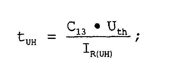
- 6 shows the signal UH or UL present at the input 20, an integration time signal in the track b, the measurement time signal applied to the input 17 in the track c, the threshold voltage U th in the track d and in the track e is applied to the auxiliary capacitor 13 voltage U4.
- the signal UH or UL shown in the track a and the measuring time signal shown in the track c are not shown Logic specified in which information about the system clock is available.
- the measurement time signal is started when the signal shown in track a transitions from the HIGH to the LOW state.
- the integration time interval shown in the lane b also starts.
- the charging of the auxiliary capacitor 13 by the charging current I 0 (UL) begins at this time.
- the charging process is continued until the voltage across the auxiliary capacitor 13 reaches the threshold voltage U th shown in the track d.
- the integration time is terminated and provided as the charging time t UL of the evaluation logic 18.
- the measuring time interval is ended, as can be seen from the track c.
- the auxiliary capacitor 13 is discharged by the then conducting transistor 15.
- the HIGH-LOW level signal shown in the track a has the HIGH level and the auxiliary capacitor 13 is discharged, then - as is apparent from the second falling edge of the measuring time signal shown in the track c - a second measuring time interval is started.
- a measurement of the integration time begins again, as can be seen from the second rising edge of the integration time signal shown in the track b.
- charging of the auxiliary capacitor 13 by the charging current I 0 (UH) also begins at this time.
- the charging process is continued until the voltage across the auxiliary capacitor 13 reaches the threshold voltage U th shown in the track d.
- the integration time is ended and provided as the charging time t UH of the evaluation logic 18. If, after this time, the measuring time signal returns to the HIGH state, this measuring time interval is also ended and the auxiliary capacitor 13 is discharged via the then conducting transistor 15.
- FIG. 7 shows a diagram for illustrating the measured charging times during a measurement at the second measuring time t 2, at which a comparatively large voltage U 1 is applied to the capacitor 7.
- 7 shows the signal UH or UL present at the input 20, an integration time signal in the track b, the measurement time signal applied to the input 17 in the track c, the threshold voltage U th in the track d and in the track e is applied to the auxiliary capacitor 13 voltage U4.
- the signal UH or UL shown in the track a and the measuring time signal shown in the track c are given by the unsigned logic in which information about the system clock are present.
- the measurement time signal is started when the signal shown in track a transitions from the HIGH to the LOW state.
- the integration time interval shown in the lane b also starts.
- the charging of the auxiliary capacitor 13 by the charging current I 0 (UL) begins at this time.
- the charging process is continued until the voltage across the auxiliary capacitor 13 reaches the threshold voltage U th shown in the track d.
- the integration time is terminated and provided as the charging time t UL of the evaluation logic 18.
- the measuring time interval is ended, as can be seen from the track c.
- the auxiliary capacitor 13 is discharged by the then conducting transistor 15.
- the HIGH-LOW level signal shown in the track a has the HIGH level and the auxiliary capacitor 13 is discharged, then - as is apparent from the second falling edge of the measuring time signal shown in the track c - a second measuring time interval is started.
- a measurement of the integration time begins again, as can be seen from the second rising edge of the integration time signal shown in the track b. It also starts to this Time also a charging of the auxiliary capacitor 13 by the charging current I 0 (UH) .
- the charging process is continued until the voltage across the auxiliary capacitor 13 reaches the threshold voltage U th shown in the track d.
- the integration time is ended and provided as the charging time t UH of the evaluation logic 18. If, after this time, the measuring time signal returns to the HIGH state, this measuring time interval is also ended and the auxiliary capacitor 13 is discharged via the then conducting transistor 15.
- the evaluation logic 18 in each case forms the quotient of the charging times t UL and t UH and makes these quotients available as the quantity describing the energy state of the capacitor 7 at the output 19 of the device 8. From there it is fed to a transmitting unit of the mobile data carrier 4 and transmitted via the air transmission path 3 to the read / write device 1. There it is available for a display, by means of which a user can assess the energy state of the capacitor 7 of the mobile data carrier 4 and if necessary initiate appropriate measures. Alternatively, the transmitted to the read / write device 1, the energy state of the capacitor 7 descriptive size can also be evaluated by an automatic unit in the read / write device 1, which automatically directs appropriate measures if necessary.
Abstract
Description
Vorrichtung zur Ermittlung des Ermittlung des Ernergiezustandes eines Energiespeichers eines mobilen DatenträgersDevice for determining the determination of the energy state of an energy storage of a mobile data carrier
Die Erfindung betrifft eine Vorrichtung zur Ermittlung des Energiezustandes eines Energiespeichers eines mobilen Datenträgers. Eine derartige Vorrichtung kann beispielsweise im Zusammenhang mit kontaktlosen Identifikationssystemen verwendet werden.The invention relates to a device for determining the energy state of an energy storage of a mobile data carrier. Such a device can be used, for example, in connection with contactless identification systems.
Kontaktlose Identifikationssysteme arbeiten auf Basis von berührungslosen Übertragungstechniken. Diese können beruhen auf einer elektromagnetischen Übertragung oder einer Übertragung mittels Licht-, Infrarot- oder Ultraschallsignalen. Systeme dieser Art werden beispielsweise zur Identifikation von Personen oder von bewegten Gütern wie beispielsweise Transportmittel eingesetzt. Die notwendigen Daten werden dazu von einem Sende-/Empfangsgerät über eine berührungslose Datenübertragungsstrecke übertragen, beispielsweise über eine Luftschnittstelle zu einem Datenträger und zurück. Dabei gestattet die berührungslose Identtechnik auch eine Erfassung von Daten während einer Vorbeibewegung des Datenträgers am Sende-/Empfangsgerät, ohne dass der Datenträger in ein Schreib-/Lesegerät eingeschoben oder durch dieses gezogen werden muss. Datenträger dieser Art werden beispielsweise als Fahrkarten mit einem elektronisch nachladbaren Guthaben verwendet, wobei der jeweilige Betrag bei einer Benutzung des Verkehrsmittels automatisch abgebucht wird.Contactless identification systems work on the basis of non-contact transmission technologies. These can be based on an electromagnetic transmission or a transmission by means of light, infrared or ultrasonic signals. Systems of this type are used for example for the identification of persons or moving goods such as means of transport. The necessary data is to be transmitted from a transceiver via a non-contact data link, for example via an air interface to a disk and back. In this case, the non-contact identification technology also allows detection of data during a passing movement of the data carrier on the transceiver, without the data carrier has to be inserted into a read / write device or pulled through this. Data carriers of this kind are used, for example, as tickets with an electronically rechargeable credit, the respective amount being debited automatically when using the means of transport.
Aus der DE 691 23 887 T2 ist eine IC-Karte bekannt, welche einen Spannungsabfall der Einbaubatterie detektieren kann. Die IC-Karte weist dazu u.a. eine Datenübertragungs-/Empfangseinrichtung, eine Datenverarbeitungseinrichtung, eine Ladeeinrichtung, eine Vergleichseinrichtung sowie eine Zeitmesseinrichtung auf.From DE 691 23 887 T2 an IC card is known, which can detect a voltage drop of the built-in battery. The IC card has, inter alia, a data transmission / reception device, a data processing device, a charging device, a comparison device and a time measuring device.
Aus der DE 100 54 970 A1 ist ein Verfahren zur Steuerung der Lade- und Entladephasen eines Stützkondensators bekannt. In einer Schaltungsanordnung wird eine Konstantstromquelle durch eine Stromspiegelschaltung gebildet und über einen Komparator die Spannung am Stützkondensator mit einer Band-Gap-Referenz verglichen.From DE 100 54 970 A1 a method for controlling the charging and discharging phases of a backup capacitor is known. In a circuit arrangement, a constant current source is formed by a current mirror circuit and compared via a comparator, the voltage on the backup capacitor with a bandgap reference.
Damit die Datenträger zeitlich unbegrenzt eingesetzt werden können, wird bei diesen auf eine Integration von chemischen Energiespeichern, wie beispielsweise Batterien, verzichtet. Die notwendige elektrische Energie der Datenträger wird daher extern, d. h. von einem vom Sende-/Empfangsgerät stammenden Energieträger, beispielsweise einem elektrischen oder magnetischen Feld, kontaktlos entnommen. Zur Kommunikation des Sende-/Empfangsgerätes mit derartigen Datenträgern sind daher geeignete Übertragungs- und Codierungsverfahren notwendig. Zum einen sind zur Übertragung von Daten in der Regel nur bestimmte Frequenzbänder freigegeben, beispielweise die ISM-Frequenzbänder (Industrial, Scientific & Medical) für industrielle, wissenschaftliche und medizinische Anwendungen. Mögliche nationale Funkvorschriften können unter anderem die einzuhaltenden Modulationsbandbreiten sowie die Feldstärken festlegen. Zum anderen müssen die Übertragungs- und Codierungsverfahren auch eine energetische Versorgung der Elektronik auf dem Datenträger sicherstellen.In order that the data carriers can be used indefinitely, they do not require the integration of chemical energy stores, such as batteries. The necessary electrical energy of the disk is therefore externally, d. H. taken from an originating from the transceiver energy source, such as an electric or magnetic field, contactless. For communication of the transceiver with such data carriers, therefore, suitable transmission and coding methods are necessary. On the one hand, only certain frequency bands are usually released for the transmission of data, for example the ISM frequency bands (Industrial, Scientific & Medical) for industrial, scientific and medical applications. Possible national radio regulations can specify, among other things, the modulation bandwidths to be maintained and the field strengths. On the other hand, the transmission and coding methods must also ensure an energetic supply of the electronics on the data carrier.
Solche Verfahren sind in der Norm ISO/IEC 15693 Part 2 "Air Interface and Initialization" beschrieben. Verfahren dieser Art erlauben eine durchgehende Energieversorgung der Datenträgerelektronik, die von der Energie der angelegten Trägerfrequenz des Sende-/Empfangsgerätes stammt. Dabei wird die Trägerfrequenz zur Modulation der zu sendenden Daten nur für ein maximales Zeitintervall ausgeschaltet. Innerhalb dieses Zeitintervalls muss ein zuvor durch das elektrische oder magnetische Feld aufgeladener Energiespeicher die Energieversorgung der Datenträgerelektronik vornehmen können. Als temporärer Energiespeicher auf dem Datenträger wird im Allgemeinen ein Kondensator verwendet. Dabei erfolgt eine Codierung der Daten durch Wegschalten des Trägers an festgelegten Positionen innerhalb eines zyklischen Zeitrasters. Die Norm legt weiterhin unter Berücksichtigung des oben genannten maximalen Zeitintervalls die Feldstärkegrenzwerte für die durch Modulation hervorgerufenen Seitenbänder bei einer bestimmten Trägerfrequenz fest. Für die Höhe der Seitenbandmodulation ist zum einen das Zeitverhältnis von eingeschalteter zu ausgeschalteter Trägerfrequenz maßgeblich. Daneben tragen weiterhin aufeinanderfolgende Wechsel von eingeschalteter zu ausgeschalteter Trägerfrequenz zu einer deutlichen Erhöhung der Seitenbandmodulation bei. Die Notwendigkeit, die in der Norm festgelegten Seitenbandgrenzen einzuhalten, führt zu einer maximal möglichen Datenrate.Such methods are described in the ISO / IEC 15693
Eine Datenübertragung bei berührungslosen Übertragungstechniken kann jedoch durch eine unzureichende Kopplung in unerwünschter Weise beeinflusst werden. Eine derartige unzureichende Kopplung kann beispielsweise dann vorliegen, wenn sich ein mobiler Datenträger sehr schnell durch ein Feld bewegt, oder auch an den Feldgrenzen, an denen die Energieübertragung gering ist.However, data transmission in non-contact transmission techniques may be undesirably affected by insufficient coupling. Such an insufficient coupling can be present, for example, when a mobile data carrier moves very quickly through a field, or even at the field boundaries, where the energy transfer is low.
Zu Nachteilen kann dies beispielsweise dann führen, wenn ein Schreibvorgang zu einem Schreib-/Lesespeicher eines mobilen Datenträgers beim Vorliegen einer ausreichenden Kopplung zwischen dem mobilen Datenträger und dem stationären Schreib-/Lesegerät begonnen wurde, jedoch auf Grund einer relativen Bewegung des mobilen Datenträgers zum stationären Schreib-/Lesegerät ein ausreichendes Nachladen des Energiespeichers des mobilen Datenträgers nicht vorgenommen werden kann. Dies kann zur Folge haben, dass die für den Schreibvorgang erforderliche Energie im mobilen Datenträger nicht zur Verfügung steht, so dass der Schreibvorgang nicht korrekt beendet werden kann.This can lead to disadvantages, for example, if a write operation to a read / write memory of a mobile data carrier was started in the presence of sufficient coupling between the mobile data carrier and the stationary read / write device, but due to a relative movement of the mobile data carrier to the stationary one Read / write device sufficient recharge the energy storage of the mobile data carrier can not be made. This can result in the energy required for the writing process not being available in the mobile data carrier, so that the writing process can not be ended correctly.
Die Aufgabe der Erfindung besteht darin, einen Weg aufzuzeigen, wie die vorstehend beschriebenen Nachteile vermieden werden können.The object of the invention is to show a way how the disadvantages described above can be avoided.
Diese Aufgabe wird durch eine Vorrichtung mit den im Anspruch 1 angegebenen Merkmalen gelöst. Vorteilhafte Ausgestaltungen und Weiterbildungen der Erfindung ergeben sich aus den abhängigen Ansprüchen 2 - 7. Der Anspruch 8 betrifft die Verwendung der erfindungsgemäßen Vorrichtung in einem mobilen Datenträger. Der Anspruch 9 betriff die Verwendung der erfindungsgemäßen Vorrichtung in einem Identifikationssystem.This object is achieved by a device having the features specified in
Die Vorteile der Erfindung bestehen insbesondere darin, dass dem Anwender zu jedem gewünschten Zeitpunkt Auskünfte über den Energiezustand des mobilen Datenträgers zur Verfügung gestellt werden können. Es besteht somit die Möglichkeit, einen unzureichenden Energiezustand des Energiespeichers des mobilen Datenträgers zu erkennen und einen auf Grund des unzureichenden Energiezustandes unvollständigen oder fehlerhaften Datenaustausch nochmals korrekt und vollständig durchzuführen. Diese Möglichkeit ist mit nur geringem Zusatzaufwand auf dem mobilen Datenträger realisierbar. Eine Vorrichtung gemäß der Erfindung liefert schnelle und gute Aussagen über den Energiezustand des Energiespeichers des mobilen Datenträgers. Ein weiterer Vorteil der Erfindung besteht in einer nahezu vollständigen Unabhängigkeit der erhaltenen Aussagen von Toleranzen beteiligter Schaltungselemente.The advantages of the invention are, in particular, that information about the energy state of the mobile data carrier can be made available to the user at any desired time. Thus, it is possible to detect an insufficient energy state of the energy storage device of the mobile data carrier and to correctly and completely perform a data exchange that is incomplete or faulty due to the insufficient energy state. This option can be implemented on the mobile data carrier with only a small additional effort. A device according to the invention provides fast and good information about the energy state of the energy storage of the mobile data carrier. Another advantage of the invention is an almost complete independence of the obtained statements of tolerances involved circuit elements.
Weitere vorteilhafte Eigenschaften der Erfindung ergeben sich aus deren beispielhaften Erläuterung anhand der Figuren.Further advantageous features of the invention will become apparent from the exemplary explanation with reference to FIGS.
Es zeigt
Figur 1- ein Blockschaltbild, in welchem die zum Verständnis der Erfindung wesentlichen Bestandteile eines Identifikationssystems dargestellt sind,
Figur 2- ein Schaltbild, in welchem eine Vorrichtung zur Ermittlung des Energiezustandes eines Energiespeichers eines mobilen Datenträgers dargestellt ist,
- Figur 3
- ein Diagramm zur Veranschaulichung verschiedener Spannungen,
- Figur 4
- ein Diagramm zur Veranschaulichung des Spannungsverlaufs der am Kondensator 7 von
Figur 2 anliegenden Spannung U1 in Abhängigkeit vom Abstand zwischen dem Schreib-/Lesegerät und dem mobilen Datenträger, - Figur 5
- ein Diagramm zur Veranschaulichung der Lage zweier Messzeitpunkte,
Figur 6- ein Diagramm zur Veranschaulichung der gemessenen Ladezeiten bei einer Messung zum ersten Messzeitpunkt, zu welchem eine vergleichsweise kleine Spannung am Kondensator 7 anliegt, und
- Figur 7
- ein Diagramm zur Veranschaulichung der gemessenen Ladezeiten bei einer Messung zum zweiten Messzeitpunkt, zu welchem eine vergleichsweise hohe Spannung am Kondensator 7 anliegt.
- FIG. 1
- 1 is a block diagram in which the components of an identification system essential for understanding the invention are shown,
- FIG. 2
- a circuit diagram in which a device for determining the energy state of an energy storage of a mobile data carrier is shown,
- FIG. 3
- a diagram illustrating different voltages,
- FIG. 4
- a diagram illustrating the voltage curve of the voltage applied to the capacitor 7 of Figure 2 U1 as a function of the distance between the read / write device and the mobile data carrier,
- FIG. 5
- a diagram for illustrating the position of two measurement times,
- FIG. 6
- a diagram illustrating the measured charging times in a measurement at the first measurement time, to which a comparatively small voltage applied to the capacitor 7, and
- FIG. 7
- a diagram illustrating the measured charging times in a measurement at the second measuring time, to which a comparatively high voltage applied to the capacitor 7.
Die Figur 1 zeigt ein Blockschaltbild, in welchem die zum Verständnis der Erfindung wesentlichen Bestandteile eines Identifikationssystems dargestellt sind.FIG. 1 shows a block diagram in which the components of an identification system essential for understanding the invention are shown.
Das dargestellte System weist ein Schreib-/Lesegerät 1 und einen mobilen Datenträger 4 auf. Zwischen dem Schreib-/Lesegerät 1 und dem mobilen Datenträger 4 erfolgt über eine Luftübertragungsstrecke 3 ein bidirektionaler Austausch von Daten D. Weiterhin wird vom Schreib-/Lesegerät über die Luftübertragungsstrecke 3 auch Energie E zum mobilen Datenträger 4 übertragen, wobei diese Übertragung von Energie in Zeitintervallen vorgenommen wird, in denen kein Austausch von Daten erfolgt. Die Übertragung von Daten und Energie erfolgt nach dem Prinzip der induktiven Kopplung. Zu diesem Zweck ist das Schreib-/Lesegerät 1 mit einer Spule 2 und der mobile Datenträger 4 mit einer Spule 5 versehen.The system shown has a read /
Im mobilen Datenträger 4 wird die übertragene Energie über einen Gleichrichter 6 einem als Kondensator realisierten Energiespeicher zugeleitet. Die am Kondensator 7 anliegende unstabilisierte Gleichspannung wird einem Spannungsstabilisator 9 zugeleitet, an dessen Ausgang die zur Versorgung des mobilen Datenträgers 4 benötigte stabilisierte Gleichspannung zur Verfügung gestellt wird.In the mobile data carrier 4, the transmitted energy via a
Weiterhin ist der Kondensator 7 mit einer Vorrichtung 8 verbunden, die zur Ermittlung des Energiezustandes des Kondensators 7 vorgesehen ist.Furthermore, the capacitor 7 is connected to a
Die Figur 2 zeigt ein Schaltbild, in welchem die Vorrichtung 8 zur Ermittlung des Energiezustandes des Kondensators 7 des mobilen Datenträgers 4 detaillierter dargestellt ist. Die Vorrichtung 8 weist einen Transistoren 11 und 12 enthaltenden Stromspiegel auf. Dieser hat zwei zueinander parallele Pfade. Im ersten Pfad, in welchem sich der Transistor 12 befindet, fließt ein Strom I0. Im zweiten Pfad, in dem der Transistor 11 angeordnet ist, fließt ein Strom IR. Im zweiten Pfad ist weiterhin ein an den Transistor 11 angeschlossener Ohmscher Widerstand 14 vorgesehen, dessen anderer Anschluss mit einem HIGH-/LOW-Pegel-Signaleingang 20 der Vorrichtung 8 verbunden ist. Über diesen Eingang 20 wird der Vorrichtung 8 von einer nicht dargestellten Logik entweder ein HIGH-Pegelsignal oder ein LOW-Pegelsignal zugeführt.2 shows a circuit diagram in which the
Im ersten Pfad ist an den Transistor 12 ein Hilfskondensator 13 angeschlossen, dessen anderer Anschluss an Masse liegt. Der masseferne Anschluss des Hilfskondensators 13 ist mit einem Eingang eines EX-OR-Gliedes 16 und mit dem Kollektor eines npn-Transistors 15 verbunden. Der Emitter des Transistors 15 liegt auf Masse. Die Basis des Transistors 15 ist über einen Ohmschen Widerstand 21 mit einem Eingang 17 der Vorrichtung 8 verbunden. Beim Eingang 17 handelt es sich um einen Messzeiteingang, über welchen der Vorrichtung 8 Signale zugeführt werden, die Messzeitintervalle definieren. Diese Messzeitsignale werden in der bereits genannten, nicht gezeichneten Logik generiert, welche auch die am HIGH-LOW-Pegel-Signaleingang 20 zur Verfügung gestellten Signale liefert. In dieser Logik liegen Informationen über den Systemtakt vor, die zur Generierung der den Eingängen 17 und 20 zugeführten Signale benötigt werden. Die am Eingang 17 anliegenden Messzeitsignale werden dem anderen Eingang des EX-OR-Gliedes 16 und über den Ohmschen Widerstand 21 der Basis des npn-Transistors 15 zugeführt.In the first path, an
Die Ausgangssignale des EX-OR-Gliedes 16, bei welchen es sich um Informationen über Ladezeiten des Hilfskondensators 13 handelt, werden einer Auswertelogik 18 zugeleitet. Diese berechnet aus den genannten Ladezeiten eine Größe in Form eines Zahlenwertes, welcher Auskunft über den Energiezustand des Kondensators 7 gibt. Insbesondere enthält dieser Zahlenwert Angaben über das Verhältnis der am Kondensator 7 anliegenden, unstabilisierten Versorgungsspannung zu der vom mobilen Datenträger als Versorgungsspannung benötigten stabilisierten Gleichspannung. Letztere beträgt beispielsweise 3 V und ist die Betriebsspannung eines Chips des mobilen Datenträgers. Anhand der am Ausgang der Auswertelogik 18 vorliegenden Information kann insbesondere eine Aussage darüber getroffen werden, wie groß die Energiereserve des mobilen Datenträgers zum Zeitpunkt der Messung ist.The output signals of the
Nachfolgend wird die Funktionsweise der in der Figur 2 gezeigten Vorrichtung näher erläutert.The mode of operation of the device shown in FIG. 2 will be explained in more detail below.
) Bei einem Stromspiegel, wie er in der Figur 2 durch die Transistoren 11 und 12 realisiert ist, gilt folgende allgemeine Beziehung: 
Weiterhin gilt für die Spannung U eines Kondensators C, welcher mit einem konstanten Strom I0 aufgeladen wird, folgende Beziehung: ![]()
![]()
Aus dieser Beziehung folgt durch Umrechnung: ![]()
![]()
Diese Beziehungen gelten auch für den Aufladevorgang des Hilfskondensators 13 und werden bei der erfindungsgemäßen Ermittlung des Energiezustandes des Kondensators 7 berücksichtigt.These relationships also apply to the charging process of the
Bezeichnet man gemäß der Figur 2 die am Kondensator 7 abfallende Spannung mit U1, die am Transistor 11 abfallende Spannung mit U2, die am Widerstand 14 abfallende Spannung mit U3 und die am Eingang 20 zur Verfügung gestellten Spannungen mit UH bzw. UL, dann gilt:
U3 = U1- U2 - UL, falls UL am Eingang 20 anliegt, und
U3 = U1 - U2 - UH, falls UH am Eingang 20 anliegt.If, referring to FIG. 2, the voltage dropping across the capacitor 7 is denoted by U1, the voltage dropping at the
U3 = U1-U2-UL, if UL is present at
U3 = U1 - U2 - UH if UH is present at
Falls UL = 0, dann folgt: ![]()
![]()
Für den Strom IR gilt bei einem Anliegen von UH am Eingang 20 folgende Beziehung: 
Bei einem Anliegen von UL am Eingang 20 gilt für den Strom IR:
Für UL = 0 folgt: 
Folglich wird bei einer Quotientenbildung der Ströme IR(UL) und IR(UH) der Wert des Widerstandes 14 eliminiert.Consequently, in a quotient of the currents I R (UL) and I R (UH), the value of the
Unter Berücksichtigung von Gleichung 1 und Gleichung 2 erhält man für die in der Figur 2 dargestellte Vorrichtung folgende Beziehungen: 


Daraus folgt: 
Dabei sind tUH und tUL Ladezeiten des Hilfskondensators 13 im Falle einer Ladung dieses Kondensators mit den Strömen IR(UH) bzw. IR(UL) solange, bis der Spannungsschwellenwert Uth am Eingang des EX-OR-Gliedes erreicht ist. Als Eingangsbedingung wurde dabei angenommen, dass der Hilfskondensator 13 über den leitenden Transistor 15 vor dem Beginn eines Messvorganges jeweils vollständig entladen ist, wie dies unten noch im Zusammenhang mit den Figuren 6 und 7 erläutert wird.In this case, t UH and t UL charging times of the
Aus der Gleichung 3 ist ersichtlich, dass weder der Kapazitätswert des Hilfskondensators 13 noch der Spannungswert der Schwellenspannung Uth einen Einfluss auf diese Gleichung haben. Die Ladezeiten tUH und tUL sind umgekehrt proportional zu den Ladeströmen IR(UH) und IR(UL).It can be seen from equation 3 that neither the capacitance value of the
Der nutzbare Anwendungsbereich der Gleichung 3 ist der Bereich von UH << U3 und U3 - UH > 0.The useful scope of Equation 3 is the range of UH << U3 and U3-UH> 0.
Die Figur 3 zeigt ein Diagramm zur Veranschaulichung verschiedener Spannungen von Figur 2. Längs der Abszisse ist der Abstand S des Schreib-/Lesegerätes 1 vom mobilen Datenträger 4 und längs der Ordinate die induktive Kopplung bzw. der Kopplungsfaktor k aufgetragen. Es ist ersichtlich, dass das LOW-Pegel-Signal UL und das HIGH-Pegel-Signal UH unabhängig vom Abstand S jeweils konstant sind und dass die Spannung U1, die am Kondensator 7 anliegt, mit steigendem Abstand S kleiner wird.FIG. 3 shows a diagram for illustrating different voltages of FIG. 2. Along the abscissa, the distance S of the read /
Aus der am Kondensator 7 anliegenden, unstabilisierten Spannung U1 wird durch eine im Schaltungsblock 9 von Figur 1 erfolgende Stabilisierung die Versorgungsspannung des mobilen Datenträgers 4 gewonnen. Es wird angenommen, dass im gering belasteten Zustand folgende Beziehungen gelten: ![]()
![]()
wobei UCHIP die Versorgungsspannung des mobilen Datenträgers 4 ist.From the voltage applied to the capacitor 7, unstabilized voltage U1, the supply voltage of the mobile data carrier 4 is obtained by a taking place in the circuit block 9 of Figure 1 stabilization. It is assumed that the following relationships apply in the lightly loaded state: ![]()
![]()
where U CHIP is the supply voltage of the mobile data carrier 4.
Die Figur 4 zeigt ein Diagramm zur Veranschaulichung des Spannungsverlaufs der am Kondensator 7 von Figur 2 anliegenden unstabilisierten Spannung U1 in Abhängigkeit vom Abstand zwischen dem Schreib-/Lesegerät 1 und dem mobilen Datenträger 4. Dieser glockenförmige Spannungsverlauf liegt auch vor, wenn der mobile Datenträger 4 bei gleichbleibendem Abstand parallel am Schreib-/Lesegerät 1 vorbeigeführt wird.FIG. 4 shows a diagram for illustrating the voltage profile of the unstabilized voltage U1 applied to the capacitor 7 of FIG. 2 as a function of the distance between the read /
Die Figur 5 zeigt ein Diagramm zur Veranschaulichung der Lage zweier Messzeitpunkte bzw. Messzeitintervalle. Wird der mobile Datenträger 4 bei gleichbleibendem Abstand S parallel am Schreib-/Lesegerät 1 vorbeibewegt, dann hat die Spannung U1 am Kondensator 7 den dargestellten zeitlichen Verlauf, welcher glockenförmig ist. Gemäß der Erfindung werden zwei beliebige Messzeitpunkte bzw. Messzeitintervalle festgelegt, wobei der Spannungswert am Messzeitpunkt t1 vergleichsweise klein und am Messzeitpunkt t2 vergleichsweise groß ist. Während der durch die Messzeitpunkte festgelegten Zeitintervalle erfolgt eine Messung des Spannungsverlaufes am Hilfskondensator 13. Wie aus den Figuren 6 und 7 ersichtlich ist, ergeben sich an den Messzeitpunkten unterschiedliche Ladezeiten, aus denen Rückschlüsse auf den Energiezustand des Kondensators 7 des mobilen Datenträgers 4 und damit auch auf die Arbeitsfähigkeit des mobilen Datenträgers 4 gezogen werden können.FIG. 5 shows a diagram for illustrating the position of two measuring times or measuring time intervals. If the mobile data carrier 4 is moved parallel to the read /
Die Figur 6 zeigt ein Diagramm zur Veranschaulichung der gemessenen Ladezeiten bei einer Messung zum ersten Messzeitpunkt t1, zu welchem eine vergleichsweise kleine Spannung U1 am Kondensator 7 anliegt. In der Spur a von Figur 6 ist das am Eingang 20 anliegende Signal UH bzw. UL dargestellt, in der Spur b ein Integrationszeitsignal, in der Spur c das am Eingang 17 anliegende Messzeitsignal, in der Spur d die Schwellenspannung Uth und in der Spur e die am Hilfskondensator 13 anliegende Spannung U4.FIG. 6 shows a diagram for illustrating the measured charging times during a measurement at the first measuring time t1, at which a comparatively small voltage U1 is applied to the capacitor 7. 6 shows the signal UH or UL present at the
Das in der Spur a dargestellte Signal UH bzw. UL sowie das in der Spur c dargestellte Messzeitsignal sind von der nicht gezeichneten Logik vorgegeben, in welcher Informationen über den Systemtakt vorliegen. Das Messzeitsignal wird dann gestartet, wenn das in der Spur a gezeigte Signal vom HIGH- in den LOW-Zustand übergeht. Zu diesem Zeitpunkt startet auch das in der Spur b gezeigte Integrationszeitintervall. Wie aus der Spur e hervorgeht, beginnt zu diesem Zeitpunkt auch die Aufladung des Hilfskondensators 13 durch den Ladestrom I0(UL). Der Ladevorgang wird solange fortgesetzt, bis die Spannung am Hilfskondensator 13 die in der Spur d dargestellte Schwellenspannung Uth erreicht. Zu diesem Zeitpunkt wird- wie aus der Spur b hervorgeht - die Integrationszeit beendet und als Ladezeit tUL der Auswertelogik 18 zur Verfügung gestellt. Nach diesem Zeitpunkt wird das Messzeitintervall beendet, wie aus der Spur c ersichtlich ist. Unmittelbar nach dem Ende des Messzeitintervalles erfolgt ein Entladen des Hilfskondensators 13 durch den dann leitenden Transistor 15.The signal UH or UL shown in the track a and the measuring time signal shown in the track c are not shown Logic specified in which information about the system clock is available. The measurement time signal is started when the signal shown in track a transitions from the HIGH to the LOW state. At this time, the integration time interval shown in the lane b also starts. As can be seen from the track e, the charging of the
Hat das in der Spur a gezeigte HIGH-LOW-Pegel-Signal den HIGH-Pegel und ist der Hilfskondensator 13 entladen, dann wird - wie durch die zweite abfallende Flanke des in der Spur c gezeigten Messzeitsignals hervorgeht - ein zweites Messzeitintervall gestartet. Zu diesem Zeitpunkt beginnt erneut eine Messung der Integrationszeit, wie aus der zweiten ansteigenden Flanke des in der Spur b dargestellten Integrationszeitsignals ersichtlich ist. Ferner beginnt zu diesem Zeitpunkt auch ein Aufladen des Hilfskondensators 13 durch den Ladestrom I0(UH). Der Ladevorgang wird solange fortgesetzt, bis die Spannung am Hilfskondensator 13 die in der Spur d dargestellte Schwellenspannung Uth erreicht. Zu diesem Zeitpunkt wird - wie aus der Spur b hervorgeht - die Integrationszeit beendet und als Ladezeit tUH der Auswertelogik 18 zur Verfügung gestellt. Geht nach diesem Zeitpunkt das Messzeitsignal wieder in den HIGH-Zustand über, ist auch dieses Messzeitintervall beendet und es erfolgt ein Entladen des Hilfskondensators 13 über den dann leitenden Transistor 15.If the HIGH-LOW level signal shown in the track a has the HIGH level and the
Die Figur 7 zeigt ein Diagramm zur Veranschaulichung der gemessenen Ladezeiten bei einer Messung zum zweiten Messzeitpunkt t2, zu welchem eine vergleichsweise große Spannung U1 am Kondensator 7 anliegt. In der Spur a von Figur 7 ist das am Eingang 20 anliegende Signal UH bzw. UL dargestellt, in der Spur b ein Integrationszeitsignal, in der Spur c das am Eingang 17 anliegende Messzeitsignal, in der Spur d die Schwellenspannung Uth und in der Spur e die am Hilfskondensator 13 anliegende Spannung U4.FIG. 7 shows a diagram for illustrating the measured charging times during a measurement at the second
Das in der Spur a dargestellte Signal UH bzw. UL sowie das in der Spur c dargestellte Messzeitsignal sind von der nichtgezeichneten Logik vorgegeben, in welcher Informationen über den System takt vorliegen. Das Messzeitsignal wird dann gestartet, wenn das in der Spur a gezeigte Signal vom HIGH- in den LOW-Zustand übergeht. Zu diesem Zeitpunkt startet auch das in der Spur b gezeigte Integrationszeitintervall. Wie aus der Spur e hervorgeht, beginnt zu diesem Zeitpunkt auch die Aufladung des Hilfskondensators 13 durch den Ladestrom I0(UL). Der Ladevorgang wird solange fortgesetzt, bis die Spannung am Hilfskondensator 13 die in der Spur d dargestellte Schwellenspannung Uth erreicht. Zu diesem Zeitpunkt wird- wie aus der Spur b hervorgeht - die Integrationszeit beendet und als Ladezeit tUL der Auswertelogik 18 zur Verfügung gestellt. Nach diesem Zeitpunkt wird das Messzeitintervall beendet, wie aus der Spur c ersichtlich ist. Unmittelbar nach dem Ende des Messzeitintervalles erfolgt ein Entladen des Hilfskondensators 13 durch den dann leitenden Transistor 15.The signal UH or UL shown in the track a and the measuring time signal shown in the track c are given by the unsigned logic in which information about the system clock are present. The measurement time signal is started when the signal shown in track a transitions from the HIGH to the LOW state. At this time, the integration time interval shown in the lane b also starts. As can be seen from the track e, the charging of the
Hat das in der Spur a gezeigte HIGH-LOW-Pegel-Signal den HIGH-Pegel und ist der Hilfskondensator 13 entladen, dann wird - wie durch die zweite abfallende Flanke des in der Spur c gezeigten Messzeitsignals hervorgeht - ein zweites Messzeitintervall gestartet. Zu diesem Zeitpunkt beginnt erneut eine Messung der Integrationszeit, wie aus der zweiten ansteigenden Flanke des in der Spur b dargestellten Integrationszeitsignals ersichtlich ist. Ferner beginnt zu diesem Zeitpunkt auch ein Aufladen des Hilfskondensators 13 durch den Ladestrom I0(UH). Der Ladevorgang wird solange fortgesetzt, bis die Spannung am Hilfskondensator 13 die in der Spur d dargestellte Schwellenspannung Uth erreicht. Zu diesem Zeitpunkt wird - wie aus der Spur b hervorgeht - die Integrationszeit beendet und als Ladezeit tUH der Auswertelogik 18 zur Verfügung gestellt. Geht nach diesem Zeitpunkt das Messzeitsignal wieder in den HIGH-Zustand über, ist auch dieses Messzeitintervall beendet und es erfolgt ein Entladen des Hilfskondensators 13 über den dann leitenden Transistor 15.If the HIGH-LOW level signal shown in the track a has the HIGH level and the
Die Auswertelogik 18 bildet jeweils den Quotienten aus den Ladezeiten tUL und tUH und stellt diesen Quotienten als den Energiezustand des Kondensators 7 beschreibende Größe am Ausgang 19 der Vorrichtung 8 zur Verfügung. Von dort aus wird sie einer Sendeeinheit des mobilen Datenträgers 4 zugeführt und über die Luftübertragungsstrecke 3 an das Schreib-/Lesegerät 1 übertragen. Dort steht sie für eine Anzeige zur Verfügung, anhand welcher ein Benutzer den Energiezustand des Kondensators 7 des mobilen Datenträgers 4 beurteilen und bei Bedarf geeignete Maßnahmen einleiten kann. Alternativ dazu kann die an das Schreib-/Lesegerät 1 übertragene, den Energiezustand des Kondensators 7 beschreibende Größe auch von einer Automatikeinheit im Schreib-/Lesegerät 1 ausgewertet werden, welche bei Bedarf automatisch geeignete Maßnahmen in die Wege leitet.The
Claims (9)
- Device for determining the energy state of an energy storing device of a data carrier, in which a stabilised DC voltage for the supply of the data carrier is derived from an unstabilised DC voltage available at the energy storing device, with the device comprising an evaluation circuit connected to the energy storing device, said evaluation circuit containing an auxiliary capacitor and a measurement circuit for measuring the charging times of the auxiliary capacitor, and having an evaluation logic connected to the output of the measurement circuit, said evaluation logic determining a quantity describing the energy state of the energy storing device from the measured charging times of the auxiliary capacitor
characterised by
a voltage stabiliser for stabilising the unstabilised DC voltage available at the energy storing device (7), and by the evaluation circuit (8) with a current mirror (11, 12) arranged between the energy storage device (7) and the measurement circuit (15, 16, 21), said current mirror comprising mutually parallel paths, with the measurement circuit (15,16,21) connected to the auxiliary capacitor, and the evaluation logic (18) connected to the output of the measurement circuit (15,16,21) being arranged in the first of these paths of the auxiliary capacitor (13) and with ohmic resistor (14) being arranged in a second path. - Device as claimed in claim 1, characterised in that the measurement circuit (15,16,21) has a measurement time signal input (17), via which a measurement time signal is supplied to
said measurement circuit (15, 16, 21). - A device as claimed in claim 2, characterised in that the measurement time signal input (17) is connected to the control input of a transistor (15) of the measurement circuit (15, 16, 21) and with an input of an XOR gate (16) of the measurement circuit (15,16,21), with the transistor (15) in its conducting state grounding the terminal of the auxiliary capacitor (13) remote from the ground.
- A device as claimed in claim 3, characterised in that the terminal of the auxiliary capacitor (13) remote from the ground is connected to a second input of the XOR gate (16).
- A device as claimed in one of the preceding claims, characterised in that the measurement circuit (15, 16, 21) has a digital signal input (20) via which a HIGH level signal and a LOW level signal can be supplied to said measurement circuit.
- A device as claimed in claim 5, characterised in that the ohmic resistor (14) arranged in the second path is disposed between the digital signal input (20) and the current mirror (11, 12).
- A device as claimed in claim 5 or 6, characterised in that the measurement circuit (15, 16, 21) is provided to measure a first and a second charging time of the auxiliary capacitor (13),
with the first charging time being determined when a LOW level signal is present at the digital signal input (20) and the second charging time is determined when a HIGH level signal is present at the digital signal input (20). - Use of a device as claimed in one of the preceding claims, in a mobile data carrier (4) for the contactless exchange of data with a transceiver (1) comprising transmitting means for sending the quantity describing the energy state of the energy storing device (7) to the transceiver (1).
- Use of a device as claimed in one of the preceding claims 1 to 7 in an identification system, comprising a transceiver (1) and a mobile data carrier(4) connected to the transceiver via a contactless transmission link (3), with the mobile data carrier (4) comprising the device and the transmitting means for sending the quantity describing the energy state of the energy storing device (7) to the transceiver (1).
Applications Claiming Priority (3)
| Application Number | Priority Date | Filing Date | Title |
|---|---|---|---|
| DE10259384A DE10259384B3 (en) | 2002-12-18 | 2002-12-18 | Battery charge level detection device for mobile data carrier e.g. for use in identification system, using measurement of charging time of auxiliary capacitor |
| DE10259384 | 2002-12-18 | ||
| PCT/EP2003/012637 WO2004055722A1 (en) | 2002-12-18 | 2003-11-06 | Device for determining the energy level of an energy store of a mobile data carrier |
Publications (2)
| Publication Number | Publication Date |
|---|---|
| EP1573664A1 EP1573664A1 (en) | 2005-09-14 |
| EP1573664B1 true EP1573664B1 (en) | 2006-06-07 |
Family
ID=32103464
Family Applications (1)
| Application Number | Title | Priority Date | Filing Date |
|---|---|---|---|
| EP03799415A Expired - Lifetime EP1573664B1 (en) | 2002-12-18 | 2003-11-06 | Device for determining the energy level of an energy store of a mobile data carrier |
Country Status (9)
| Country | Link |
|---|---|
| US (1) | US7064552B2 (en) |
| EP (1) | EP1573664B1 (en) |
| JP (1) | JP2006511111A (en) |
| CN (1) | CN1685361A (en) |
| AT (1) | ATE329326T1 (en) |
| AU (1) | AU2003302944A1 (en) |
| CA (1) | CA2510501A1 (en) |
| DE (2) | DE10259384B3 (en) |
| WO (1) | WO2004055722A1 (en) |
Families Citing this family (18)
| Publication number | Priority date | Publication date | Assignee | Title |
|---|---|---|---|---|
| JP2004503031A (en) * | 2000-07-11 | 2004-01-29 | カバ・シュリースジステーメ・アー・ゲー | Method for initialization of a mobile data storage medium |
| DE102004039401A1 (en) * | 2004-08-13 | 2006-03-09 | Siemens Ag | Transceiver transponder system |
| EP1782330B1 (en) * | 2004-08-16 | 2016-12-07 | Giesecke & Devrient GmbH | Controlled wireless charging of an accumulator in a chipcard |
| FR2947073A1 (en) * | 2009-06-19 | 2010-12-24 | St Microelectronics Rousset | ENERGY MANAGEMENT IN AN ELECTROMAGNETIC TRANSPONDER |
| FR2947074A1 (en) * | 2009-06-19 | 2010-12-24 | St Microelectronics Rousset | INDUCTIVE EVALUATION OF THE COUPLING FACTOR OF AN ELECTROMAGNETIC TRANSPONDER |
| FR2947075A1 (en) * | 2009-06-19 | 2010-12-24 | St Microelectronics Rousset | RESISTIVE EVALUATION OF THE COUPLING FACTOR OF AN ELECTROMAGNETIC TRANSPONDER |
| FR2947362A1 (en) * | 2009-06-25 | 2010-12-31 | St Microelectronics Sas | AUTHENTICATION OF A TERMINAL BY AN ELECTROMAGNETIC TRANSPONDER |
| FR2947363A1 (en) * | 2009-06-25 | 2010-12-31 | St Microelectronics Sas | AUTHENTICATION OF AN ELECTROMAGNETIC TERMINAL-TRANSPONDER COUPLE BY THE TRANSPONDER |
| FR2947364A1 (en) * | 2009-06-25 | 2010-12-31 | St Microelectronics Sas | AUTHENTICATION OF A TERMINAL-ELECTROMAGNETIC TRANSPONDER COUPLE BY THE TERMINAL |
| US20110267068A1 (en) * | 2010-05-03 | 2011-11-03 | Jian Xu | Energy storage level indication circuit |
| IT1400748B1 (en) * | 2010-06-30 | 2013-07-02 | St Microelectronics Srl | SYSTEM FOR WIRELESS TRANSFER OF ENERGY BETWEEN TWO DEVICES AND SIMULTANEOUS DATA TRANSFER. |
| FR2976102B1 (en) | 2011-06-03 | 2013-05-17 | St Microelectronics Rousset | ASSISTING THE POSITIONING OF A TRANSPONDER |
| FR2976103B1 (en) | 2011-06-03 | 2013-05-17 | St Microelectronics Rousset | ASSISTING THE POSITIONING OF A TRANSPONDER |
| FR2976105B1 (en) | 2011-06-03 | 2013-05-17 | St Microelectronics Rousset | SECURING COMMUNICATION BY AN ELECTROMAGNETIC TRANSPONDER |
| FR2976104B1 (en) | 2011-06-03 | 2013-11-15 | St Microelectronics Rousset | SECURING COMMUNICATION BETWEEN AN ELECTROMAGNETIC TRANSPONDER AND A TERMINAL |
| RU2015140615A (en) | 2013-03-11 | 2017-04-18 | Нек Корпорейшн | COMMUNICATION DEVICE, RECEIVING POWER TRACKING DEVICE AND COMMUNICATION DEVICE SYSTEM |
| CN106603247B (en) * | 2015-10-15 | 2023-02-17 | 杭州硅星科技有限公司 | Data transceiver, transceiver system, and control method of data transceiver |
| CN113036942B (en) * | 2021-03-12 | 2022-10-25 | 哈尔滨工业大学 | Wireless charging system of super capacitor |
Family Cites Families (10)
| Publication number | Priority date | Publication date | Assignee | Title |
|---|---|---|---|---|
| US4866389A (en) * | 1988-06-17 | 1989-09-12 | Ventritex | Circuit and method for measuring battery voltage by time of discharge of a capacitor |
| JP2667993B2 (en) * | 1989-10-17 | 1997-10-27 | セイコープレシジョン株式会社 | Battery voltage detector |
| JP2549189B2 (en) * | 1990-07-17 | 1996-10-30 | 三菱電機株式会社 | IC card |
| JP2763393B2 (en) * | 1990-09-26 | 1998-06-11 | 富士通株式会社 | Constant current circuit and oscillation circuit |
| US5729511A (en) * | 1991-02-15 | 1998-03-17 | Discovision Associates | Optical disc system having servo motor and servo error detection assembly operated relative to monitored quad sum signal |
| JP3601375B2 (en) * | 1998-12-14 | 2004-12-15 | セイコーエプソン株式会社 | Portable electronic device and method of controlling portable electronic device |
| EP1199789A1 (en) * | 2000-10-19 | 2002-04-24 | Semiconductor Components Industries, LLC | Circuit and method of operating a low-noise, on-demand regulator in switched or linear mode |
| DE10054970A1 (en) * | 2000-11-06 | 2002-05-23 | Infineon Technologies Ag | Method for controlling the charging and discharging phases of a backup capacitor |
| US7009603B2 (en) * | 2002-09-27 | 2006-03-07 | Tdk Semiconductor, Corp. | Method and apparatus for driving light emitting polymer displays |
| US6724176B1 (en) * | 2002-10-29 | 2004-04-20 | National Semiconductor Corporation | Low power, low noise band-gap circuit using second order curvature correction |
-
2002
- 2002-12-18 DE DE10259384A patent/DE10259384B3/en not_active Expired - Fee Related
-
2003
- 2003-11-06 EP EP03799415A patent/EP1573664B1/en not_active Expired - Lifetime
- 2003-11-06 DE DE50303751T patent/DE50303751D1/en not_active Expired - Fee Related
- 2003-11-06 AT AT03799415T patent/ATE329326T1/en not_active IP Right Cessation
- 2003-11-06 JP JP2004559682A patent/JP2006511111A/en not_active Withdrawn
- 2003-11-06 CA CA002510501A patent/CA2510501A1/en not_active Abandoned
- 2003-11-06 CN CN200380100071.9A patent/CN1685361A/en active Pending
- 2003-11-06 WO PCT/EP2003/012637 patent/WO2004055722A1/en active IP Right Grant
- 2003-11-06 AU AU2003302944A patent/AU2003302944A1/en not_active Abandoned
-
2004
- 2004-07-29 US US10/901,250 patent/US7064552B2/en not_active Expired - Fee Related
Also Published As
| Publication number | Publication date |
|---|---|
| US7064552B2 (en) | 2006-06-20 |
| JP2006511111A (en) | 2006-03-30 |
| ATE329326T1 (en) | 2006-06-15 |
| DE50303751D1 (en) | 2006-07-20 |
| EP1573664A1 (en) | 2005-09-14 |
| DE10259384B3 (en) | 2004-05-13 |
| CA2510501A1 (en) | 2004-07-01 |
| US20050001609A1 (en) | 2005-01-06 |
| WO2004055722A1 (en) | 2004-07-01 |
| AU2003302944A1 (en) | 2004-07-09 |
| CN1685361A (en) | 2005-10-19 |
Similar Documents
| Publication | Publication Date | Title |
|---|---|---|
| EP1573664B1 (en) | Device for determining the energy level of an energy store of a mobile data carrier | |
| EP0502518B1 (en) | Wireless data transmission method on a data carrier | |
| EP0583690B1 (en) | Chip card with field intensity detector | |
| DE69721335T2 (en) | DATA EXCHANGE DEVICE WITH CONTACT AND CONTACTless OPERATING MODE | |
| EP0870271B1 (en) | Chipcard and method for reading Chipcards | |
| DE69812215T2 (en) | Contactless data carrier system | |
| EP1723575B1 (en) | Method for recognizing identification media | |
| DE10324875B4 (en) | Glitch detection circuit and smart card | |
| DE60033882T2 (en) | Reading terminal for an electromagnetic transponder, in operating mode with very close coupling | |
| DD269478A5 (en) | ELECTRONIC DATA PROCESSING SYSTEM | |
| EP0774144A2 (en) | Chip-card | |
| EP0940769B1 (en) | Data carrier for contacless reception of amplitude modulated signals | |
| DE102008056190B4 (en) | Power supply with an emergency capacitor for a contactless device | |
| EP0846307A1 (en) | Chip card | |
| DE102005061660A1 (en) | Portable data carrier with active contactless interface | |
| DE102009057046A1 (en) | Semiconductor integrated circuit, contactless and contact electronic device and mobile terminal | |
| DE4104274C2 (en) | Procedure for regulating the supply voltage for a load | |
| DE10206676A1 (en) | Switching device operable with a transponder | |
| EP1587028B1 (en) | Circuit for load control in the reception path of a transponder | |
| DE60036319T2 (en) | Reader with means for determining the distance between the reader and a transponder | |
| DE4100693A1 (en) | Contactless transceiver for portable data I=O device - has EM for data transfer between integrated circuit card and read-write device | |
| EP2141637B1 (en) | Portable data carrier with active contactless interface and operating method | |
| DE60011553T2 (en) | Stabilized supply circuit for remotely powered electronic devices | |
| EP0572066A2 (en) | Circuit to generate a supply voltage | |
| DE102007017534B4 (en) | Transponder circuit arrangement together with the associated transponder and method for providing a supply voltage |
Legal Events
| Date | Code | Title | Description |
|---|---|---|---|
| PUAI | Public reference made under article 153(3) epc to a published international application that has entered the european phase |
Free format text: ORIGINAL CODE: 0009012 |
|
| 17P | Request for examination filed |
Effective date: 20040401 |
|
| AK | Designated contracting states |
Kind code of ref document: A1 Designated state(s): AT BE BG CH CY CZ DE DK EE ES FI FR GB GR HU IE IT LI LU MC NL PT RO SE SI SK TR |
|
| AX | Request for extension of the european patent |
Extension state: AL LT LV MK |
|
| GRAP | Despatch of communication of intention to grant a patent |
Free format text: ORIGINAL CODE: EPIDOSNIGR1 |
|
| DAX | Request for extension of the european patent (deleted) | ||
| GRAS | Grant fee paid |
Free format text: ORIGINAL CODE: EPIDOSNIGR3 |
|
| GRAA | (expected) grant |
Free format text: ORIGINAL CODE: 0009210 |
|
| AK | Designated contracting states |
Kind code of ref document: B1 Designated state(s): AT BE BG CH CY CZ DE DK EE ES FI FR GB GR HU IE IT LI LU MC NL PT RO SE SI SK TR |
|
| PG25 | Lapsed in a contracting state [announced via postgrant information from national office to epo] |
Ref country code: IT Free format text: LAPSE BECAUSE OF FAILURE TO SUBMIT A TRANSLATION OF THE DESCRIPTION OR TO PAY THE FEE WITHIN THE PRESCRIBED TIME-LIMIT;WARNING: LAPSES OF ITALIAN PATENTS WITH EFFECTIVE DATE BEFORE 2007 MAY HAVE OCCURRED AT ANY TIME BEFORE 2007. THE CORRECT EFFECTIVE DATE MAY BE DIFFERENT FROM THE ONE RECORDED. Effective date: 20060607 Ref country code: RO Free format text: LAPSE BECAUSE OF FAILURE TO SUBMIT A TRANSLATION OF THE DESCRIPTION OR TO PAY THE FEE WITHIN THE PRESCRIBED TIME-LIMIT Effective date: 20060607 Ref country code: SK Free format text: LAPSE BECAUSE OF FAILURE TO SUBMIT A TRANSLATION OF THE DESCRIPTION OR TO PAY THE FEE WITHIN THE PRESCRIBED TIME-LIMIT Effective date: 20060607 Ref country code: IE Free format text: LAPSE BECAUSE OF FAILURE TO SUBMIT A TRANSLATION OF THE DESCRIPTION OR TO PAY THE FEE WITHIN THE PRESCRIBED TIME-LIMIT Effective date: 20060607 Ref country code: NL Free format text: LAPSE BECAUSE OF FAILURE TO SUBMIT A TRANSLATION OF THE DESCRIPTION OR TO PAY THE FEE WITHIN THE PRESCRIBED TIME-LIMIT Effective date: 20060607 Ref country code: CZ Free format text: LAPSE BECAUSE OF FAILURE TO SUBMIT A TRANSLATION OF THE DESCRIPTION OR TO PAY THE FEE WITHIN THE PRESCRIBED TIME-LIMIT Effective date: 20060607 Ref country code: FI Free format text: LAPSE BECAUSE OF FAILURE TO SUBMIT A TRANSLATION OF THE DESCRIPTION OR TO PAY THE FEE WITHIN THE PRESCRIBED TIME-LIMIT Effective date: 20060607 Ref country code: SI Free format text: LAPSE BECAUSE OF FAILURE TO SUBMIT A TRANSLATION OF THE DESCRIPTION OR TO PAY THE FEE WITHIN THE PRESCRIBED TIME-LIMIT Effective date: 20060607 |
|
| REG | Reference to a national code |
Ref country code: GB Ref legal event code: FG4D Free format text: NOT ENGLISH |
|
| REG | Reference to a national code |
Ref country code: CH Ref legal event code: EP |
|
| REG | Reference to a national code |
Ref country code: CH Ref legal event code: NV Representative=s name: SIEMENS SCHWEIZ AG |
|
| REG | Reference to a national code |
Ref country code: IE Ref legal event code: FG4D Free format text: LANGUAGE OF EP DOCUMENT: GERMAN |
|
| REF | Corresponds to: |
Ref document number: 50303751 Country of ref document: DE Date of ref document: 20060720 Kind code of ref document: P |
|
| GBT | Gb: translation of ep patent filed (gb section 77(6)(a)/1977) |
Effective date: 20060630 |
|
| PG25 | Lapsed in a contracting state [announced via postgrant information from national office to epo] |
Ref country code: DK Free format text: LAPSE BECAUSE OF FAILURE TO SUBMIT A TRANSLATION OF THE DESCRIPTION OR TO PAY THE FEE WITHIN THE PRESCRIBED TIME-LIMIT Effective date: 20060907 Ref country code: SE Free format text: LAPSE BECAUSE OF FAILURE TO SUBMIT A TRANSLATION OF THE DESCRIPTION OR TO PAY THE FEE WITHIN THE PRESCRIBED TIME-LIMIT Effective date: 20060907 |
|
| PG25 | Lapsed in a contracting state [announced via postgrant information from national office to epo] |
Ref country code: ES Free format text: LAPSE BECAUSE OF FAILURE TO SUBMIT A TRANSLATION OF THE DESCRIPTION OR TO PAY THE FEE WITHIN THE PRESCRIBED TIME-LIMIT Effective date: 20060918 |
|
| PG25 | Lapsed in a contracting state [announced via postgrant information from national office to epo] |
Ref country code: PT Free format text: LAPSE BECAUSE OF FAILURE TO SUBMIT A TRANSLATION OF THE DESCRIPTION OR TO PAY THE FEE WITHIN THE PRESCRIBED TIME-LIMIT Effective date: 20061107 |
|
| PG25 | Lapsed in a contracting state [announced via postgrant information from national office to epo] |
Ref country code: MC Free format text: LAPSE BECAUSE OF NON-PAYMENT OF DUE FEES Effective date: 20061130 Ref country code: BE Free format text: LAPSE BECAUSE OF NON-PAYMENT OF DUE FEES Effective date: 20061130 |
|
| NLV1 | Nl: lapsed or annulled due to failure to fulfill the requirements of art. 29p and 29m of the patents act | ||
| REG | Reference to a national code |
Ref country code: IE Ref legal event code: FD4D |
|
| PLBE | No opposition filed within time limit |
Free format text: ORIGINAL CODE: 0009261 |
|
| STAA | Information on the status of an ep patent application or granted ep patent |
Free format text: STATUS: NO OPPOSITION FILED WITHIN TIME LIMIT |
|
| EN | Fr: translation not filed | ||
| 26N | No opposition filed |
Effective date: 20070308 |
|
| PG25 | Lapsed in a contracting state [announced via postgrant information from national office to epo] |
Ref country code: DE Free format text: LAPSE BECAUSE OF NON-PAYMENT OF DUE FEES Effective date: 20070601 |
|
| BERE | Be: lapsed |
Owner name: SIEMENS A.G. Effective date: 20061130 |
|
| PG25 | Lapsed in a contracting state [announced via postgrant information from national office to epo] |
Ref country code: AT Free format text: LAPSE BECAUSE OF NON-PAYMENT OF DUE FEES Effective date: 20061106 |
|
| PG25 | Lapsed in a contracting state [announced via postgrant information from national office to epo] |
Ref country code: FR Free format text: LAPSE BECAUSE OF FAILURE TO SUBMIT A TRANSLATION OF THE DESCRIPTION OR TO PAY THE FEE WITHIN THE PRESCRIBED TIME-LIMIT Effective date: 20070309 Ref country code: GR Free format text: LAPSE BECAUSE OF FAILURE TO SUBMIT A TRANSLATION OF THE DESCRIPTION OR TO PAY THE FEE WITHIN THE PRESCRIBED TIME-LIMIT Effective date: 20060908 |
|
| PG25 | Lapsed in a contracting state [announced via postgrant information from national office to epo] |
Ref country code: EE Free format text: LAPSE BECAUSE OF FAILURE TO SUBMIT A TRANSLATION OF THE DESCRIPTION OR TO PAY THE FEE WITHIN THE PRESCRIBED TIME-LIMIT Effective date: 20060607 Ref country code: BG Free format text: LAPSE BECAUSE OF FAILURE TO SUBMIT A TRANSLATION OF THE DESCRIPTION OR TO PAY THE FEE WITHIN THE PRESCRIBED TIME-LIMIT Effective date: 20060907 |
|
| GBPC | Gb: european patent ceased through non-payment of renewal fee |
Effective date: 20071106 |
|
| PG25 | Lapsed in a contracting state [announced via postgrant information from national office to epo] |
Ref country code: TR Free format text: LAPSE BECAUSE OF FAILURE TO SUBMIT A TRANSLATION OF THE DESCRIPTION OR TO PAY THE FEE WITHIN THE PRESCRIBED TIME-LIMIT Effective date: 20060607 Ref country code: HU Free format text: LAPSE BECAUSE OF FAILURE TO SUBMIT A TRANSLATION OF THE DESCRIPTION OR TO PAY THE FEE WITHIN THE PRESCRIBED TIME-LIMIT Effective date: 20061208 Ref country code: LI Free format text: LAPSE BECAUSE OF NON-PAYMENT OF DUE FEES Effective date: 20071130 Ref country code: CH Free format text: LAPSE BECAUSE OF NON-PAYMENT OF DUE FEES Effective date: 20071130 Ref country code: LU Free format text: LAPSE BECAUSE OF NON-PAYMENT OF DUE FEES Effective date: 20061106 |
|
| REG | Reference to a national code |
Ref country code: CH Ref legal event code: PL |
|
| PG25 | Lapsed in a contracting state [announced via postgrant information from national office to epo] |
Ref country code: FR Free format text: LAPSE BECAUSE OF FAILURE TO SUBMIT A TRANSLATION OF THE DESCRIPTION OR TO PAY THE FEE WITHIN THE PRESCRIBED TIME-LIMIT Effective date: 20060607 Ref country code: CY Free format text: LAPSE BECAUSE OF FAILURE TO SUBMIT A TRANSLATION OF THE DESCRIPTION OR TO PAY THE FEE WITHIN THE PRESCRIBED TIME-LIMIT Effective date: 20060607 |
|
| PG25 | Lapsed in a contracting state [announced via postgrant information from national office to epo] |
Ref country code: GB Free format text: LAPSE BECAUSE OF NON-PAYMENT OF DUE FEES Effective date: 20071106 |