EP0858669B1 - A battery of photovoltaic cells and process for manufacturing the same - Google Patents
A battery of photovoltaic cells and process for manufacturing the same Download PDFInfo
- Publication number
- EP0858669B1 EP0858669B1 EP95934259A EP95934259A EP0858669B1 EP 0858669 B1 EP0858669 B1 EP 0858669B1 EP 95934259 A EP95934259 A EP 95934259A EP 95934259 A EP95934259 A EP 95934259A EP 0858669 B1 EP0858669 B1 EP 0858669B1
- Authority
- EP
- European Patent Office
- Prior art keywords
- layer
- electrically conducting
- porous
- electrically
- porous layer
- Prior art date
- Legal status (The legal status is an assumption and is not a legal conclusion. Google has not performed a legal analysis and makes no representation as to the accuracy of the status listed.)
- Expired - Lifetime
Links
- 238000000034 method Methods 0.000 title claims description 14
- 230000008569 process Effects 0.000 title claims description 10
- 238000004519 manufacturing process Methods 0.000 title claims description 7
- 239000000758 substrate Substances 0.000 claims abstract description 33
- 239000004020 conductor Substances 0.000 claims abstract description 21
- 239000003792 electrolyte Substances 0.000 claims abstract description 20
- 239000011148 porous material Substances 0.000 claims abstract description 8
- GWEVSGVZZGPLCZ-UHFFFAOYSA-N Titan oxide Chemical compound O=[Ti]=O GWEVSGVZZGPLCZ-UHFFFAOYSA-N 0.000 claims description 27
- 239000002245 particle Substances 0.000 claims description 14
- 239000000463 material Substances 0.000 claims description 11
- 239000011521 glass Substances 0.000 claims description 10
- 239000004408 titanium dioxide Substances 0.000 claims description 10
- OKTJSMMVPCPJKN-UHFFFAOYSA-N Carbon Chemical compound [C] OKTJSMMVPCPJKN-UHFFFAOYSA-N 0.000 claims description 9
- 239000004065 semiconductor Substances 0.000 claims description 9
- VYPSYNLAJGMNEJ-UHFFFAOYSA-N Silicium dioxide Chemical compound O=[Si]=O VYPSYNLAJGMNEJ-UHFFFAOYSA-N 0.000 claims description 8
- 229910052751 metal Inorganic materials 0.000 claims description 8
- 239000002184 metal Substances 0.000 claims description 8
- 239000000843 powder Substances 0.000 claims description 8
- 239000006229 carbon black Substances 0.000 claims description 7
- 239000011230 binding agent Substances 0.000 claims description 6
- 238000010438 heat treatment Methods 0.000 claims description 6
- 238000000059 patterning Methods 0.000 claims description 6
- BASFCYQUMIYNBI-UHFFFAOYSA-N platinum Chemical group [Pt] BASFCYQUMIYNBI-UHFFFAOYSA-N 0.000 claims description 6
- MCMNRKCIXSYSNV-UHFFFAOYSA-N ZrO2 Inorganic materials O=[Zr]=O MCMNRKCIXSYSNV-UHFFFAOYSA-N 0.000 claims description 5
- 230000003197 catalytic effect Effects 0.000 claims description 5
- RVTZCBVAJQQJTK-UHFFFAOYSA-N oxygen(2-);zirconium(4+) Chemical compound [O-2].[O-2].[Zr+4] RVTZCBVAJQQJTK-UHFFFAOYSA-N 0.000 claims description 5
- 238000005245 sintering Methods 0.000 claims description 5
- XOLBLPGZBRYERU-UHFFFAOYSA-N tin dioxide Chemical compound O=[Sn]=O XOLBLPGZBRYERU-UHFFFAOYSA-N 0.000 claims description 5
- 229910001887 tin oxide Inorganic materials 0.000 claims description 5
- IJGRMHOSHXDMSA-UHFFFAOYSA-N Atomic nitrogen Chemical compound N#N IJGRMHOSHXDMSA-UHFFFAOYSA-N 0.000 claims description 4
- 238000000151 deposition Methods 0.000 claims description 4
- 230000008021 deposition Effects 0.000 claims description 4
- 229920000620 organic polymer Polymers 0.000 claims description 4
- 235000012239 silicon dioxide Nutrition 0.000 claims description 4
- 239000000377 silicon dioxide Substances 0.000 claims description 4
- ATJFFYVFTNAWJD-UHFFFAOYSA-N Tin Chemical compound [Sn] ATJFFYVFTNAWJD-UHFFFAOYSA-N 0.000 claims description 3
- 238000000149 argon plasma sintering Methods 0.000 claims description 3
- 239000000919 ceramic Substances 0.000 claims description 3
- 229910052731 fluorine Inorganic materials 0.000 claims description 3
- 239000011737 fluorine Substances 0.000 claims description 3
- 229910002804 graphite Inorganic materials 0.000 claims description 3
- 239000010439 graphite Substances 0.000 claims description 3
- 229910003437 indium oxide Inorganic materials 0.000 claims description 3
- PJXISJQVUVHSOJ-UHFFFAOYSA-N indium(iii) oxide Chemical compound [O-2].[O-2].[O-2].[In+3].[In+3] PJXISJQVUVHSOJ-UHFFFAOYSA-N 0.000 claims description 3
- 230000008018 melting Effects 0.000 claims description 3
- 238000002844 melting Methods 0.000 claims description 3
- 238000007639 printing Methods 0.000 claims description 3
- VYZAMTAEIAYCRO-UHFFFAOYSA-N Chromium Chemical compound [Cr] VYZAMTAEIAYCRO-UHFFFAOYSA-N 0.000 claims description 2
- ZOKXTWBITQBERF-UHFFFAOYSA-N Molybdenum Chemical compound [Mo] ZOKXTWBITQBERF-UHFFFAOYSA-N 0.000 claims description 2
- RTAQQCXQSZGOHL-UHFFFAOYSA-N Titanium Chemical compound [Ti] RTAQQCXQSZGOHL-UHFFFAOYSA-N 0.000 claims description 2
- VXAUWWUXCIMFIM-UHFFFAOYSA-M aluminum;oxygen(2-);hydroxide Chemical compound [OH-].[O-2].[Al+3] VXAUWWUXCIMFIM-UHFFFAOYSA-M 0.000 claims description 2
- 229910052804 chromium Inorganic materials 0.000 claims description 2
- 239000011651 chromium Substances 0.000 claims description 2
- 238000010924 continuous production Methods 0.000 claims description 2
- 238000001704 evaporation Methods 0.000 claims description 2
- 239000007789 gas Substances 0.000 claims description 2
- 239000011733 molybdenum Substances 0.000 claims description 2
- 229910052750 molybdenum Inorganic materials 0.000 claims description 2
- 229910052757 nitrogen Inorganic materials 0.000 claims description 2
- TWNQGVIAIRXVLR-UHFFFAOYSA-N oxo(oxoalumanyloxy)alumane Chemical compound O=[Al]O[Al]=O TWNQGVIAIRXVLR-UHFFFAOYSA-N 0.000 claims description 2
- 229920000767 polyaniline Polymers 0.000 claims description 2
- 229920000128 polypyrrole Polymers 0.000 claims description 2
- 229920000123 polythiophene Polymers 0.000 claims description 2
- 239000002904 solvent Substances 0.000 claims description 2
- 239000010936 titanium Substances 0.000 claims description 2
- 229910052719 titanium Inorganic materials 0.000 claims description 2
- WFKWXMTUELFFGS-UHFFFAOYSA-N tungsten Chemical compound [W] WFKWXMTUELFFGS-UHFFFAOYSA-N 0.000 claims description 2
- 239000010937 tungsten Substances 0.000 claims description 2
- 229910052721 tungsten Inorganic materials 0.000 claims description 2
- 239000012777 electrically insulating material Substances 0.000 claims 6
- 239000011810 insulating material Substances 0.000 claims 6
- 239000011244 liquid electrolyte Substances 0.000 claims 3
- 239000000203 mixture Substances 0.000 claims 3
- 229910010293 ceramic material Inorganic materials 0.000 claims 2
- 229910044991 metal oxide Inorganic materials 0.000 claims 2
- 150000004706 metal oxides Chemical class 0.000 claims 2
- GNFTZDOKVXKIBK-UHFFFAOYSA-N 3-(2-methoxyethoxy)benzohydrazide Chemical compound COCCOC1=CC=CC(C(=O)NN)=C1 GNFTZDOKVXKIBK-UHFFFAOYSA-N 0.000 claims 1
- PXGOKWXKJXAPGV-UHFFFAOYSA-N Fluorine Chemical compound FF PXGOKWXKJXAPGV-UHFFFAOYSA-N 0.000 claims 1
- 229910052787 antimony Inorganic materials 0.000 claims 1
- WATWJIUSRGPENY-UHFFFAOYSA-N antimony atom Chemical compound [Sb] WATWJIUSRGPENY-UHFFFAOYSA-N 0.000 claims 1
- 239000010419 fine particle Substances 0.000 claims 1
- 239000006193 liquid solution Substances 0.000 claims 1
- 150000002739 metals Chemical class 0.000 claims 1
- YWCYJWYNSHTONE-UHFFFAOYSA-O oxido(oxonio)boron Chemical compound [OH2+][B][O-] YWCYJWYNSHTONE-UHFFFAOYSA-O 0.000 claims 1
- 229920000642 polymer Polymers 0.000 claims 1
- 238000000576 coating method Methods 0.000 description 10
- 239000006185 dispersion Substances 0.000 description 7
- 239000011248 coating agent Substances 0.000 description 6
- 239000012212 insulator Substances 0.000 description 6
- 238000007646 gravure printing Methods 0.000 description 4
- 238000007650 screen-printing Methods 0.000 description 4
- 230000015572 biosynthetic process Effects 0.000 description 3
- YCKRFDGAMUMZLT-UHFFFAOYSA-N Fluorine atom Chemical compound [F] YCKRFDGAMUMZLT-UHFFFAOYSA-N 0.000 description 2
- 230000009471 action Effects 0.000 description 2
- 239000000654 additive Substances 0.000 description 2
- 230000001464 adherent effect Effects 0.000 description 2
- 229910021417 amorphous silicon Inorganic materials 0.000 description 2
- 238000001035 drying Methods 0.000 description 2
- 230000000694 effects Effects 0.000 description 2
- 230000001235 sensitizing effect Effects 0.000 description 2
- 238000000926 separation method Methods 0.000 description 2
- 239000000126 substance Substances 0.000 description 2
- 229910052782 aluminium Inorganic materials 0.000 description 1
- XAGFODPZIPBFFR-UHFFFAOYSA-N aluminium Chemical compound [Al] XAGFODPZIPBFFR-UHFFFAOYSA-N 0.000 description 1
- QVGXLLKOCUKJST-UHFFFAOYSA-N atomic oxygen Chemical compound [O] QVGXLLKOCUKJST-UHFFFAOYSA-N 0.000 description 1
- 229910052810 boron oxide Inorganic materials 0.000 description 1
- 230000001427 coherent effect Effects 0.000 description 1
- 239000002322 conducting polymer Substances 0.000 description 1
- 229920001940 conductive polymer Polymers 0.000 description 1
- 238000005260 corrosion Methods 0.000 description 1
- 230000007797 corrosion Effects 0.000 description 1
- 239000013078 crystal Substances 0.000 description 1
- JKWMSGQKBLHBQQ-UHFFFAOYSA-N diboron trioxide Chemical compound O=BOB=O JKWMSGQKBLHBQQ-UHFFFAOYSA-N 0.000 description 1
- 238000009792 diffusion process Methods 0.000 description 1
- 230000008020 evaporation Effects 0.000 description 1
- 238000009413 insulation Methods 0.000 description 1
- 239000004922 lacquer Substances 0.000 description 1
- 230000031700 light absorption Effects 0.000 description 1
- 239000007788 liquid Substances 0.000 description 1
- 239000011159 matrix material Substances 0.000 description 1
- 230000004048 modification Effects 0.000 description 1
- 238000012986 modification Methods 0.000 description 1
- 239000000615 nonconductor Substances 0.000 description 1
- 239000001301 oxygen Substances 0.000 description 1
- 229910052760 oxygen Inorganic materials 0.000 description 1
- 239000004033 plastic Substances 0.000 description 1
- 229910052697 platinum Inorganic materials 0.000 description 1
- 230000009467 reduction Effects 0.000 description 1
- 230000003678 scratch resistant effect Effects 0.000 description 1
- 229920002379 silicone rubber Polymers 0.000 description 1
- 239000004945 silicone rubber Substances 0.000 description 1
- 238000001179 sorption measurement Methods 0.000 description 1
- 238000005507 spraying Methods 0.000 description 1
- 238000010345 tape casting Methods 0.000 description 1
Images
Classifications
-
- H—ELECTRICITY
- H01—ELECTRIC ELEMENTS
- H01G—CAPACITORS; CAPACITORS, RECTIFIERS, DETECTORS, SWITCHING DEVICES, LIGHT-SENSITIVE OR TEMPERATURE-SENSITIVE DEVICES OF THE ELECTROLYTIC TYPE
- H01G9/00—Electrolytic capacitors, rectifiers, detectors, switching devices, light-sensitive or temperature-sensitive devices; Processes of their manufacture
- H01G9/20—Light-sensitive devices
- H01G9/2068—Panels or arrays of photoelectrochemical cells, e.g. photovoltaic modules based on photoelectrochemical cells
- H01G9/2081—Serial interconnection of cells
-
- H—ELECTRICITY
- H01—ELECTRIC ELEMENTS
- H01G—CAPACITORS; CAPACITORS, RECTIFIERS, DETECTORS, SWITCHING DEVICES, LIGHT-SENSITIVE OR TEMPERATURE-SENSITIVE DEVICES OF THE ELECTROLYTIC TYPE
- H01G9/00—Electrolytic capacitors, rectifiers, detectors, switching devices, light-sensitive or temperature-sensitive devices; Processes of their manufacture
- H01G9/20—Light-sensitive devices
- H01G9/2027—Light-sensitive devices comprising an oxide semiconductor electrode
- H01G9/2031—Light-sensitive devices comprising an oxide semiconductor electrode comprising titanium oxide, e.g. TiO2
-
- H—ELECTRICITY
- H01—ELECTRIC ELEMENTS
- H01G—CAPACITORS; CAPACITORS, RECTIFIERS, DETECTORS, SWITCHING DEVICES, LIGHT-SENSITIVE OR TEMPERATURE-SENSITIVE DEVICES OF THE ELECTROLYTIC TYPE
- H01G9/00—Electrolytic capacitors, rectifiers, detectors, switching devices, light-sensitive or temperature-sensitive devices; Processes of their manufacture
- H01G9/20—Light-sensitive devices
- H01G9/2027—Light-sensitive devices comprising an oxide semiconductor electrode
- H01G9/2036—Light-sensitive devices comprising an oxide semiconductor electrode comprising mixed oxides, e.g. ZnO covered TiO2 particles
-
- Y—GENERAL TAGGING OF NEW TECHNOLOGICAL DEVELOPMENTS; GENERAL TAGGING OF CROSS-SECTIONAL TECHNOLOGIES SPANNING OVER SEVERAL SECTIONS OF THE IPC; TECHNICAL SUBJECTS COVERED BY FORMER USPC CROSS-REFERENCE ART COLLECTIONS [XRACs] AND DIGESTS
- Y02—TECHNOLOGIES OR APPLICATIONS FOR MITIGATION OR ADAPTATION AGAINST CLIMATE CHANGE
- Y02E—REDUCTION OF GREENHOUSE GAS [GHG] EMISSIONS, RELATED TO ENERGY GENERATION, TRANSMISSION OR DISTRIBUTION
- Y02E10/00—Energy generation through renewable energy sources
- Y02E10/50—Photovoltaic [PV] energy
- Y02E10/542—Dye sensitized solar cells
Definitions
- This invention concerns monolithic, series-connected, dye-sensitized photovoltaic modules consisting of dye-sensitized nanoporous semiconductor layers as photoelectrodes on an electrically conducting, transparent substrate, an electron transferring redox electrolyte and counterelectrodes.
- Single photovoltaic cells of this type have already been described [Journal of the American Chemical Society, vol. 115 (1993) pp. 6382-6390].
- Tin oxide coated glass as transparent, electrically conducting substrate is covered with a porous semiconductor layer of nanocrystalline titanium dioxide as photoelectrode and sensitized for visible light by adsorption of a dye. The dye is excited by absorption of light and injects an electron into the titanium dioxide.
- the electrons reach the external circuit where they may carry out electrical work.
- the oxidized dye is reduced by the electron transferring electrolyte, which fills the pores of photoelectrode and the space up to the counterelectrode.
- the counterelectrode usually consists of tin oxide coated glass as well, which is catalytically activated with platinum in order to transfer the electrons arriving from the external circuit back to the electrolyte.
- DE-A-4 225 576 describes a photovoltaic cell wherein series-connected elements are arranged as parallel elongated strips on a common electrically insulating transparent substrate.
- the present invention concerns a battery of photovoltaic cells as specified in claim 1.
- Particularly useful embodiments of the battery are specified in dependant claims 2 to 13.
- the invention also concerns a process for manufacturing the battery as specified in claim 14.
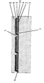
- the figure shows a schematical cross-section of an embodiment of the battery.
- the nanoporous photoelectrodes 4 are applied on a transparent conducting substrate 1, as in the original version of the dye-sensitized solar cell [Journal of the American Chemical Society, vol. 115 (1993) pp. 6382-6390], each on a predetermined area of the conducting coating 2. These areas form parallel strips of the required width for each solar cell separated by narrow insulating lines 3, where the conducting coating 2 of the substrate 1 has been removed.
- the photoelectrodes 4 are applied in such a way that each extends slightly over one edge of the corresponding conducting coating 2, while leaving bare the opposite edge.
- the photoelectrodes 4 are then covered with a porous layer of an electrical insulator 5.
- This layer is required to prevent short-circuiting in cases where the material of the counterelectrodes 6 would form ohmic contact with the photoelectrodes 4.
- the insulating layers 5 may at the same time act as a diffuse reflector that reflects light which has not yet been absorbed back into the photoelectrodes 4.
- Porous counterelectrodes 6 of any convenient electronically conducting material are now applied over the bare edge of each conducting strip 2 and the adjacent photoelectrode 4, thereby connecting the solar cells in series.
- the gaps 7 between the counterelectrodes 6 may be filled with a nonporous insulator to prevent electrical shunting through the electrolyte.
- the coatings 4 to 6 may be heat treated at any stage in order to remove undesired additives and make good electrical contacts by sintering.
- the sensitizing dye is then adsorbed through the porous counterelectrodes 6 and insulating layers 5 onto the nanoporous photoelectrodes 4. Finally the pores of layers 4 to 6 are filled with the electrolyte.
- the solar cell module is sealed by a top-cover 8, to prevent evaporation of the electrolyte and intrusion of humidity or oxygen.
- the top-cover 8 may at the same time serve to fill the gaps 7 between the counterelectrodes 6. Contacts are made at the first counterelectrode 9 and the last photoelectrode 10 of the series-connection.
- This new design of the dye-sensitized solar cell has the following advantages:
- the transparent conducting layer 2 e.g. fluorine doped tin oxide, tin doped indium oxide
- the insulating substrate 1 e.g. glass, plastic
- the transparent conducting layer 2 is scratched, etched or laser scribed in parallel lines 3 of the required separation (about 1 cm) in order to remove the conducting coating 2, thereby defining the area of each cell.
- a dispersion of nanocrystalline semiconductor powder e.g. titanium dioxide
- is applied e.g. by gravure printing or screen printing through a mask of appropriate geometry
- the photoelectrodes 4 (ca. 10 ⁇ m thick), each extending slightly over one edge of the corresponding conducting coating 2, while leaving bare the opposite edge.
- the photoelectrodes 4 may also be deposited over the whole surface first, e. g. by doctor blading, printing or spraying, and separated into parallel stripes subsequently, e. g. by mechanical, airjet, waterjet or laser scribing. This patterning may also be carried out after deposition of the insulating layers 5, by removing simultaneously the layers 4 and 5 at the required places.
- a dispersion of an insulator powder (e.g. glass or ceramics, such as aluminum oxide, silicon dioxide, titanium dioxide, zirconium dioxide) is now applied over the photoelectrodes 4 to create the porous insulating layers 5 (about 10 ⁇ m thick).
- an insulator powder e.g. glass or ceramics, such as aluminum oxide, silicon dioxide, titanium dioxide, zirconium dioxide
- the insulating layers 5 should contain particles of high refractive index (e.g. the rutile modification of titanium dioxide) and the appropriate size for strong light scattering (about 0,3 ⁇ m diameter in case of rutile).
- a binder that sinters at the temperature of heat treatment (below 550°C) may be required for the formation of well coherent and adherent layers 5.
- the binder may at the same time serve as insulator between the particles.
- the layers 5 may be obtained from a dispersion of rutile powder with a mean particle size around 0.3 ⁇ m and about 10% of its weight nanocrystalline zirconium dioxide powder with a particle size below 20 nm, which sinters on heat treatment below 550°C and forms a well insulating binder between the rutile particles.
- the rutile particles may be coated with a thin (several nanometer thick) film of an insulator (a low melting glass, silicon dioxide, aluminum dioxide, boron oxide, zirconium dioxide or a combination of these), which sinters on heat treatment below 550°C.
- the patterning of the insulating layers 5 may be achieved as described for the photoelectrodes 4 by techniques such as gravure printing or screen printing, or by mechanical, airjet, waterjet or laser scribing.
- a dispersion of a metal powder e.g. a platinum group metal, titanium, tungsten, molybdenum, chromium), graphite powder, carbon black, a conducting ceramic powder (e.g. fluorine doped tin oxide or tin doped indium oxide), optionally with a catalytic deposit of a platinum group metal, or a conducting polymer (e.g. polyaniline, polypyrrole, polythiophene) is applied for the counterelectrodes 6 (up to several 10 ⁇ m thick, depending on the required conductivity).
- a metal powder e.g. a platinum group metal, titanium, tungsten, molybdenum, chromium
- graphite powder e.g. fluorine doped tin oxide or tin doped indium oxide
- a conducting polymer e.g. polyaniline, polypyrrole, polythiophene
- Graphite powder has proven a good choice, because it combines sufficient conductivity and heat resistance as well as corrosion resistance and electrocatalytic activity with respect to the redox electrolyte.
- Graphite powder consists of platelike crystals which, on deposition from a liquid dispersion and drying, will preferentially align in the plane of the counterelectrodes 6, resulting in a high conductivity in this plane.
- the catalytic activity of the counterelectrodes 6 for reduction of the redox electrolyte as well as their conductivity may be considerably enhanced by adding about 20% of carbon black to the dispersion of graphite powder.
- the enhanced catalytic activity is due to the very high surface area of carbon black, while the improved conductivity results from the partial filling of large pores between the graphite flakes with smaller carbon black aggregates.
- photoelectrodes 4 patterning of the counterelectrodes 6 may be achieved by techniques such as gravure printing or screen printing through an appropriate mask or by mechanical, airjet, waterjet or laser scribing.
- the gaps 7 may be filled with a nonporous insulator (e.g. silicone rubber, a low melting glass frit or an organic polymer) to insulate adjacent counterelectrodes 6 from each other.
- a nonporous insulator e.g. silicone rubber, a low melting glass frit or an organic polymer
- Such an insulation is not necessary if just the pores of the coatings 4 to 6 are filled with electrolyte by capillary action later, such that the gaps 7 remain filled with air, nitrogen or another gas.
- the coatings 4 to 6 are heat treated at any stage to remove solvents and other undesired additives and to improve their mechanical strength and electrical properties by sintering.
- the coated substrate 1 is dipped into a dye solution to sensitize the photoelectrodes 4. After drying electrolyte is admitted in order to fill the pores of layers 4 to 6 by capillary action.
- the module is encapsulated with a top-cover 8 (e.g. glass, organic polymer, anodized aluminum, lacquer or any other insulator).
- the top-cover 8 may also, if necessary, serve to fill the gaps 7 between the counterelectrodes 6. Electrical contacts are made at the first counterelectrode 9 and the last photoelectrode 10 of the series-connected module.
Landscapes
- Engineering & Computer Science (AREA)
- Power Engineering (AREA)
- Microelectronics & Electronic Packaging (AREA)
- Chemical & Material Sciences (AREA)
- Chemical Kinetics & Catalysis (AREA)
- Electrochemistry (AREA)
- Hybrid Cells (AREA)
- Photovoltaic Devices (AREA)
Abstract
Description
- This invention concerns monolithic, series-connected, dye-sensitized photovoltaic modules consisting of dye-sensitized nanoporous semiconductor layers as photoelectrodes on an electrically conducting, transparent substrate, an electron transferring redox electrolyte and counterelectrodes. Single photovoltaic cells of this type have already been described [Journal of the American Chemical Society, vol. 115 (1993) pp. 6382-6390]. Tin oxide coated glass as transparent, electrically conducting substrate is covered with a porous semiconductor layer of nanocrystalline titanium dioxide as photoelectrode and sensitized for visible light by adsorption of a dye. The dye is excited by absorption of light and injects an electron into the titanium dioxide. Through the conducting substrate the electrons reach the external circuit where they may carry out electrical work. The oxidized dye is reduced by the electron transferring electrolyte, which fills the pores of photoelectrode and the space up to the counterelectrode. The counterelectrode usually consists of tin oxide coated glass as well, which is catalytically activated with platinum in order to transfer the electrons arriving from the external circuit back to the electrolyte.
- The fabrication of efficient large surface area cells was difficult up to now since the distance between photo- and counterelectrode soon becomes too large (> 20 µm) due to the limited flatness of the separate substrates, causing additional ohmic losses and even diffusion limitations of the photocurrent in the electrolyte layer. Moreover the conductivity of the substrate is not sufficient to carry the high photocurrents produced by a large surface area cell. A possible solution would be the series-connection of many narrow stripes of cells to a module, by connecting the counterelectrode of one cell to the photoelectrode of the adjacent cell, as known from amorphous silicon cells [Solar Energy, vol 23 (1979) pp. 145-147]. However, with the present design of the dye-sensitized photovoltaic cell this would require conducting bridges reaching from one substrate through the electrolyte to the other substrate, while the distance between the substrates has to be kept very small (< 20 µm). The corrosiveness of the electrolyte leaves little choice of suitable materials for these interconnecting bridges. Also the formation of lines of electrical contacts between the two separate substrates at temperatures which do not destroy the sensitizing dye is difficult to achieve.
- DE-A-4 225 576 describes a photovoltaic cell wherein series-connected elements are arranged as parallel elongated strips on a common electrically insulating transparent substrate.
- In this invention we present a new design of the dye-sensitized solar cell, which allows to fabricate large surface area photovoltaic modules by series-connecting many photo- and counterelectrodes on the same substrate.
- To this effect the present invention concerns a battery of photovoltaic cells as specified in
claim 1. Particularly useful embodiments of the battery are specified independant claims 2 to 13. The invention also concerns a process for manufacturing the battery as specified in claim 14. - Particularly useful execution forms of the process are specified in dependant claims 15 to 20.
- The figure shows a schematical cross-section of an embodiment of the battery.
- The nanoporous photoelectrodes 4 are applied on a transparent conducting
substrate 1, as in the original version of the dye-sensitized solar cell [Journal of the American Chemical Society, vol. 115 (1993) pp. 6382-6390], each on a predetermined area of the conductingcoating 2. These areas form parallel strips of the required width for each solar cell separated by narrowinsulating lines 3, where the conductingcoating 2 of thesubstrate 1 has been removed. The photoelectrodes 4 are applied in such a way that each extends slightly over one edge of the corresponding conductingcoating 2, while leaving bare the opposite edge. The photoelectrodes 4 are then covered with a porous layer of anelectrical insulator 5. This layer is required to prevent short-circuiting in cases where the material of thecounterelectrodes 6 would form ohmic contact with the photoelectrodes 4. Theinsulating layers 5 may at the same time act as a diffuse reflector that reflects light which has not yet been absorbed back into the photoelectrodes 4. -
Porous counterelectrodes 6 of any convenient electronically conducting material are now applied over the bare edge of each conductingstrip 2 and the adjacent photoelectrode 4, thereby connecting the solar cells in series. The gaps 7 between thecounterelectrodes 6 may be filled with a nonporous insulator to prevent electrical shunting through the electrolyte. The coatings 4 to 6 may be heat treated at any stage in order to remove undesired additives and make good electrical contacts by sintering. - The sensitizing dye is then adsorbed through the
porous counterelectrodes 6 and insulatinglayers 5 onto the nanoporous photoelectrodes 4. Finally the pores of layers 4 to 6 are filled with the electrolyte. The solar cell module is sealed by a top-cover 8, to prevent evaporation of the electrolyte and intrusion of humidity or oxygen. The top-cover 8 may at the same time serve to fill the gaps 7 between thecounterelectrodes 6. Contacts are made at thefirst counterelectrode 9 and the last photoelectrode 10 of the series-connection. - This new design of the dye-sensitized solar cell has the following advantages:
- 1. Only a single transparent conducting
substrate 1 is required, which reduces significantly the materials costs of the solar cell. - 2. Both photoelectrodes 4 and
counterelectrodes 6 are deposited on top of one another on the same substrate. Their separation is thus minimized independent of the flatness of the substrate. - 3. The
insulating layers 5 act as diffuse reflectors immediately on top of the photoelectrodes 4, and thus improve the efficiency of the solar cell. - 4. The electrolyte is fixed by capillary forces in the porous matrix of coatings 4 to 6 and does not constitute an additional, free flowing layer.
- 5. The
counterelectrodes 6 have an enlarged surface area due to their porosity, resulting in a higher catalytic efficiency for electron exchange with the electrolyte. - 6. The series-connection of many solar cells on a single
substrate in "Z"-configuration is achieved, as in the case
of amorphous silicon cells [Solar Energy, vol 23 (1979) pp.
145-147], by simple overlap of the
counterelectrodes 6 with theback contacts 2 of the adjacent photoelectrodes 4. - 7. The pattern of the layers 4 to 6 may be produced on a large scale by common printing techniques, such as gravure printing or screen printing. The layers 4 to 6 may also be deposited over the whole surface first and be patterned subsequently, e. g. by mechanical, airjet, waterjet or laser scribing.
- 8. The layers 4 to 6 may be produced in a continuous process
immediately following fabrication of the
glass substrate 1 and coating with the transparent conductinglayer 2 by successive deposition, patterning and heat treatment of the layers 4 to 6 on thesubstrate 1, which is transported continuously in the sense of thelines 3 through the different production stages. - 9. The porosity of the
insulating layers 5 and thecounterelectrodes 6 allows application of the heat and humidity sensitive dye and electrolyte after fabrication of the layers 4 to 6 and formation of the electrical interconnections. - 10.The top-
cover 8 only serves to seal and insulate the cell but has not any electrical conductor function. -
- The transparent conducting layer 2 (e.g. fluorine doped tin oxide, tin doped indium oxide) on the insulating substrate 1 (e.g. glass, plastic) is scratched, etched or laser scribed in
parallel lines 3 of the required separation (about 1 cm) in order to remove the conductingcoating 2, thereby defining the area of each cell. - A dispersion of nanocrystalline semiconductor powder (e.g. titanium dioxide) is applied (e.g. by gravure printing or screen printing through a mask of appropriate geometry) to deposit the photoelectrodes 4 (ca. 10 µm thick), each extending slightly over one edge of the corresponding conducting
coating 2, while leaving bare the opposite edge. The photoelectrodes 4 may also be deposited over the whole surface first, e. g. by doctor blading, printing or spraying, and separated into parallel stripes subsequently, e. g. by mechanical, airjet, waterjet or laser scribing. This patterning may also be carried out after deposition of theinsulating layers 5, by removing simultaneously thelayers 4 and 5 at the required places. - A dispersion of an insulator powder (e.g. glass or ceramics, such as aluminum oxide, silicon dioxide, titanium dioxide, zirconium dioxide) is now applied over the photoelectrodes 4 to create the porous insulating layers 5 (about 10 µm thick). In order to reflect light that has not been absorbed by the photoelectrodes 4 back into the same and thus enhance the efficiency of the solar cell the
insulating layers 5 should contain particles of high refractive index (e.g. the rutile modification of titanium dioxide) and the appropriate size for strong light scattering (about 0,3 µm diameter in case of rutile). The addition of a binder that sinters at the temperature of heat treatment (below 550°C) may be required for the formation of well coherent andadherent layers 5. In case of poorly insulating light scattering particles, such as rutile, the binder may at the same time serve as insulator between the particles. - For example the
layers 5 may be obtained from a dispersion of rutile powder with a mean particle size around 0.3 µm and about 10% of its weight nanocrystalline zirconium dioxide powder with a particle size below 20 nm, which sinters on heat treatment below 550°C and forms a well insulating binder between the rutile particles. Alternatively the rutile particles may be coated with a thin (several nanometer thick) film of an insulator (a low melting glass, silicon dioxide, aluminum dioxide, boron oxide, zirconium dioxide or a combination of these), which sinters on heat treatment below 550°C. - The patterning of the insulating
layers 5 may be achieved as described for the photoelectrodes 4 by techniques such as gravure printing or screen printing, or by mechanical, airjet, waterjet or laser scribing. - A dispersion of a metal powder (e.g. a platinum group metal, titanium, tungsten, molybdenum, chromium), graphite powder, carbon black, a conducting ceramic powder (e.g. fluorine doped tin oxide or tin doped indium oxide), optionally with a catalytic deposit of a platinum group metal, or a conducting polymer (e.g. polyaniline, polypyrrole, polythiophene) is applied for the counterelectrodes 6 (up to several 10 µm thick, depending on the required conductivity).
- Graphite powder has proven a good choice, because it combines sufficient conductivity and heat resistance as well as corrosion resistance and electrocatalytic activity with respect to the redox electrolyte. Graphite powder consists of platelike crystals which, on deposition from a liquid dispersion and drying, will preferentially align in the plane of the
counterelectrodes 6, resulting in a high conductivity in this plane. - The catalytic activity of the
counterelectrodes 6 for reduction of the redox electrolyte as well as their conductivity may be considerably enhanced by adding about 20% of carbon black to the dispersion of graphite powder. The enhanced catalytic activity is due to the very high surface area of carbon black, while the improved conductivity results from the partial filling of large pores between the graphite flakes with smaller carbon black aggregates. - Again a binder is required for good cohesion and adhesion of the
counterelectrodes 6. Thus, nanocrystalline titanium dioxide with a particle size below 20 nm added to the dispersion at a weight of 15% of the graphite powder sinters on heating below 550°C and yields well adherent, scratchresistant counter electrodes 6 with a sheet resistance of less than 10 Ohms for a thickness of 30 µm. - As described for the photoelectrodes 4 patterning of the
counterelectrodes 6 may be achieved by techniques such as gravure printing or screen printing through an appropriate mask or by mechanical, airjet, waterjet or laser scribing. - The gaps 7 may be filled with a nonporous insulator (e.g. silicone rubber, a low melting glass frit or an organic polymer) to insulate
adjacent counterelectrodes 6 from each other. Such an insulation is not necessary if just the pores of the coatings 4 to 6 are filled with electrolyte by capillary action later, such that the gaps 7 remain filled with air, nitrogen or another gas. If necessary the coatings 4 to 6 are heat treated at any stage to remove solvents and other undesired additives and to improve their mechanical strength and electrical properties by sintering. - The
coated substrate 1 is dipped into a dye solution to sensitize the photoelectrodes 4. After drying electrolyte is admitted in order to fill the pores of layers 4 to 6 by capillary action. The module is encapsulated with a top-cover 8 (e.g. glass, organic polymer, anodized aluminum, lacquer or any other insulator). The top-cover 8 may also, if necessary, serve to fill the gaps 7 between thecounterelectrodes 6. Electrical contacts are made at thefirst counterelectrode 9 and the last photoelectrode 10 of the series-connected module.
Claims (20)
- A battery of photovoltaic cells, which consists of a monolithic assembly of a plurality of series-connected photovoltaic elements arranged as parallel elongated stripes on a common electrically insulating transparent substrate (1), each said element comprising a dye-sensitized photoanode made of a porous layer (4) of a polycrystalline semiconductor, a counterelectrode made of a porous layer (6) of an electrically conducting material, separated from said photoanode by an intermediate porous layer (5) of an electrically insulating material, wherein the pores of said layers (4, 5, 6) are at least partially filled with an electron transferring electrolyte, and an intermediate layer (2) of a transparent electrically conducting material interposed between the substrate (1) and the layer (4) constituting the photoanode of each said element, the respective electrically conducting intermediate layers (2) of two adjacent elements being separated from each other by a continuous elongated gap (3) and the layer (6) constituting the counterelectrode of the first element of the series being electrically connected with a first terminal (9) of the battery while the layers (6) of the counterelectrodes of the other elements are electrically connected, over said gap (3), with the intermediate electrically conducting layer (2) of an adjacent element while being electrically insulated from each other and the electrically conducting intermediate layer (2) of the last element of the series being electrically connected with a second terminal (10) of the battery, and said assembly being covered with an electrically insulating liquid-tight top-cover (8).
- A battery according to claim 1, characterized in that said intermediate porous layer (5) of electrically insulating material is made of fine particles of a glass or ceramic material.
- A battery according to claim 2, characterized in that said material is constituted of at least one of the following metal oxides: aluminum oxide, silicon dioxide, titanium dioxide, and zirconium dioxide.
- A battery according to claim 2 or 3, characterized in that said intermediate porous layer (5) is at least partially made of at least one material having a high refractive index in the form of particles with a size appropriate for imparting them strong light scattering properties.
- A battery according to claim 4, characterized in that said material is titanium dioxide, as rutile, wherein the size of said particles is of the order of 0.3 micrometers.
- A battery according to claim 4 or 5, characterized in that said intermediate porous layer (5) is made of a mixture of a major amount of said material of high refractive index with a minor amount of an electrically insulating material, in the form of particles having a size appropriate for imparting them the property of sintering at a temperature below 550°C.
- A battery according to claim 6, characterized in that said electrically insulating material is selected from a low melting glass or at least one of the following metal oxides: silicon dioxide, aluminum dioxide, boron dioxide, zirconium dioxide or a combination of at least two of these oxides.
- A battery according to claim 4 or 5, characterized in that at least some of said particles of high refractive index material are coated with a film of an electrically insulating material, wherein said film has the property of sintering at a temperature below 550°C.
- A battery according to claim 1, characterized in that said porous layer (6) of electrically conducting material is made from a material selected from at least one metal powder, at least one electrically conducting ceramic powder, powdered graphite, powdered carbon black, at least one electrically conducting organic polymer, and mixtures thereof.
- A battery according to claim 9, characterized in that said metal is selected from a platinum group metal or at least one of the following metals: titanium, tungsten, molybdenum and chromium, said electrically conducting ceramic material is selected from tin oxide doped with fluorine or antimony, indium oxide doped with tin, and said electrically conducting organic polymer is a polymer on the basis of polyaniline, polypyrrole or polythiophene, wherein a catalytic deposit of a platinum group metal covers at least the electrochemically active surface of the counterelectrode constituted by said porous layer (6).
- A battery according to claim 10, characterized in that said porous layer (6) of electrically conducting material is made of a mixture of powdered graphite, carbon black and at least one binder material in the form of particles having a size appropriate for imparting them the property of sintering at a temperature below 550°C.
- A battery according to claim 11, characterized in that said binder material is titanium dioxide with a particle size of less than 20 nanometers.
- A battery according to claim 11 or 12, characterized in that said porous layer (6) is made of about 65 % by weight graphite powder, 20 % by weight carbon black and 15 % by weight titanium dioxide.
- A process for manufacturing a battery of photovoltaic cells according to claim 1, which comprises the following steps:a) forming, on the surface of an electrically insulating transparent substrate (1), a plurality of parallel stripes (2) of a transparent electrically conducting material, said stripes (2) being separated from each other by a continuous elongated gap (3) of bare surface of substrate (1);b) covering each of said stripes (2) with a porous layer (4) of a polycrystalline semiconductor;c) covering said porous layer (4) with a porous layer (5) of an insulating material, the three above-indicated steps a), b) and c) being carried out so that the said porous layers (4) and (5) cover the exposed area of surface of said substrate (1) in the elongated gap (3) along one edge of said stripe (2) of electrically conducting material while leaving bare at least a portion of the surface of said stripe (2) along the opposite edge thereof;d) covering said porous layer (5) of insulating material with a porous layer (6) of electrically conducting material, so that said latter layer (6) overlaps said former layer (5) over the portion thereof covering said gap (3) and contacts the bare portion of the surface of the adjacent stripe (2) of electrically conducting material while leaving a gap (7) on the opposite edge thus forming an assembly of a plurality of series-connected elements;e) contacting said assembly with a liquid solution of a dye-sensitizer, so that this solution is introduced into the porous layer (4) of semiconductor of each element, through the porous layer (6) of electrically conducting material and the porous layer (5) of electrically insulating material;f) evaporating the solvent of said solution of dye-sensitizer, leaving the dye adsorbed on the layer (4) of semiconductor;g) contacting the assembly with a liquid electrolyte, so that this electrolyte fills the pores of said porous layers (6, 5 and 4); andh) forming electrical first and second connections (9, 10) to the battery terminals, said first connection (9) being electrically connected with the porous layer (6) of conducting material of the first element of the battery and said second connection (10) being electrically connected with the stripe (2) of electrically conducting material of the last element, and covering the thus obtained assembly with an electrically insulating liquid-tight top-cover (8).
- A process according to claim 14, characterized in that steps e), f) and g) are combined together by using a solution of a dye-sensitizer in a liquid electrolyte.
- A process according to claim 14 or 15, characterized in that it further comprises the step of:i) electrically insulating from one another the porous layers (6) of electrically conducting material of all the elements by filling the gaps (7) separating these layers (6) with a liquid-tight insulating material, said step i) being optionally combined with the final operation of step h).
- A process according to claim 14 or 15, characterized in that the step g) of contacting the assembly with a liquid electrolyte is carried out in such a manner that the inner cavities of the porous layers (4, 5, 6) are filled with electrolyte by capillarity, and in that an insulating gas, such as air or nitrogen, is left in the gaps (7) separating the porous layers (6) constituting the counterelectrode.
- A process according to claim 14 or 15, characterized in that the steps b), c) and d) are carried out by suitable printing techniques in order to deposit the porous layers (4, 5 and 6) of semiconductor, insulating material and electrically conducting material, respectively, in the required pattern of parallel stripes on the substrate (1).
- A process according to claim 14 or 15, characterized in that the steps a), b), c) and d) are carried out by first applying a layer (2) of transparent electrically conducting material onto the whole surface of the substrate (1), then removing this layer (2) at the appropriate places to form the gaps (3), then applying the porous layers (4 and 5) of semiconductor and insulating material over the whole surface of the such coated substrate (1), then removing these layers (4 and 5) at the appropriate places to expose one edge of each stripe (2) of transparent electrically conducting material, then applying a layer (6) of porous electrically conducting material onto the whole surface of the such coated substrate (1), then removing this layer (6), optionally together with the underlying porous layers (4 and 5), at the appropriate places to form the gaps (7).
- A process according to claim 18 or 19, characterized in that the elongated gaps (3) and the porous layers (4, 5, 6) are fabricated in a continuous process by successive patterning of the layer (2) of transparent electrically conducting material and deposition, patterning and heat treatment of the layer (4) constituting the photoanodes, the layer (5) of insulating material and the layer (6) of electrically conducting material, on the substrate (1) while continuously transporting the latter along the length of the elongated gaps (3), through a plurality of working stations.
Applications Claiming Priority (1)
| Application Number | Priority Date | Filing Date | Title |
|---|---|---|---|
| PCT/IB1995/000936 WO1997016838A1 (en) | 1995-10-31 | 1995-10-31 | A battery of photovoltaic cells and process for manufacturing the same |
Publications (2)
| Publication Number | Publication Date |
|---|---|
| EP0858669A1 EP0858669A1 (en) | 1998-08-19 |
| EP0858669B1 true EP0858669B1 (en) | 1999-11-03 |
Family
ID=11004384
Family Applications (1)
| Application Number | Title | Priority Date | Filing Date |
|---|---|---|---|
| EP95934259A Expired - Lifetime EP0858669B1 (en) | 1995-10-31 | 1995-10-31 | A battery of photovoltaic cells and process for manufacturing the same |
Country Status (6)
| Country | Link |
|---|---|
| US (1) | US6069313A (en) |
| EP (1) | EP0858669B1 (en) |
| JP (1) | JP4087445B2 (en) |
| AU (1) | AU728725B2 (en) |
| DE (1) | DE69513203T2 (en) |
| WO (1) | WO1997016838A1 (en) |
Cited By (1)
| Publication number | Priority date | Publication date | Assignee | Title |
|---|---|---|---|---|
| DE10249246B4 (en) * | 2002-10-23 | 2013-01-17 | Fraunhofer-Gesellschaft zur Förderung der angewandten Forschung e.V. | Dye-sensitized photovoltaic cell, a process for producing these photovoltaic cells and their use |
Families Citing this family (158)
| Publication number | Priority date | Publication date | Assignee | Title |
|---|---|---|---|---|
| AUPP931799A0 (en) * | 1999-03-18 | 1999-04-15 | Sustainable Technologies Australia Limited | Methods to implement interconnects in multi-cell regenerative photovoltaic photoelectrochemical devices |
| AUPP953999A0 (en) * | 1999-03-30 | 1999-04-29 | Sustainable Technologies Australia Limited | Methods to manufacture single cell and multi-cell regenerative photoelectrochemical devices |
| JP4414036B2 (en) * | 1999-12-27 | 2010-02-10 | シャープ株式会社 | Method for producing dye-sensitized solar cell |
| US6305073B1 (en) | 1999-12-29 | 2001-10-23 | Gm Nameplate, Inc. | One-sided electrode arrangement on an intermediate spacer for a touchscreen |
| US7205473B2 (en) * | 2002-01-25 | 2007-04-17 | Konarka Technologies, Inc. | Photovoltaic powered multimedia greeting cards and smart cards |
| US6706963B2 (en) * | 2002-01-25 | 2004-03-16 | Konarka Technologies, Inc. | Photovoltaic cell interconnection |
| US20030192584A1 (en) * | 2002-01-25 | 2003-10-16 | Konarka Technologies, Inc. | Flexible photovoltaic cells and modules formed using foils |
| US6913713B2 (en) | 2002-01-25 | 2005-07-05 | Konarka Technologies, Inc. | Photovoltaic fibers |
| US6949400B2 (en) * | 2002-01-25 | 2005-09-27 | Konarka Technologies, Inc. | Ultrasonic slitting of photovoltaic cells and modules |
| US7414188B2 (en) * | 2002-01-25 | 2008-08-19 | Konarka Technologies, Inc. | Co-sensitizers for dye sensitized solar cells |
| US7186911B2 (en) * | 2002-01-25 | 2007-03-06 | Konarka Technologies, Inc. | Methods of scoring for fabricating interconnected photovoltaic cells |
| US6900382B2 (en) * | 2002-01-25 | 2005-05-31 | Konarka Technologies, Inc. | Gel electrolytes for dye sensitized solar cells |
| US20050284513A1 (en) * | 2002-08-08 | 2005-12-29 | Christoph Brabec | Chip card comprising an integrated energy converter |
| US7586035B2 (en) * | 2004-02-19 | 2009-09-08 | Konarka Technologies, Inc. | Photovoltaic cell with spacers |
| US20030192585A1 (en) * | 2002-01-25 | 2003-10-16 | Konarka Technologies, Inc. | Photovoltaic cells incorporating rigid substrates |
| US6919119B2 (en) * | 2000-05-30 | 2005-07-19 | The Penn State Research Foundation | Electronic and opto-electronic devices fabricated from nanostructured high surface to volume ratio thin films |
| SE521683C2 (en) * | 2000-06-14 | 2003-11-25 | Ivf Industriforskning Och Utve | Method of Manufacture of Sealed Monolithic Electrochemical Systems and Sealed Monolithic Electrochemical System |
| AUPR174800A0 (en) * | 2000-11-29 | 2000-12-21 | Australian National University, The | Semiconductor processing |
| US20040074531A1 (en) * | 2000-12-26 | 2004-04-22 | Fumio Matsui | Solar cell |
| DE10120579C2 (en) * | 2001-04-26 | 2003-06-26 | Siemens Ag | Highly sensitive moisture indicator for thin film technology |
| DE10297633T5 (en) * | 2002-01-04 | 2005-05-19 | Gt Equipment Technologies Inc. | Solarzellenaufreihungsmaschine |
| CA2474491A1 (en) * | 2002-01-25 | 2003-08-07 | Bill Beckenbaugh | Structures and materials for dye sensitized solar cells |
| WO2003065393A2 (en) * | 2002-01-25 | 2003-08-07 | Konarka Technologies, Inc. | Displays with integrated photovoltaic cells |
| CA2474494A1 (en) * | 2002-01-25 | 2003-08-07 | Savvas E. Hadjikyriacou | Photovoltaic cell components and materials |
| JP4392741B2 (en) * | 2002-04-17 | 2010-01-06 | 日揮触媒化成株式会社 | Photoelectric cell |
| AU2003271105A1 (en) * | 2002-10-15 | 2004-05-04 | Sharp Kabushiki Kaisha | Sensitized dye solar cell and sensitized dye solar cell module |
| JP4161688B2 (en) * | 2002-11-18 | 2008-10-08 | アイシン精機株式会社 | Wet solar cell |
| US9079246B2 (en) | 2009-12-08 | 2015-07-14 | Baker Hughes Incorporated | Method of making a nanomatrix powder metal compact |
| US9682425B2 (en) | 2009-12-08 | 2017-06-20 | Baker Hughes Incorporated | Coated metallic powder and method of making the same |
| US8403037B2 (en) * | 2009-12-08 | 2013-03-26 | Baker Hughes Incorporated | Dissolvable tool and method |
| US8327931B2 (en) * | 2009-12-08 | 2012-12-11 | Baker Hughes Incorporated | Multi-component disappearing tripping ball and method for making the same |
| US8297364B2 (en) | 2009-12-08 | 2012-10-30 | Baker Hughes Incorporated | Telescopic unit with dissolvable barrier |
| US9109429B2 (en) | 2002-12-08 | 2015-08-18 | Baker Hughes Incorporated | Engineered powder compact composite material |
| US9101978B2 (en) | 2002-12-08 | 2015-08-11 | Baker Hughes Incorporated | Nanomatrix powder metal compact |
| US7078613B2 (en) * | 2002-12-11 | 2006-07-18 | General Electric Company | Structured micro-channel semiconductor electrode for photovoltaic cells |
| US8586861B2 (en) * | 2003-01-12 | 2013-11-19 | 3Gsolar Photovoltaics Ltd. | Solar cell device |
| WO2009069129A2 (en) * | 2007-11-27 | 2009-06-04 | 3Gsolar Ltd. | Large area dye cells, and methods of production thereof |
| IL153895A (en) * | 2003-01-12 | 2013-01-31 | Orion Solar Systems Ltd | Solar cell device |
| US7170001B2 (en) * | 2003-06-26 | 2007-01-30 | Advent Solar, Inc. | Fabrication of back-contacted silicon solar cells using thermomigration to create conductive vias |
| US7649141B2 (en) * | 2003-06-30 | 2010-01-19 | Advent Solar, Inc. | Emitter wrap-through back contact solar cells on thin silicon wafers |
| JP2005158470A (en) * | 2003-11-25 | 2005-06-16 | Ngk Spark Plug Co Ltd | Dye-sensitized solar cell |
| JP3717506B2 (en) | 2004-01-20 | 2005-11-16 | シャープ株式会社 | Dye-sensitized solar cell module |
| US20050172996A1 (en) * | 2004-02-05 | 2005-08-11 | Advent Solar, Inc. | Contact fabrication of emitter wrap-through back contact silicon solar cells |
| US20060060238A1 (en) * | 2004-02-05 | 2006-03-23 | Advent Solar, Inc. | Process and fabrication methods for emitter wrap through back contact solar cells |
| US7335555B2 (en) * | 2004-02-05 | 2008-02-26 | Advent Solar, Inc. | Buried-contact solar cells with self-doping contacts |
| US7144751B2 (en) * | 2004-02-05 | 2006-12-05 | Advent Solar, Inc. | Back-contact solar cells and methods for fabrication |
| US7829781B2 (en) * | 2004-06-01 | 2010-11-09 | Konarka Technologies, Inc. | Photovoltaic module architecture |
| JP4063802B2 (en) * | 2004-08-04 | 2008-03-19 | シャープ株式会社 | Photoelectrode |
| CN101002292A (en) * | 2004-08-11 | 2007-07-18 | 戴索有限公司 | Photoelectrochemical photovoltaic panel and method to manufacture thereof |
| AU2005270739B2 (en) * | 2004-08-11 | 2009-12-24 | Dyesol Ltd | Photoelectrochemical Photovoltaic Panel and method to manufacture thereof |
| US8309843B2 (en) * | 2004-08-19 | 2012-11-13 | Banpil Photonics, Inc. | Photovoltaic cells based on nanoscale structures |
| JP2009506360A (en) * | 2005-08-22 | 2009-02-12 | コナルカ テクノロジーズ インコーポレイテッド | Display with built-in photovoltaic cell |
| US20070079867A1 (en) * | 2005-10-12 | 2007-04-12 | Kethinni Chittibabu | Photovoltaic fibers |
| US8314327B2 (en) * | 2005-11-06 | 2012-11-20 | Banpil Photonics, Inc. | Photovoltaic cells based on nano or micro-scale structures |
| GB2432723B (en) * | 2005-11-25 | 2010-12-08 | Seiko Epson Corp | Electrochemical cell and method of manufacture |
| GB2432722A (en) * | 2005-11-25 | 2007-05-30 | Seiko Epson Corp | Electrochemical cell and method of manufacture |
| GB2432721B (en) * | 2005-11-25 | 2011-06-22 | Seiko Epson Corp | Electrochemical cell structure and method of fabrication |
| US20070125419A1 (en) * | 2005-12-01 | 2007-06-07 | Gui John Y | Dye sensitized solar cells having blocking layers and methods of manufacturing the same |
| JP4523549B2 (en) | 2006-01-18 | 2010-08-11 | シャープ株式会社 | Dye-sensitized solar cell and dye-sensitized solar cell module |
| TWI346406B (en) * | 2006-02-16 | 2011-08-01 | Lg Chemical Ltd | Lithium secondary battery with enhanced heat-resistance |
| EP1840916A1 (en) | 2006-03-27 | 2007-10-03 | IVF Industriforskning och Utveckling AB | A sealed monolithic photo-electrochemical system and a method for manufacturing a sealed monolithic photo-electrochemical system |
| JP5140588B2 (en) | 2006-07-06 | 2013-02-06 | シャープ株式会社 | Dye-sensitized solar cell module and manufacturing method thereof |
| WO2008004553A1 (en) | 2006-07-06 | 2008-01-10 | Sharp Kabushiki Kaisha | Dye-sensitized solar cell module and method for fabricating same |
| CA2568136C (en) * | 2006-11-30 | 2008-07-29 | Tenxc Wireless Inc. | Butler matrix implementation |
| EP1936644A3 (en) * | 2006-12-22 | 2011-01-05 | Sony Deutschland Gmbh | A photovoltaic cell |
| US20080216887A1 (en) * | 2006-12-22 | 2008-09-11 | Advent Solar, Inc. | Interconnect Technologies for Back Contact Solar Cells and Modules |
| WO2009001343A2 (en) * | 2007-06-24 | 2008-12-31 | 3Gsolar Ltd. | Dry cell having a sintered cathode layer |
| WO2009053979A2 (en) * | 2007-10-24 | 2009-04-30 | 3Gsolar Ltd. | Monolithic dye cell assembly having reduced ion migration in intercell seals |
| KR101146768B1 (en) * | 2007-06-06 | 2012-05-21 | 가부시키가이샤후지쿠라 | Dye-sensitized solar battery module and method for manufacturing the same |
| JP4488034B2 (en) * | 2007-06-29 | 2010-06-23 | 株式会社日立製作所 | Dye-sensitized solar cell |
| JP2009110796A (en) * | 2007-10-30 | 2009-05-21 | Sony Corp | Dye-sensitized photoelectric conversion element module, manufacturing method thereof, and electronic apparatus |
| US20090126786A1 (en) * | 2007-11-13 | 2009-05-21 | Advent Solar, Inc. | Selective Emitter and Texture Processes for Back Contact Solar Cells |
| KR20090051597A (en) * | 2007-11-19 | 2009-05-22 | 한국전자통신연구원 | Dye-Sensitized Solar Cells Using Conductive Fiber Electrodes |
| EP2897144B1 (en) | 2007-12-12 | 2017-09-27 | Sharp Kabushiki Kaisha | Photosensitized solar cell module and production method thereof |
| JP2009146625A (en) * | 2007-12-12 | 2009-07-02 | Sony Corp | Dye-sensitized photoelectric conversion element module and manufacturing method thereof, photoelectric conversion element module and manufacturing method thereof, and electronic apparatus |
| GB2456166B (en) * | 2008-01-04 | 2012-01-25 | Pv Systems Ltd | A photovoltaic panel |
| EP2085986A1 (en) | 2008-01-30 | 2009-08-05 | Swerea IVF AB | A sealed monolithic electrochemical system |
| JP5351553B2 (en) * | 2008-04-28 | 2013-11-27 | 株式会社フジクラ | Photoelectric conversion element module |
| KR20110008284A (en) * | 2008-04-29 | 2011-01-26 | 어플라이드 머티어리얼스, 인코포레이티드 | Photovoltaic Modules Manufactured Using Monolithic Module Assembly Technologies |
| JP5273709B2 (en) | 2008-07-02 | 2013-08-28 | シャープ株式会社 | Dye-sensitized solar cell, method for producing the same, and dye-sensitized solar cell module |
| US20100006148A1 (en) * | 2008-07-08 | 2010-01-14 | Honeywell International Inc. | Solar cell with porous insulating layer |
| EP2316136A2 (en) * | 2008-08-29 | 2011-05-04 | Zylum Beteiligungsgesellschaft mbH & Co. Patente II KG | Layer system for solar absorber |
| TW201013947A (en) * | 2008-09-23 | 2010-04-01 | Tripod Technology Corp | Electrochemical device and method of fabricating the same |
| EP2348570A4 (en) * | 2008-10-17 | 2012-08-22 | Sharp Kk | Dye-sensitized solar cell and dye-sensitized solar cell module |
| US20120042930A1 (en) | 2009-04-15 | 2012-02-23 | Ryohsuke Yamanaka | Dye-sensitized solar cell and dye-sensitized solar cell module |
| JP4683396B2 (en) | 2009-04-30 | 2011-05-18 | シャープ株式会社 | Porous electrode, dye-sensitized solar cell, and dye-sensitized solar cell module |
| JP2010278405A (en) * | 2009-06-01 | 2010-12-09 | Smart Solar International Inc | Photovoltaic generation system and photovoltaic generation device |
| EP2312641A1 (en) * | 2009-10-13 | 2011-04-20 | Ecole Polytechnique Fédérale de Lausanne (EPFL) | Device comprising electrical contacts and its production process |
| JP5456054B2 (en) | 2009-11-02 | 2014-03-26 | シャープ株式会社 | Wet solar cell and wet solar cell module |
| US20110108102A1 (en) * | 2009-11-06 | 2011-05-12 | Honeywell International Inc. | Solar cell with enhanced efficiency |
| KR101108182B1 (en) * | 2009-12-01 | 2012-01-31 | 삼성에스디아이 주식회사 | Dye-Sensitized Solar Cell |
| US8528633B2 (en) | 2009-12-08 | 2013-09-10 | Baker Hughes Incorporated | Dissolvable tool and method |
| US10240419B2 (en) | 2009-12-08 | 2019-03-26 | Baker Hughes, A Ge Company, Llc | Downhole flow inhibition tool and method of unplugging a seat |
| US8425651B2 (en) | 2010-07-30 | 2013-04-23 | Baker Hughes Incorporated | Nanomatrix metal composite |
| US9127515B2 (en) | 2010-10-27 | 2015-09-08 | Baker Hughes Incorporated | Nanomatrix carbon composite |
| US8573295B2 (en) | 2010-11-16 | 2013-11-05 | Baker Hughes Incorporated | Plug and method of unplugging a seat |
| US9243475B2 (en) | 2009-12-08 | 2016-01-26 | Baker Hughes Incorporated | Extruded powder metal compact |
| US9227243B2 (en) | 2009-12-08 | 2016-01-05 | Baker Hughes Incorporated | Method of making a powder metal compact |
| JP4761327B2 (en) | 2010-01-12 | 2011-08-31 | シャープ株式会社 | Wet solar cell and wet solar cell module |
| JP5424259B2 (en) | 2010-02-02 | 2014-02-26 | シャープ株式会社 | Solar cell and solar cell module |
| US8424610B2 (en) | 2010-03-05 | 2013-04-23 | Baker Hughes Incorporated | Flow control arrangement and method |
| US9752932B2 (en) | 2010-03-10 | 2017-09-05 | Drexel University | Tunable electro-optic filter stack |
| JP4803305B2 (en) * | 2010-03-30 | 2011-10-26 | 大日本印刷株式会社 | Dye-sensitized solar cell |
| WO2011155441A1 (en) | 2010-06-09 | 2011-12-15 | シャープ株式会社 | Wet-type solar cell and wet-type solar cell module |
| US8563351B2 (en) * | 2010-06-25 | 2013-10-22 | Taiwan Semiconductor Manufacturing Co., Ltd. | Method for manufacturing photovoltaic device |
| US8776884B2 (en) | 2010-08-09 | 2014-07-15 | Baker Hughes Incorporated | Formation treatment system and method |
| US9576694B2 (en) | 2010-09-17 | 2017-02-21 | Drexel University | Applications for alliform carbon |
| EP2625716A4 (en) * | 2010-10-10 | 2017-12-27 | The Trustees of Princeton University | Graphene electrodes for solar cells |
| WO2012053327A1 (en) | 2010-10-18 | 2012-04-26 | シャープ株式会社 | Dye-sensitized solar cell module and method for manufacturing same |
| US9090955B2 (en) | 2010-10-27 | 2015-07-28 | Baker Hughes Incorporated | Nanomatrix powder metal composite |
| JP5956929B2 (en) | 2010-11-24 | 2016-07-27 | シャープ株式会社 | Photoelectric conversion element and manufacturing method thereof |
| JP5313278B2 (en) * | 2011-02-28 | 2013-10-09 | シャープ株式会社 | Photoelectric conversion element and photoelectric conversion element module |
| US8631876B2 (en) | 2011-04-28 | 2014-01-21 | Baker Hughes Incorporated | Method of making and using a functionally gradient composite tool |
| US9080098B2 (en) | 2011-04-28 | 2015-07-14 | Baker Hughes Incorporated | Functionally gradient composite article |
| US10916382B2 (en) | 2011-06-08 | 2021-02-09 | Sharp Kabushiki Kaisha | Photoelectric conversion element and photoelectric conversion element module |
| JP5118233B2 (en) * | 2011-06-08 | 2013-01-16 | シャープ株式会社 | Photoelectric conversion element and photoelectric conversion element module |
| US9073937B2 (en) | 2011-06-16 | 2015-07-07 | Board Of Trustees Of The University Of Alabama | Organic photovoltaic-battery hybrid device |
| US9139928B2 (en) | 2011-06-17 | 2015-09-22 | Baker Hughes Incorporated | Corrodible downhole article and method of removing the article from downhole environment |
| US9707739B2 (en) | 2011-07-22 | 2017-07-18 | Baker Hughes Incorporated | Intermetallic metallic composite, method of manufacture thereof and articles comprising the same |
| US8783365B2 (en) | 2011-07-28 | 2014-07-22 | Baker Hughes Incorporated | Selective hydraulic fracturing tool and method thereof |
| US9833838B2 (en) | 2011-07-29 | 2017-12-05 | Baker Hughes, A Ge Company, Llc | Method of controlling the corrosion rate of alloy particles, alloy particle with controlled corrosion rate, and articles comprising the particle |
| US9643250B2 (en) | 2011-07-29 | 2017-05-09 | Baker Hughes Incorporated | Method of controlling the corrosion rate of alloy particles, alloy particle with controlled corrosion rate, and articles comprising the particle |
| US9057242B2 (en) | 2011-08-05 | 2015-06-16 | Baker Hughes Incorporated | Method of controlling corrosion rate in downhole article, and downhole article having controlled corrosion rate |
| US9033055B2 (en) | 2011-08-17 | 2015-05-19 | Baker Hughes Incorporated | Selectively degradable passage restriction and method |
| US9090956B2 (en) | 2011-08-30 | 2015-07-28 | Baker Hughes Incorporated | Aluminum alloy powder metal compact |
| US9109269B2 (en) | 2011-08-30 | 2015-08-18 | Baker Hughes Incorporated | Magnesium alloy powder metal compact |
| US9856547B2 (en) | 2011-08-30 | 2018-01-02 | Bakers Hughes, A Ge Company, Llc | Nanostructured powder metal compact |
| US9643144B2 (en) | 2011-09-02 | 2017-05-09 | Baker Hughes Incorporated | Method to generate and disperse nanostructures in a composite material |
| US9133695B2 (en) | 2011-09-03 | 2015-09-15 | Baker Hughes Incorporated | Degradable shaped charge and perforating gun system |
| US9187990B2 (en) | 2011-09-03 | 2015-11-17 | Baker Hughes Incorporated | Method of using a degradable shaped charge and perforating gun system |
| US9347119B2 (en) | 2011-09-03 | 2016-05-24 | Baker Hughes Incorporated | Degradable high shock impedance material |
| US9284812B2 (en) | 2011-11-21 | 2016-03-15 | Baker Hughes Incorporated | System for increasing swelling efficiency |
| US9010416B2 (en) | 2012-01-25 | 2015-04-21 | Baker Hughes Incorporated | Tubular anchoring system and a seat for use in the same |
| US9068428B2 (en) | 2012-02-13 | 2015-06-30 | Baker Hughes Incorporated | Selectively corrodible downhole article and method of use |
| SE537669C2 (en) * | 2012-04-04 | 2015-09-29 | Exeger Sweden Ab | Dye-sensitized solar cell module with series-linked structural method for producing the solar cell |
| EP2843754A4 (en) | 2012-04-23 | 2015-12-30 | Sharp Kk | Photoelectric conversion element module and method for manufacturing same |
| JP2013232362A (en) | 2012-05-01 | 2013-11-14 | Sharp Corp | Photoelectric conversion element and photoelectric conversion module |
| US9605508B2 (en) | 2012-05-08 | 2017-03-28 | Baker Hughes Incorporated | Disintegrable and conformable metallic seal, and method of making the same |
| EP2833427A4 (en) | 2012-05-09 | 2016-02-24 | Lg Chemical Ltd | ORGANIC ELECTROCHEMICAL DEVICE AND METHOD FOR PRODUCING THE SAME |
| EP2879230A4 (en) | 2012-07-27 | 2015-10-28 | Daicel Corp | PHOTOELECTRIC CONVERSION LAYER COMPOSITION AND PHOTOELECTRIC CONVERSION ELEMENT |
| WO2014017536A1 (en) * | 2012-07-27 | 2014-01-30 | 株式会社ダイセル | Photoelectric conversion layer composition and photoelectric conversion element |
| EP2894708B1 (en) | 2012-09-07 | 2017-11-29 | Sharp Kabushiki Kaisha | Photoelectric conversion element, method for producing same, photoelectric conversion element module, and method for manufacturing photoelectric conversion element module |
| BR112015028867B1 (en) | 2013-05-17 | 2022-02-01 | Exeger Operations Ab | Dye-sensitized solar cell and dye-sensitized solar cell manufacturing method |
| US10964486B2 (en) | 2013-05-17 | 2021-03-30 | Exeger Operations Ab | Dye-sensitized solar cell unit and a photovoltaic charger including the solar cell unit |
| CN103441217B (en) | 2013-07-16 | 2015-11-04 | 华中科技大学 | Jie based on perovskite light absorbent sees solar cell and preparation method thereof |
| US9816339B2 (en) | 2013-09-03 | 2017-11-14 | Baker Hughes, A Ge Company, Llc | Plug reception assembly and method of reducing restriction in a borehole |
| US10689740B2 (en) | 2014-04-18 | 2020-06-23 | Terves, LLCq | Galvanically-active in situ formed particles for controlled rate dissolving tools |
| US10865465B2 (en) | 2017-07-27 | 2020-12-15 | Terves, Llc | Degradable metal matrix composite |
| WO2015127174A1 (en) | 2014-02-21 | 2015-08-27 | Terves, Inc. | Fluid activated disintegrating metal system |
| US11167343B2 (en) | 2014-02-21 | 2021-11-09 | Terves, Llc | Galvanically-active in situ formed particles for controlled rate dissolving tools |
| EP2985799A1 (en) | 2014-08-11 | 2016-02-17 | Dyenamo AB | Solid state hole transport material |
| US9910026B2 (en) | 2015-01-21 | 2018-03-06 | Baker Hughes, A Ge Company, Llc | High temperature tracers for downhole detection of produced water |
| US10378303B2 (en) | 2015-03-05 | 2019-08-13 | Baker Hughes, A Ge Company, Llc | Downhole tool and method of forming the same |
| US10221637B2 (en) | 2015-08-11 | 2019-03-05 | Baker Hughes, A Ge Company, Llc | Methods of manufacturing dissolvable tools via liquid-solid state molding |
| US10016810B2 (en) | 2015-12-14 | 2018-07-10 | Baker Hughes, A Ge Company, Llc | Methods of manufacturing degradable tools using a galvanic carrier and tools manufactured thereof |
| US10796858B2 (en) * | 2016-03-10 | 2020-10-06 | Exeger Operations Ab | Solar cell comprising grains of a doped semiconducting material and a method for manufacturing the solar cell |
| JP6104446B1 (en) | 2016-10-07 | 2017-03-29 | 株式会社昭和 | Dye-sensitized solar cell module |
| DE102018132342A1 (en) * | 2018-12-14 | 2020-06-18 | Heliatek Gmbh | Stabilization of laser structured organic photovoltaics |
Family Cites Families (7)
| Publication number | Priority date | Publication date | Assignee | Title |
|---|---|---|---|---|
| US4097655A (en) * | 1976-07-16 | 1978-06-27 | Optel Corporation | Photogalvanic cell using a transparent conducting electrode |
| US4754544A (en) * | 1985-01-30 | 1988-07-05 | Energy Conversion Devices, Inc. | Extremely lightweight, flexible semiconductor device arrays |
| US4968354A (en) * | 1987-11-09 | 1990-11-06 | Fuji Electric Co., Ltd. | Thin film solar cell array |
| CA2024662A1 (en) * | 1989-09-08 | 1991-03-09 | Robert Oswald | Monolithic series and parallel connected photovoltaic module |
| DE69115688T2 (en) * | 1990-04-17 | 1996-08-14 | Ecole Polytech | PHOTOVOLTAIC CELLS |
| US5273911A (en) * | 1991-03-07 | 1993-12-28 | Mitsubishi Denki Kabushiki Kaisha | Method of producing a thin-film solar cell |
| DE4225576A1 (en) * | 1992-08-03 | 1994-02-10 | Abb Patent Gmbh | Photoelectrochemical cell |
-
1995
- 1995-10-31 JP JP51717797A patent/JP4087445B2/en not_active Expired - Lifetime
- 1995-10-31 AU AU36719/95A patent/AU728725B2/en not_active Expired
- 1995-10-31 DE DE69513203T patent/DE69513203T2/en not_active Expired - Lifetime
- 1995-10-31 US US09/066,323 patent/US6069313A/en not_active Expired - Lifetime
- 1995-10-31 EP EP95934259A patent/EP0858669B1/en not_active Expired - Lifetime
- 1995-10-31 WO PCT/IB1995/000936 patent/WO1997016838A1/en not_active Ceased
Cited By (1)
| Publication number | Priority date | Publication date | Assignee | Title |
|---|---|---|---|---|
| DE10249246B4 (en) * | 2002-10-23 | 2013-01-17 | Fraunhofer-Gesellschaft zur Förderung der angewandten Forschung e.V. | Dye-sensitized photovoltaic cell, a process for producing these photovoltaic cells and their use |
Also Published As
| Publication number | Publication date |
|---|---|
| AU728725B2 (en) | 2001-01-18 |
| AU3671995A (en) | 1997-05-22 |
| WO1997016838A1 (en) | 1997-05-09 |
| DE69513203D1 (en) | 1999-12-09 |
| US6069313A (en) | 2000-05-30 |
| EP0858669A1 (en) | 1998-08-19 |
| DE69513203T2 (en) | 2000-07-20 |
| JP4087445B2 (en) | 2008-05-21 |
Similar Documents
| Publication | Publication Date | Title |
|---|---|---|
| EP0858669B1 (en) | A battery of photovoltaic cells and process for manufacturing the same | |
| JPH11514787A (en) | Photovoltaic cell battery and method of manufacturing the same | |
| US7145071B2 (en) | Dye sensitized solar cell having finger electrodes | |
| US20100132785A1 (en) | Dye-sensitized photoelectric conversion element module and a method of manufacturing the same, and photoelectric conversion element module and a method of manufacturing the same, and electronic apparatus | |
| Matsui et al. | Application of an ionic liquid-based electrolyte to a 100mm× 100 mm sized dye-sensitized solar cell | |
| EP2214249A1 (en) | Dye-sensitized photoelectric conversion device module, method for manufacturing the same, and electronic device | |
| Knödler et al. | Photoelectrochemical cells based on dye sensitized colloidal TiO2 layers | |
| JP4698028B2 (en) | Method for providing a conduction path in a multi-cell regenerative photovoltaic photovoltaic device | |
| WO2008139479A2 (en) | Photovoltaic cell | |
| EP0855726A1 (en) | Solar cell and process of making same | |
| Vesce et al. | Fabrication of spacer and catalytic layers in monolithic dye-sensitized solar cells | |
| JP2001160426A (en) | Dye-sensitized solar cell, method for producing the same, and portable device using the same | |
| US20090211630A1 (en) | Dye-sensitized solar cell and method of manufacturing the same | |
| US6652904B1 (en) | Methods to manufacture single cell and multi-cell regenerative photoelectrochemical devices | |
| JPH11266028A (en) | Photoelectric conversion element | |
| US20040112422A1 (en) | Structured micro-channel semiconductor electrode for photovoltaic cells | |
| WO1998005084A1 (en) | Photoelectrochemical cell | |
| DE4416247A1 (en) | Dye-stabilised photovoltaic cell module | |
| EP0796498B1 (en) | Electrochemical photovoltaic cell | |
| JP2008204881A (en) | Photoelectric conversion module | |
| WO2010042170A2 (en) | Interconnection of adjacent devices | |
| WO1998036434A1 (en) | Method for the manufacture of photovoltaic cell | |
| JP4155431B2 (en) | Photoelectric conversion element | |
| WO2004025748A1 (en) | Photovoltaic device comprising a 1,3,5-tris-aminophenyl-benzene compound | |
| EP2359406B1 (en) | Photovoltaic devices |
Legal Events
| Date | Code | Title | Description |
|---|---|---|---|
| PUAI | Public reference made under article 153(3) epc to a published international application that has entered the european phase |
Free format text: ORIGINAL CODE: 0009012 |
|
| 17P | Request for examination filed |
Effective date: 19980504 |
|
| AK | Designated contracting states |
Kind code of ref document: A1 Designated state(s): CH DE FR GB IT LI NL SE |
|
| GRAG | Despatch of communication of intention to grant |
Free format text: ORIGINAL CODE: EPIDOS AGRA |
|
| 17Q | First examination report despatched |
Effective date: 19990208 |
|
| GRAG | Despatch of communication of intention to grant |
Free format text: ORIGINAL CODE: EPIDOS AGRA |
|
| GRAH | Despatch of communication of intention to grant a patent |
Free format text: ORIGINAL CODE: EPIDOS IGRA |
|
| GRAH | Despatch of communication of intention to grant a patent |
Free format text: ORIGINAL CODE: EPIDOS IGRA |
|
| GRAA | (expected) grant |
Free format text: ORIGINAL CODE: 0009210 |
|
| AK | Designated contracting states |
Kind code of ref document: B1 Designated state(s): CH DE FR GB IT LI NL SE |
|
| REG | Reference to a national code |
Ref country code: CH Ref legal event code: EP |
|
| REF | Corresponds to: |
Ref document number: 69513203 Country of ref document: DE Date of ref document: 19991209 |
|
| REG | Reference to a national code |
Ref country code: CH Ref legal event code: NV Representative=s name: ABREMA AGENCE BREVETS ET MARQUES GANGUILLET & HUMP |
|
| ITF | It: translation for a ep patent filed | ||
| ET | Fr: translation filed | ||
| REG | Reference to a national code |
Ref country code: CH Ref legal event code: AEN Free format text: LE BREVET A ETE REACTIVE SELON LA DEMANDE DE POURSUITE DE LA PROCEDURE DU 11.02.2000 |
|
| PLBE | No opposition filed within time limit |
Free format text: ORIGINAL CODE: 0009261 |
|
| STAA | Information on the status of an ep patent application or granted ep patent |
Free format text: STATUS: NO OPPOSITION FILED WITHIN TIME LIMIT |
|
| 26N | No opposition filed | ||
| REG | Reference to a national code |
Ref country code: GB Ref legal event code: IF02 |
|
| PGFP | Annual fee paid to national office [announced via postgrant information from national office to epo] |
Ref country code: SE Payment date: 20141021 Year of fee payment: 20 Ref country code: CH Payment date: 20141103 Year of fee payment: 20 Ref country code: FR Payment date: 20141022 Year of fee payment: 20 Ref country code: DE Payment date: 20141022 Year of fee payment: 20 Ref country code: GB Payment date: 20141021 Year of fee payment: 20 |
|
| PGFP | Annual fee paid to national office [announced via postgrant information from national office to epo] |
Ref country code: NL Payment date: 20141021 Year of fee payment: 20 |
|
| PGFP | Annual fee paid to national office [announced via postgrant information from national office to epo] |
Ref country code: IT Payment date: 20141030 Year of fee payment: 20 |
|
| REG | Reference to a national code |
Ref country code: CH Ref legal event code: PL |
|
| REG | Reference to a national code |
Ref country code: DE Ref legal event code: R071 Ref document number: 69513203 Country of ref document: DE |
|
| REG | Reference to a national code |
Ref country code: NL Ref legal event code: MK Effective date: 20151030 |
|
| REG | Reference to a national code |
Ref country code: CH Ref legal event code: PL |
|
| REG | Reference to a national code |
Ref country code: GB Ref legal event code: PE20 Expiry date: 20151030 |
|
| PG25 | Lapsed in a contracting state [announced via postgrant information from national office to epo] |
Ref country code: GB Free format text: LAPSE BECAUSE OF EXPIRATION OF PROTECTION Effective date: 20151030 |