EP0856411B1 - Recording head and image forming apparatus using the same - Google Patents
Recording head and image forming apparatus using the same Download PDFInfo
- Publication number
- EP0856411B1 EP0856411B1 EP98101080A EP98101080A EP0856411B1 EP 0856411 B1 EP0856411 B1 EP 0856411B1 EP 98101080 A EP98101080 A EP 98101080A EP 98101080 A EP98101080 A EP 98101080A EP 0856411 B1 EP0856411 B1 EP 0856411B1
- Authority
- EP
- European Patent Office
- Prior art keywords
- substrate
- recording
- recording element
- driving
- recording head
- Prior art date
- Legal status (The legal status is an assumption and is not a legal conclusion. Google has not performed a legal analysis and makes no representation as to the accuracy of the status listed.)
- Expired - Lifetime
Links
Images


Classifications
-
- H—ELECTRICITY
- H04—ELECTRIC COMMUNICATION TECHNIQUE
- H04N—PICTORIAL COMMUNICATION, e.g. TELEVISION
- H04N1/00—Scanning, transmission or reproduction of documents or the like, e.g. facsimile transmission; Details thereof
- H04N1/04—Scanning arrangements, i.e. arrangements for the displacement of active reading or reproducing elements relative to the original or reproducing medium, or vice versa
- H04N1/19—Scanning arrangements, i.e. arrangements for the displacement of active reading or reproducing elements relative to the original or reproducing medium, or vice versa using multi-element arrays
- H04N1/191—Scanning arrangements, i.e. arrangements for the displacement of active reading or reproducing elements relative to the original or reproducing medium, or vice versa using multi-element arrays the array comprising a one-dimensional array, or a combination of one-dimensional arrays, or a substantially one-dimensional array, e.g. an array of staggered elements
- H04N1/192—Simultaneously or substantially simultaneously scanning picture elements on one main scanning line
- H04N1/193—Simultaneously or substantially simultaneously scanning picture elements on one main scanning line using electrically scanned linear arrays, e.g. linear CCD arrays
- H04N1/1931—Simultaneously or substantially simultaneously scanning picture elements on one main scanning line using electrically scanned linear arrays, e.g. linear CCD arrays with scanning elements electrically interconnected in groups
-
- B—PERFORMING OPERATIONS; TRANSPORTING
- B41—PRINTING; LINING MACHINES; TYPEWRITERS; STAMPS
- B41J—TYPEWRITERS; SELECTIVE PRINTING MECHANISMS, i.e. MECHANISMS PRINTING OTHERWISE THAN FROM A FORME; CORRECTION OF TYPOGRAPHICAL ERRORS
- B41J2/00—Typewriters or selective printing mechanisms characterised by the printing or marking process for which they are designed
- B41J2/435—Typewriters or selective printing mechanisms characterised by the printing or marking process for which they are designed characterised by selective application of radiation to a printing material or impression-transfer material
- B41J2/447—Typewriters or selective printing mechanisms characterised by the printing or marking process for which they are designed characterised by selective application of radiation to a printing material or impression-transfer material using arrays of radiation sources
- B41J2/45—Typewriters or selective printing mechanisms characterised by the printing or marking process for which they are designed characterised by selective application of radiation to a printing material or impression-transfer material using arrays of radiation sources using light-emitting diode [LED] or laser arrays
-
- H—ELECTRICITY
- H01—ELECTRIC ELEMENTS
- H01L—SEMICONDUCTOR DEVICES NOT COVERED BY CLASS H10
- H01L2224/00—Indexing scheme for arrangements for connecting or disconnecting semiconductor or solid-state bodies and methods related thereto as covered by H01L24/00
- H01L2224/01—Means for bonding being attached to, or being formed on, the surface to be connected, e.g. chip-to-package, die-attach, "first-level" interconnects; Manufacturing methods related thereto
- H01L2224/42—Wire connectors; Manufacturing methods related thereto
- H01L2224/47—Structure, shape, material or disposition of the wire connectors after the connecting process
- H01L2224/48—Structure, shape, material or disposition of the wire connectors after the connecting process of an individual wire connector
- H01L2224/4805—Shape
- H01L2224/4809—Loop shape
- H01L2224/48091—Arched
-
- H—ELECTRICITY
- H01—ELECTRIC ELEMENTS
- H01L—SEMICONDUCTOR DEVICES NOT COVERED BY CLASS H10
- H01L2924/00—Indexing scheme for arrangements or methods for connecting or disconnecting semiconductor or solid-state bodies as covered by H01L24/00
- H01L2924/10—Details of semiconductor or other solid state devices to be connected
- H01L2924/11—Device type
- H01L2924/13—Discrete devices, e.g. 3 terminal devices
- H01L2924/1301—Thyristor
-
- Y—GENERAL TAGGING OF NEW TECHNOLOGICAL DEVELOPMENTS; GENERAL TAGGING OF CROSS-SECTIONAL TECHNOLOGIES SPANNING OVER SEVERAL SECTIONS OF THE IPC; TECHNICAL SUBJECTS COVERED BY FORMER USPC CROSS-REFERENCE ART COLLECTIONS [XRACs] AND DIGESTS
- Y10—TECHNICAL SUBJECTS COVERED BY FORMER USPC
- Y10T—TECHNICAL SUBJECTS COVERED BY FORMER US CLASSIFICATION
- Y10T29/00—Metal working
- Y10T29/49—Method of mechanical manufacture
- Y10T29/49002—Electrical device making
- Y10T29/49117—Conductor or circuit manufacturing
Definitions
- the present invention relates to a recording head for performing image recording in an image forming apparatus such as a copying machine, a facsimile apparatus, or a printer, and a method of mounting the recording head.
- a recording head of this sort includes an array of solid-state recording elements represented by LEDs (light-emitting devices) and driving circuits provided in a one-to-one correspondence with these recording elements. Accordingly, a driving IC formed by integrating these driving circuits is arranged parallel and adjacent to the solid-state recording element array, and the two chips are directly connected by a large number of bonding wires.
- Electrical connecting manner in this case are a method of directly connecting the recording elements and the bonding pads of the driving circuits by bonding wires and a method of connecting these parts by flexible cables (as eg disclosed in document DE-A-4 308 896).
- the two methods can be used in electrically connecting the substrate on which the recording elements are mounted and the substrate on which the driving circuits for driving the recording elements are mounted.
- the length of the wires is a few mm.
- these two substrates are close to each other. Therefore, if the wiring density is high or the recording head is long, e.g., about 300 mm, the reliability of the electrical connection deteriorates.
- the latter method increases the cost because the flexible cables are used. Additionally, a flexible connection region with a width of at least about 3 mm is necessary in the substrate on which the recording elements are mounted. Therefore, the recording head cannot be so miniaturized as in the former method.
- the present invention has been made in consideration of the above situation and has as its object to provide a recording head which is inexpensive, has high electrical connection reliability, is smaller than conventional recording heads, and has a small width corresponding to a small-diameter photosensitive drum, and a method of mounting the recording head.
- the two substrates are arranged close to each other so that the upper surface of the first substrate and the inner surfaces of through holes formed in the second substrate are substantially flush with each other. In this state, the bonding pads of the recording elements and the inner surfaces of the through holes are connected by the bonding wires.
- the two substrates are arranged close to each other so that the upper surface of the first substrate and the inner surfaces of through holes formed in the second substrate are substantially flush with each other. In this state, the bonding pads of the recording elements and the inner surfaces of the through holes are connected by the bonding wires.
- the width of the substrate on which the recording elements are mounted can be extremely decreased, and this substrate and the substrate on which the driving circuits are mounted can be connected by using short wires. Consequently, a recording head which is inexpensive and has high electrical connection reliability can be realized.
- Fig. 2 shows one SLED chip (recording element) including 128 light-emitting elements.
- Fig. 3 shows a timing chart for driving this SLED chip.
- a scanning pulse signal ⁇ S switches from L (Low level) to H (High level)
- the SLED starts emitting light.
- ⁇ 1 is switched from H to L while the scanning pulse signal ⁇ S is H
- a leftmost transferring light-emitting thyristor 1' is turned on.
- the gate voltage of this thyristor rises to the anode potential, i.e., about 5 V. Therefore, when a recording signal ⁇ I is switched from H to L at the next timing, a leftmost recording light-emitting thyristor 1 is turned on to emit light for recording.
- the other light-emitting thyristors cannot emit light because the gate voltage is not 5 V.
- a driving circuit for driving a recording element array in which 55 SLED chips are linearly arranged will be described below with reference to Fig. 4.
- SLED chips 1 to 55 obtain timing signals ⁇ s, ⁇ 1, and ⁇ 2 for self-scanning from circuits 2-1 to 2-55.
- image signals are first serially applied from a signal line 10 to a shift register 4-1 and then sequentially transferred to shift registers 4-2 to 4-55.
- image signals of one line i.e., 7040 image signals are transferred
- 128 image signals for driving the light-emitting elements 1 to 128 in each SLED chip are held in parallel with each other in latches 3-1 to 3-55 and converted into a serial signal ⁇ I via signal lines 5-1 to 5-55 to drive the SLED chips 1-1 to 1-55 in parallel.
- the internal self-scanning timing of the SLED 1-1 and the recording signal ⁇ I are synchronized as already described with reference to Fig. 3.
- the 128 light-emitting elements constitute one recording element array chip.
- the timing signals ⁇ s, ⁇ 1, and ⁇ 2 are common to all of the 55 chips. Therefore, these signals can be commonly supplied through a wiring pattern on the substrate, so the number of connecting lines is minimized to 60.
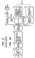
- Fig. 1 shows a recording head of the present invention.
- the recording element described above is denoted by reference numeral 11.
- a rear-surface electrode and a wiring pattern on a substrate 19 are electrically connected by silver paste 10, and 55 bonding dies are formed in the ceramic substrate 19.
- This substrate 19 and a driving substrate 18 on which driving controllers 22 to 24 and the like are mounted are fixed to an aluminum substrate 17.
- wire bonding pads formed on the surface of the recording element 11 and driving signal lines on the driving substrate 18 are connected by wire bonding using bonding wires 15 which connect the bonding pads and the inner surfaces of through holes 16 connected to the driving signal lines at the end of the driving substrate 18.
- the inner surfaces of the through holes 16 are plated with gold about 0.5 ⁇ m thick by using a pattern 12. The through holes 16 are then cut in substantially the center to have a semicircular shape.
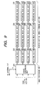
- Fig. 5B shows the state of the cut section.
- the inner surface of the through hole 16 connected by wire bonding shown in Fig. 1 is a semicircular surface shown in Fig. 5B.
- Fig. 6 shows the state in which the bonding pads on the recording element 11 are connected to the inner surfaces of the through holes 16 by the bonding wires 15. Note that a power supply for supplying power from the rear surface of the recording element 11 and the like component are not shown. Analogously, the through holes 16 of the driving substrate 18 are directly connected to the pattern on the ceramic substrate 19 by wire bonding.
- the driving controllers 22 to 24 described earlier are mounted on the substrate 18 as several driving ICs.
- the driving substrate 18 is placed on one side of the substrate 19 on which the recording element 11 is mounted.
- two driving substrates 18 can also be similarly arranged and connected on the two sides.
- a light-emitting element having a self-scanning function is used as the recording element, the present invention is naturally applicable to an LED, an LCD, or an EL using normal matrix driving.
- the two substrates are arranged close to each other so that the upper surface of the first substrate and the inner surfaces of the through holes formed in the second substrate are substantially flush with each other. In this state, the bonding pads of the recording element and the inner surfaces of the through holes are connected by the bonding wires.
- Fig. 7 is a schematic view showing the construction of a color copying machine using the recording head of the present invention.
- Figs. 8A and 8B are block diagrams showing the configuration of a digital image processing unit 612.
- Fig. 9 is a block diagram showing the arrangement of an LED image recording section.
- the recording head of the present invention constitutes a recording head drive section and a recording head section in the printer section to be described later.
- the color reader section is shown in the upper portion of Fig. 7.
- a CCD 401 is mounted on a substrate 611.
- An image processor 612 includes a unit 501 and sections 502 to 505 in Fig. 9 except for the CCD 401 in Fig. 7.
- An original glass plate (platen) 601 is arranged below a document feeder (DF) 602 (a mirror-surface press plate (not shown) can also be used instead of this document feeder 602).
- Light sources (halogen lamps or fluorescent lamps) 603 and 604 illuminate an original. Reflectors 605 and 606 direct the light from the light sources 603 and 604 onto an original.
- Mirrors 607 to 609 reflect the light, and a lens 610 focuses the reflected light from an original or the projected light onto the CCD 401.
- a carriage 614 carries the halogen lamps 603 and 604, the reflectors 605 and 606, and the mirror 607.
- a carriage 615 carries the mirrors 608 and 609.
- An interface (I/F) unit 613 interfaces with another IPU or the like.
- the carriages 614 and 615 mechanically move at velocities V and V/2, respectively, in a direction perpendicular to the electrical scan (main scan) direction of the CCD 401, thereby scanning (sub-scanning) the entire surface of an original.
- the color reader section also includes an operation unit 600 of the copying machine and a driving means 616 for the carriages 614 and 615.
- Figs. 8A and 8B are block diagrams showing a detailed configuration of the digital image processing unit 612.
- An original on the original glass plate reflects the light from the light sources 603 and 604.
- the reflected light is guided to the CCD 401 and converted into electrical signals (if the CCD 401 is a color sensor, RGB color filters can be arranged in-line in the order of R, G, and B on a one-line CCD or an R filter, a G filter, and a B filter can be arranged on three-line CCDs, and these filters can be formed on a chip or separated from a CCD).
- the electrical signals (analog image signals) are applied to the image processing unit 612 and sampled-and-held (S/H) by a clamp & amp.
- the dark levels of the analog image signals are clamped to a reference potential, and the signals are amplified to a predetermined level (the processing order is not restricted to the one described above) and A/D-converted into, e.g., R, G, and B digital signals each having 8 bits.
- the R, G, and B signals are subjected to shading correction and black correction in a shading section 403 and transferred to a concatenation & MTF correction & original detection section 404. If the CCD 401 is a three-line CCD, the reading position differs from one line to another.
- concatenation is so performed as to adjust the delay amount of each line in accordance with the reading speed, thereby correcting the signal timings such that the three lines are read in the same position. Since the reading MTF changes in accordance with the reading speed or the magnification, MTF correction is so performed as to correct this change. Also, the original size is detected by original detection by scanning the original on the original glass plate. The digital signals whose reading position timings are thus corrected are applied to an input masking section 405 where the spectral characteristics of the CCD 401 and the spectral characteristics of the light sources 603 and 604 and the reflectors 605 and 606 are corrected.
- the output from the input masking section 405 is applied to a selector 406 capable of selecting an external I/F signal from an external I/F unit 414 in the I/F unit 613.
- the output signal from the selector 406 is applied to a color space compression & grounding elimination & log conversion section 407 and a grounding removing section 415.
- the signal is applied to a black letter discriminating section 416 for discriminating black letters from the original.
- the black letter discriminating section 416 generates a black letter signal from the original.
- color space compression is so performed as to check whether the read image signal falls in a range within which the signal can be reproduced by a printer. If the image signal falls in this range, no correction is performed. If the image signal falls outside the range, the image signal is so corrected as to fall within the range in which the signal can be reproduced by the printer. Grounding elimination processing is then performed, and the resulting R, G, and B signals are LOG-converted into C, M, and Y signals.
- the timing of the output signal from the color space compression & grounding elimination & log conversion section 407 is adjusted by a delaying section 408 so as to match the timing of the signal generated by the black letter discriminating section 416.
- Moiré is removed from these two types of signals by a moiré eliminating section 409, and the signals are subjected to variable power processing in the main scan direction by a variable power processing section 410.
- UCR processing is performed for the C, M, and Y signals processed by the variable power processing section 410 to generate C, M, Y, and K signals, which are corrected into signals matching the printer output by masking processing.
- the discrimination signal generated by the black letter discriminating section 416 is fed back to the C, M, Y, and K signals.
- the density of the signal processed by the UCR & masking & black letter reflection section 411 is adjusted by a ⁇ correction section 412.
- the signal is then subjected to smoothing or edge processing by a filter section 413.
- the processed signal is converted from an 8-bit multivalue signal into a binary signal by a binary conversion unit 501 shown in Fig. 9. (The conversion method can be any of the dither method, error diffusion method, and improved error diffusion method.)
- the printer section is shown in the lower portion of Fig. 7.
- This printer section includes an M image forming unit 617, a C image forming unit 618, a Y image forming unit 619, and a K image forming unit 620. Since these image forming units have the same construction, the M image forming unit 617 will be described in detail below, and a description of the other image forming units will be omitted.
- the recording heads of the present invention form recording head drive sections 506 to 509 and recording head sections 510 to 513 shown in Fig. 9.
- a latent image is formed on the surface of a photosensitive drum 642 by light from the recording head section 510.
- a primary charger 621 charges the surface of the photosensitive drum 642 to a predetermined potential, thereby preparing for latent image formation.
- a developing device 622 develops the latent image on the photosensitive drum 642 to form a toner image.
- the developing device 622 includes a sleeve 645 for performing development by applying a developing bias.
- a transfer charger 623 performs discharge from the back surface of a transfer belt 633, thereby transferring the toner image on the photosensitive drum 642 onto a recording sheet or the like on the transfer belt 633.
- no cleaning unit is included in the apparatus because the transfer efficiency is high (it is of course possible to use a cleaning unit with no problem).
- Recording sheets or the like stored in cassettes 640 and 641 are picked up one by one by pickup rollers 639 and 638 and supplied onto the transfer belt 633 by paper feed rollers 636 and 637.
- a supplied recording sheet is charged by a chuck charger 646.
- a transfer belt roller 648 drives the transfer belt 633 and charges the recording sheet in combination with the chuck charger 646, thereby chucking the recording sheet to the transfer belt 633.
- a sheet leading end sensor 647 senses the leading end of the recording sheet on the transfer belt 633.
- a detection signal from the sheet leading end sensor is supplied from the printer section to the color reader section and used as a sub-scan sync signal when the color reader printer sends a video signal to the printer section.
- the recording sheet is conveyed by the transfer belt 633, and toner images are formed on the recording sheet in the order of M, C, Y, and K by the image forming units 617 to 620.
- the recording sheet passing through the K image forming unit 620 is charge-removed by a charge remover 649 to facilitate separation from the transfer belt 633 and separated from the transfer belt 633.
- a separation charger 650 prevents image disturbance caused by separation discharge when the recording sheet is separated from the transfer belt 633.
- the separated recording sheet is charged by pre-fixing chargers 651 and 652.
- the toner image is thermally fixed by a fixing device 634, and the recording sheet is delivered to a sheet delivery tray 635.
- the binary CMYK image signal generated by the image processing unit shown in Figs. 8A and 8B and supplied to the binary conversion unit 501 is then applied to the delaying sections 502 to 505 where the differences between the distances from the sheet leading end sensor 647 and the image forming units 617 to 620 are adjusted on the basis of the sheet leading end signal from the sheet leading end sensor 647. This allows the four colors to be printed in predetermined positions.
- the recording head drive sections 506 to 509 generate signals for driving the recording head sections 510 to 513.
- the light-emitting elements (recording head sections) arranged in line emit or do not emit light in accordance with the recording signal (image signal), thereby recording on the photosensitive drum.
- the recording head of the present invention is small in size. Therefore, a small-diameter photosensitive drum can be used in an image forming apparatus using this recording head. This enables miniaturization of the image forming apparatus itself.
Description
Claims (9)
- A recording head comprising:a recording element (11) having a plurality of light-emitting elements, said recording element having a bonding pad;a first substrate (19) on which said recording element (11) is mounted;a driving unit (22) for driving said recording element;a second substrate (18) on which said driving unit is mounted, said second substrate having a through hole (16) intersecting an edge;
anda bonding wire (15) for connecting said bonding pad and an inner surface of said through hole (16). - A head according to claim 1, wherein said recording element (11) has a self-scanning function.
- A head according to claim 1 or claim 2, wherein said first and second substrates (19) and (18) are arranged close to each other so that an upper surface of said first substrate (19) and the inner surface of said through hole (16) are substantially flush with each other.
- An image forming apparatus comprising:a recording element (11) having a plurality of light-emitting elements, said recording element having a bonding pad;a first substrate (19) on which said recording element (11) is mounted;a driving unit (22) for driving said recording element;a second substrate (18) on which said driving unit is mounted, said second substrate (18) having a through hole (16) intersecting an edge;a bonding wire (15) for connecting said bonding pad and an inner surface of said through hole (16); anda photosensitive medium (642) on which said recording element (11) records.
- An apparatus according to claim 4, wherein said recording element (11) has a self-scanning function.
- An apparatus according to claim 4 or claim 5, wherein said first and second substrates (19, 18) are arranged close to each other so that an upper surface of said first substrate (19) and the inner surface of said through hole (16) are substantially flush with each other.
- A method of manufacturing a recording head, comprising the steps of:mounting a recording element (11) having a plurality of light-emitting elements and a bonding pad on a first substrate (19);forming a through hole (16) in a second substrate (18);forming an edge of the second substrate intersecting said through hole;mounting a driving unit (22) for driving said recording element (11) on said second substrate (18); andconnecting said bonding pad and an inner surface of said through hole (16) by a bonding wire (15).
- A method according to claim 7, further comprising the step of arranging said first and second substrates (19) and (18) close to each other so that an upper surface of said first substrate (19) and the inner surface of said through hole (16) are substantially flush with each other.
- A method according to claim 7 or claim 8, wherein said recording element (16) has a self-scanning function.
Applications Claiming Priority (3)
| Application Number | Priority Date | Filing Date | Title |
|---|---|---|---|
| JP16474/97 | 1997-01-30 | ||
| JP1647497 | 1997-01-30 | ||
| JP1647497A JPH10211732A (en) | 1997-01-30 | 1997-01-30 | Head and method for mounting the same |
Publications (2)
| Publication Number | Publication Date |
|---|---|
| EP0856411A1 EP0856411A1 (en) | 1998-08-05 |
| EP0856411B1 true EP0856411B1 (en) | 2003-01-08 |
Family
ID=11917281
Family Applications (1)
| Application Number | Title | Priority Date | Filing Date |
|---|---|---|---|
| EP98101080A Expired - Lifetime EP0856411B1 (en) | 1997-01-30 | 1998-01-22 | Recording head and image forming apparatus using the same |
Country Status (4)
| Country | Link |
|---|---|
| US (1) | US6025858A (en) |
| EP (1) | EP0856411B1 (en) |
| JP (1) | JPH10211732A (en) |
| DE (1) | DE69810520T2 (en) |
Families Citing this family (16)
| Publication number | Priority date | Publication date | Assignee | Title |
|---|---|---|---|---|
| JPH11216896A (en) * | 1998-02-03 | 1999-08-10 | Fujitsu Ltd | Exposure apparatus |
| JP4066501B2 (en) * | 1998-04-10 | 2008-03-26 | 富士ゼロックス株式会社 | Two-dimensional light emitting element array and driving method thereof |
| JP2000094745A (en) * | 1998-09-25 | 2000-04-04 | Fuji Xerox Co Ltd | Image-forming apparatus and two-dimensional light- emitting element array |
| JP2000203078A (en) * | 1999-01-18 | 2000-07-25 | Canon Inc | Drive controller and control method |
| US6563526B1 (en) * | 1999-01-22 | 2003-05-13 | Canon Kabushiki Kaisha | Image formation apparatus |
| JP3428929B2 (en) * | 1999-07-30 | 2003-07-22 | キヤノン株式会社 | LED array device and image forming device |
| JP2001096802A (en) * | 1999-10-04 | 2001-04-10 | Canon Inc | Method for production of led array head |
| JP4511016B2 (en) * | 2000-11-29 | 2010-07-28 | 京セラ株式会社 | Optical printer head |
| US6896796B2 (en) * | 2001-02-16 | 2005-05-24 | W. R. Grace & Co.-Conn. | Membrane separation for sulfur reduction |
| JP2005175417A (en) * | 2003-07-28 | 2005-06-30 | Ricoh Co Ltd | Light emitting element array, light writing unit, and image forming apparatus |
| US7151557B2 (en) * | 2004-03-19 | 2006-12-19 | Lexmark International, Inc. | Collimation assembly for adjusting laser light sources in a multi-beamed laser scanning unit |
| WO2007097347A1 (en) * | 2006-02-20 | 2007-08-30 | Kyocera Corporation | Light emitting element array, light emitting device, and image forming device |
| JP4837611B2 (en) * | 2007-03-30 | 2011-12-14 | 株式会社沖データ | Semiconductor device and print head |
| JP4656227B2 (en) * | 2008-11-11 | 2011-03-23 | 富士ゼロックス株式会社 | Light emitting element head and image forming apparatus |
| JP6543579B2 (en) * | 2016-01-28 | 2019-07-10 | 株式会社沖データ | Optical head, image forming apparatus, and image reading apparatus |
| JP6550342B2 (en) * | 2016-01-29 | 2019-07-24 | 株式会社沖データ | Light emitting element unit, exposure apparatus, image forming apparatus, and method of manufacturing light emitting element unit |
Family Cites Families (8)
| Publication number | Priority date | Publication date | Assignee | Title |
|---|---|---|---|---|
| CA1023039A (en) * | 1975-02-28 | 1977-12-20 | Bowmar Canada Limited | Light emitting diode display |
| US4843280A (en) * | 1988-01-15 | 1989-06-27 | Siemens Corporate Research & Support, Inc. | A modular surface mount component for an electrical device or led's |
| JP2577034B2 (en) * | 1988-03-18 | 1997-01-29 | 日本板硝子株式会社 | Self-scanning light emitting element array and driving method thereof |
| DE68929071T2 (en) * | 1988-03-18 | 2000-02-03 | Nippon Sheet Glass Co Ltd | Self-scanning arrangement of light-emitting components |
| JP2784025B2 (en) * | 1989-02-07 | 1998-08-06 | 日本板硝子株式会社 | Optical scanning device |
| JPH02292064A (en) * | 1989-04-28 | 1990-12-03 | Nec Niigata Ltd | Led printing head |
| DE4308896C2 (en) * | 1993-03-19 | 1994-12-22 | Siemens Nixdorf Inf Syst | Print head for an electrographic printing device |
| JPH07228003A (en) * | 1993-12-22 | 1995-08-29 | Kyocera Corp | Image apparatus |
-
1997
- 1997-01-30 JP JP1647497A patent/JPH10211732A/en active Pending
-
1998
- 1998-01-22 EP EP98101080A patent/EP0856411B1/en not_active Expired - Lifetime
- 1998-01-22 DE DE69810520T patent/DE69810520T2/en not_active Expired - Lifetime
- 1998-01-22 US US09/010,790 patent/US6025858A/en not_active Expired - Lifetime
Also Published As
| Publication number | Publication date |
|---|---|
| EP0856411A1 (en) | 1998-08-05 |
| US6025858A (en) | 2000-02-15 |
| DE69810520T2 (en) | 2003-05-15 |
| DE69810520D1 (en) | 2003-02-13 |
| JPH10211732A (en) | 1998-08-11 |
Similar Documents
| Publication | Publication Date | Title |
|---|---|---|
| EP0856411B1 (en) | Recording head and image forming apparatus using the same | |
| US7847978B2 (en) | Image reading apparatus and image reading method | |
| US4706130A (en) | Image recording apparatus utilizing light emitting diodes with pixel shape correction | |
| US5233442A (en) | Photosensor and image reading device with improved correction means for signal correction and image reading method | |
| US6008833A (en) | Light-emitting device and image forming apparatus using the same | |
| US5272548A (en) | Photosensor and image reading device with improved correction means for signal correction and image reading method | |
| US5969744A (en) | Recording head and image forming apparatus using the same | |
| US6195183B1 (en) | Image reading apparatus and image sensor chip thererfor | |
| US20060291006A1 (en) | Image sensor and image reading apparatus | |
| US6295077B1 (en) | Image forming apparatus | |
| US6804033B1 (en) | Image processing apparatus and method, and image processing system | |
| US6069644A (en) | Recording head and image forming apparatus using the same | |
| US7224483B2 (en) | Image signal correction light source that can cope with dust and scratch on transparent document, and its control | |
| US7064872B1 (en) | Exposure control for a CCD scanner | |
| JP4065515B2 (en) | Image reading device | |
| EP0791471B1 (en) | Recording head and image forming apparatus using the same | |
| US6489601B1 (en) | Correction method for an image reading system | |
| JP2003115584A (en) | Imaging apparatus and reader | |
| KR100408265B1 (en) | Color image scanner | |
| US11647142B2 (en) | Image reading apparatus | |
| JP2000006466A (en) | Led power source apparatus and led power controlling method | |
| JP2005070463A (en) | Image reader | |
| JPH11129534A (en) | Image recording apparatus | |
| JP2003084536A (en) | Image forming apparatus | |
| JPH1175037A (en) | Image forming device and computer readable storage medium |
Legal Events
| Date | Code | Title | Description |
|---|---|---|---|
| PUAI | Public reference made under article 153(3) epc to a published international application that has entered the european phase |
Free format text: ORIGINAL CODE: 0009012 |
|
| AK | Designated contracting states |
Kind code of ref document: A1 Designated state(s): DE FR GB |
|
| AX | Request for extension of the european patent |
Free format text: AL;LT;LV;MK;RO;SI |
|
| 17P | Request for examination filed |
Effective date: 19990204 |
|
| AKX | Designation fees paid |
Free format text: DE FR GB |
|
| RBV | Designated contracting states (corrected) |
Designated state(s): DE FR GB |
|
| 17Q | First examination report despatched |
Effective date: 20010131 |
|
| GRAG | Despatch of communication of intention to grant |
Free format text: ORIGINAL CODE: EPIDOS AGRA |
|
| GRAG | Despatch of communication of intention to grant |
Free format text: ORIGINAL CODE: EPIDOS AGRA |
|
| GRAH | Despatch of communication of intention to grant a patent |
Free format text: ORIGINAL CODE: EPIDOS IGRA |
|
| GRAH | Despatch of communication of intention to grant a patent |
Free format text: ORIGINAL CODE: EPIDOS IGRA |
|
| GRAA | (expected) grant |
Free format text: ORIGINAL CODE: 0009210 |
|
| AK | Designated contracting states |
Kind code of ref document: B1 Designated state(s): DE FR GB |
|
| REG | Reference to a national code |
Ref country code: GB Ref legal event code: FG4D |
|
| REF | Corresponds to: |
Ref document number: 69810520 Country of ref document: DE Date of ref document: 20030213 Kind code of ref document: P |
|
| ET | Fr: translation filed | ||
| PLBE | No opposition filed within time limit |
Free format text: ORIGINAL CODE: 0009261 |
|
| STAA | Information on the status of an ep patent application or granted ep patent |
Free format text: STATUS: NO OPPOSITION FILED WITHIN TIME LIMIT |
|
| 26N | No opposition filed |
Effective date: 20031009 |
|
| REG | Reference to a national code |
Ref country code: FR Ref legal event code: PLFP Year of fee payment: 19 |
|
| REG | Reference to a national code |
Ref country code: FR Ref legal event code: PLFP Year of fee payment: 20 |
|
| PGFP | Annual fee paid to national office [announced via postgrant information from national office to epo] |
Ref country code: FR Payment date: 20161215 Year of fee payment: 20 |
|
| PGFP | Annual fee paid to national office [announced via postgrant information from national office to epo] |
Ref country code: DE Payment date: 20170117 Year of fee payment: 20 |
|
| PGFP | Annual fee paid to national office [announced via postgrant information from national office to epo] |
Ref country code: GB Payment date: 20170118 Year of fee payment: 20 |
|
| REG | Reference to a national code |
Ref country code: DE Ref legal event code: R071 Ref document number: 69810520 Country of ref document: DE |
|
| REG | Reference to a national code |
Ref country code: GB Ref legal event code: PE20 Expiry date: 20180121 |
|
| PG25 | Lapsed in a contracting state [announced via postgrant information from national office to epo] |
Ref country code: GB Free format text: LAPSE BECAUSE OF EXPIRATION OF PROTECTION Effective date: 20180121 |