EP0852813B1 - Integrated circuit device with embedded flash memory and method for manufacturing same - Google Patents
Integrated circuit device with embedded flash memory and method for manufacturing same Download PDFInfo
- Publication number
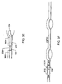
- EP0852813B1 EP0852813B1 EP97931196A EP97931196A EP0852813B1 EP 0852813 B1 EP0852813 B1 EP 0852813B1 EP 97931196 A EP97931196 A EP 97931196A EP 97931196 A EP97931196 A EP 97931196A EP 0852813 B1 EP0852813 B1 EP 0852813B1
- Authority
- EP
- European Patent Office
- Prior art keywords
- gate
- floating gate
- oxide
- dielectric
- floating
- Prior art date
- Legal status (The legal status is an assumption and is not a legal conclusion. Google has not performed a legal analysis and makes no representation as to the accuracy of the status listed.)
- Expired - Lifetime
Links
Images




















Classifications
-
- H—ELECTRICITY
- H10—SEMICONDUCTOR DEVICES; ELECTRIC SOLID-STATE DEVICES NOT OTHERWISE PROVIDED FOR
- H10B—ELECTRONIC MEMORY DEVICES
- H10B41/00—Electrically erasable-and-programmable ROM [EEPROM] devices comprising floating gates
- H10B41/40—Electrically erasable-and-programmable ROM [EEPROM] devices comprising floating gates characterised by the peripheral circuit region
-
- H—ELECTRICITY
- H10—SEMICONDUCTOR DEVICES; ELECTRIC SOLID-STATE DEVICES NOT OTHERWISE PROVIDED FOR
- H10B—ELECTRONIC MEMORY DEVICES
- H10B41/00—Electrically erasable-and-programmable ROM [EEPROM] devices comprising floating gates
- H10B41/40—Electrically erasable-and-programmable ROM [EEPROM] devices comprising floating gates characterised by the peripheral circuit region
- H10B41/42—Simultaneous manufacture of periphery and memory cells
- H10B41/49—Simultaneous manufacture of periphery and memory cells comprising different types of peripheral transistor
-
- H—ELECTRICITY
- H10—SEMICONDUCTOR DEVICES; ELECTRIC SOLID-STATE DEVICES NOT OTHERWISE PROVIDED FOR
- H10D—INORGANIC ELECTRIC SEMICONDUCTOR DEVICES
- H10D30/00—Field-effect transistors [FET]
- H10D30/60—Insulated-gate field-effect transistors [IGFET]
- H10D30/68—Floating-gate IGFETs
- H10D30/6891—Floating-gate IGFETs characterised by the shapes, relative sizes or dispositions of the floating gate electrode
- H10D30/6892—Floating-gate IGFETs characterised by the shapes, relative sizes or dispositions of the floating gate electrode having at least one additional gate other than the floating gate and the control gate, e.g. program gate, erase gate or select gate
Definitions
- This invention relates generally to the field of integrated circuit devices, and more particularly relates to an integrated circuit device having embedded flash memory therein and to a method of manufacturing such a device.
- Non-volatile memory devices are an important and growing segment of the electronics industry. Non-volatile memory devices retain data or program information without the sustained application of power to the device. Electrically reprogrammable non-volatile memory devices allow the user to change the contents of the memory and retain that information after power is removed from the device: examples are electrically-erasable programmable read-only memory (EEPROM), and flash memory. Flash memory circuits enjoy lower costs than EEPROM since the number of transistors required to execute the memory function is reduced by a configuration which erases large (more than one bit) blocks of the memory in parallel or in a "flash.”
- EEPROM electrically-erasable programmable read-only memory
- Flash memory is a very rapidly growing segment of the microelectronics industry with applications in almost all types of electronic products and systems. For mass memory applications the cost of the memory function is very important. Increasingly, flash memory is employed in what has been termed "embedded" applications where the nonvolatile memory function is incorporated into some other kind of chip, such as a microcontroller, digital signal processor (DSP), disc drive controller, or the like. This embedded approach can improve overall system performance, reduce size and costs by eliminating the need for two separate chips.
- DSP digital signal processor
- Flash memory devices have increased value added in these embedded or highly integrated applications.
- traditional flash memory devices and manufacturing methods present challenges for embedded applications.
- Typical flash memory cells switch information more slowly than similar CMOS ROM cells. This means that either flash memory must be supplemented by faster-switching volatile memory or the system performance must be slowed to the point where flash memory can keep up.
- many flash memory devices require greater than 30% increases in manufacturing steps when compared to typical CMOS devices.
- a flash memory device which offers high performance in switching speed with rates close to that of standard CMOS would be of great benefit to embedded applications.
- Two significant embedded applications where flash memory speed directly affects throughput or chip speed are DSP and microcontrollers. Further devices are known from WO 94/10706 , US 5455792 .
- the present invention as claimed in claim1 relates to a electrically-alterable non-volatile information storage device with applications in data, program storage and the manufacture of programmable logic.
- the disclosed devices are well-suited to "flash" memory applications in which data is written for storage as bits, bytes, or pages but which is generally erased for rewriting in larger blocks of memory.
- the disclosed memory device allows the use of flash memory in higher-speed applications enabling new types of useful electronic circuits and systems.
- the invention consists of a higher performance cell with merged floating gate and control gate.
- the higher performance capability of this flash cell device is achieved at low cost by the disclosed cell's unique architecture by using the disclosed methods.
- the cell design and manufacturing methods allow the use of thin dielectrics to gate the conduction channel of the device, thus enabling higher on current performance.
- the memory device in accordance with the present invention functions in all current applications for flash memory and is cost competitive in manufacture. However, the memory device in accordance with the present invention offers significant improvements in performance over competing technologies.
- the excellent switching properties, low off current and high on current of a device in accordance with the present invention also allows it to be employed to replace EEPROM, fuses, anti-fuses or other electrically-alterable non-volatile switching devices in programmable logic devices.
- the memory device in accordance with the present invention can be fabricated with low cost methods. Numerous practical low cost alternative manufacturing flows are disclosed herein to build the new memory device. Unique cell layout and process sequences are defined for each basic method. A method to make self aligned cuts in polysilicon is used in one of the alternative methods of manufacture not forming part of the claimed invention. The manufacturing methods in accordance with the present invention are compatible with current tools and procedures, allowing the memory device in accordance with the invention to be added to CMOS circuits to replace masked ROM with more flexible Flash memory at a modest increase in cost.
- the cell operational method and manufacturing methods in accordance with the present invention allow the size of this memory element to be scaled smaller to maintain a low cost and high performance as the minimum feature size of microelectronic circuits is reduced in the future.
- the disclosed cell approach also offers simpler programming methods to simplify memory array design, supports higher cell currents for high speed applications and uses lower cost manufacturing methods than the more common "ETOX" cell approach.
- a new etching technique is disclosed which can used in the manufacture of the disclosed cell which allows a very thin gap to be etched in a polysilicon layer.
- novel process methods are disclosed that enable the cell to be manufactured in a practical manner by allowing thin dielectrics layers which are formed early in the process to be protected while dielectric is removed in other locations.
- the memory device in accordance with the present invention can be used for both embedded and stand-alone applications.
- the inherent switching speed of a device in accordance with the present invention can be about 200% (or more) faster than typical flash memory devices.
- the manufacture of this device is compatible with conventional CMOS process technologies and requires only about 25% increase in the number of manufacturing steps to add flash memory devices to a CMOS process.
- the high performance and modest cost of a memory device in accordance with the present invention allows it to be used in many high and low performance applications.
- Applications of the present invention can range from high-speed non volatile memory embedded within another type of integrated circuit, to high performance non-volatile switches in programmable logic devices.
- a cell in accordance with the present invention could also be used competitively for low speed mass memory applications.
- the disclosed high performance Flash memory cell teaches a novel way to manufacture a split gate Flash memory cell in which each device contains a word line gate and a floating gate which sets the state of the cell.
- An erase control gate is provided to control potentials associated with program and erasure of the cells. High potentials required for programming and erase operations are applied to the erase control gate and do not directly appear across the word line gate or the floating gate.
- This feature allows the dielectrics employed for the word line gate to be thinner, since the word line gate will not need to withstand the higher programming and erase biases. The result is a higher on state current and a dense cell geometry.
- the practical realization of the memory cell requires the use of new process methods and unique process sequences which are described in the four embodiments of the invention described below.
- the method preferred for a given manufacturing plant will be influenced by available tooling and experience with specific methods needed for the realization of the three gate cell. Also, certain embodiments have certain performance advantages or may be more easily optimized to achieve desired results. Moreover, certain embodiments can be made more densely than other embodiments. Thus, which embodiment is preferred will depend on manufacturing, performance, and design constraints as noted herein. Furthermore, the desired or available power supply voltages and other desired electrical specifications for the cell may suggest that one embodiment will be more desirable than another.
- CMOS Complementary-Metal-Oxide-Semiconductor
- the CMOS circuitry generally consists of all of the other circuitry used on the flash memory device that does not constitute the anay of cells, and performs circuit functions necessary to routing signals to and form the array, such as decoding.
- the low voltage CMOS transistors are used to perform logical functions are designed to handle nominal voltages signal (e.g., 5 Volts), while the high voltage CMOS transistors are used to shuttle higher voltage signals (e.g., 12 Volts) to the array to perform the erasing and programming functions. Because of the application of higher voltages to the high voltage CMOS transistors, these devices will typically require a thicker gate oxide thickness underneath their gates to prevent oxide wear out or breakdown. Also, the high voltage CMOS junctions will normally need to be deeper and more smoothly graded to sustain high voltages without going into avalanche breakdown.
- the layer thicknesses in the figures are not perfectly drawn to scale. The reader should consult the discussion accompanying the relevant figure in order to determine a layer's actual target thickness.
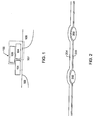
- FIG. 1 A comparative example of a memory cell is shown in FIG. 1 .
- the cell in FIG. 1 is comprised of two transistors in series, namely a word line gate transistor 101 and a storage transistor 102.
- Storage transistor 102 further consists of an erase control gate 103 and a floating gate 104. Diffused regions appear on the outside edges of the two transistors which constitute a bit line diffusion 105 and a source diffusion 106.
- the cell of FIG. 1 would typically be built on a lightly doped p-type crystalline substrate 107.
- the memory cell shown in FIG. 1 can be made by executing the following sequence of steps, which can be best appreciated with reference to the cross-sectional diagrams of Figs. 2 through 6 .
- field oxide regions 202 are thermally grown in a lightly p-doped silicon crystalline substrate 201 for the purpose of electrically isolating different cells from one another and isolating the cells from the CMOS transistors in the periphery.
- a high quality thermal oxide 203 is grown on the wafer surface to a thickness which depends upon the desired thickness of the gate oxide to be employed in the low voltage CMOS oxide transistor.
- a polysilicon layer 204 is deposited on top of the thermal oxide 203 to a preferred thickness of 2000 to 3000 Angstroms.
- polysilicon layer 204 has been etched to define the outer edges of word line gate 101 and floating gate 104.
- a gap 301 has been anisotropically etched to define the inner edges of word line gate 101 and floating gate 104. Both the gap and the outer edges may be simultaneously patterned and etched using traditional photolithography processing methods.
- This method supports effective hot electron programming of floating gate 104 by source side injection and also provides a much smaller layout than could be achieved with conventional methods.
- polysilicon 204 is covered with a nitride layer 3B01 to a preferred thickness of 2,000 to 4,000 Angstroms.
- the nitride layer is then patterned and etched by traditional means leaving the structure shown in FIG. 3B .
- FIG. 3C which shows a magnified view of the nitride window etched in FIG. 3B
- the exposed polysilicon 204 is oxidized, forming an oxide layer 3C01 which is preferably 100 to 200 Angstroms thick. Notice that nitride layer 3B01 is not subject to oxidation.
- FIG. 3C which shows a magnified view of the nitride window etched in FIG. 3B .
- nitride 3B01 is subject to an isotropic etch to remove a very small amount of nitride 3B01 on all edges of nitride 3B01.
- the etchant used to remove the nitride should not substantially attack the polysilicon 204 or oxide 3C01, and a solution of dilute hot phosphoric acid is suggested.
- the polysilicon 204 is anisotropically etched where exposed. Where the polysilicon 204 is protected by either nitride 3B01 or oxide 3C01, it will remain intact. Where the polysilicon is etched away, it forms gap 301 seen in FIG. 3A .
- oxide 3C01 constitutes the floating gate 104.
- the remaining nitride 3B01 is then removed after etching the gap 301.
- a photoresist 3F01 is applied over the polysilicon 204 and pattern, leaving the structure shown.
- the exposed polysilicon 204 is anisotropically etched, and the photoresist 3F01 is then removed, leaving the structure shown.
- the oxide 3C01 has not been removed and will act to protect the underlying polysilicon 204 from the anisotropic etch. Notice that this etch defines the outside edge of the word line 101 as well as the low voltage CMOS transistor gate 302.
- Oxide 203 acts as the gate oxide for the floating gate 104, the word line gate 101, and the low voltage CMOS gate 302.
- This etching technique used to form gap 301 allows for the formation of an extremely thin gap in polysilicon 204.
- the gap's thickness can be tightly controlled by controlling the etch rate of the overlying nitride 3C01.
- This technique has utility above that simply disclosed in formation of the above Flash EPROM cell. Because the gap that is produced is very thin, it can be used to form a series of transistor gates which do not require significant layout area for a diffusion or other connection between the gates to help jumper a signal through the gate series. A lower series resistance can be achieved by implanting dopants into the gap after the etch. However, in applications where a slightly higher resistance can be tolerated, no special implant or method is needed to allow the channel of the storage gate 102 to communicate with the word line gate 101.
- FIG. 3H a top down view is shown of the cross sectional structure shown in Fig 3A , which is marked by vantage point 3H01. Notice that the floating gate 104 has been etched on four sides by the photolithography step discussed in FIG. 3A .
- the wafer is next subjected to oxidation to increase the thickness of the oxide on the exposed silicon surfaces to from the dielectrics for the high voltage transistors.
- the total oxide thickness should be about 250 to 400 Angstroms for best results.
- oxide 401 appears over the floating gate it is referred to as interpoly oxide 402.
- Oxide 401 should be grown to a thickness which will perform optimally when used as both an interpoly oxide and as the gate oxide for the high voltage CMOS transistors. A thickness of approximately 300 Angstroms is preferred.
- a second layer of polysilicon 403 is deposited on the surface of the wafer.
- polysilicon layer 403 is patterned and anisotropically etched using traditional photolithography methods. This etch defines erase control gate 103. Notice that high voltage CMOS transistor gate 501 is also defined by the etching of polysilicon layer 403 and that oxide 401 provides the gate oxide for the high voltage CMOS transistor. Polysilicon layer 403 should be patterned to produce an erase control gate 103 which overlaps with the underlying floating gate 104 in order to optimize coupling between these two gates.
- low voltage diffusions 601 and high voltage diffusions 602. This is accomplished by first masking off the low voltage diffusion regions and performing an ion implantation step.
- the ion implantation step causes ions to bombard perpendicularly into the wafer surface. Where the ions become embedded into substrate 201 a high voltage diffusion 601 will be formed.
- the ions will be of a character (e.g., phosphorous or arsenic) to impart an n-type character to the substrate 201 in the high voltage diffusions 601. Because the low voltage regions are masked off, no ions will be implanted into the substrate 201 in those regions.
- high voltage diffusion regions 602 are then masked into order to ion implant the low voltage diffusions 601 in the same manner as previously described. Notice that the ion implantation process and subsequent appropriate thermal drive of the ions are engineered such that the high voltage diffusions 602 are deeper and more smoothly graded than the low voltage diffusions 601 and can therefore carry a higher voltage signal without breaking down. Where the low voltage diffusion appears adjacent to word line gate 101 it is referred to as bit line diffusion 105. Where the high voltage diffusion appears adjacent to floating gate 104 it is referred to as source diffusion 106.
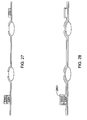
- FIG. 7 shows a top down view of two cells after performing the processes described with reference to Figs. 2 through 6 .
- each cell's source diffusion 106 is common to all other cells' source diffusion and each cell's bit line diffusion 105 is shared with only one other cell's bit line diffusion.
- the vantage point shown in FIG. 1 is denoted by 701.
- Among the advantages of this first embodiment are higher density and lower costs due to the processing sequence that allows the self aligned formation of a floating gate and word line gate from the same layer of polysilicon. This lowers manufacturing costs, increases layout density, and allows greater flexibility in the selection of erase control gate to floating gate coupling ratio.
- the thin gate oxides are formed first, and the interpoly oxide is formed with the floating gate and low voltage CMOS gates already defined. No additional processing steps are required to insure isolation between the floating gate and the word line gate.
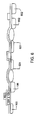
- FIG. 8 A first embodiment of a memory cell in accordance with the present invention is shown in FIG. 8 .
- the cell in Fig. 8 is comprised, as in the first embodiment, of two transistors in series, namely a word line gate transistor 801 and a storage transistor 802.
- Storage transistor 802 further consists of an erase control gate 803 and a floating gate 804. Diffused regions appear on the outside edges of the two transistors which con-mtute bit line diffusion 805 and source diffusion 806.
- the memory cell shown in FIG. 8 can be made by executing the sequence of steps to be described with reference to Figs. 9 through 20 .
- field oxide regions 902 are thermally grown in a lightly p-doped silicon crystalline substrate 901.
- field isolation methods such as shallow trench and refill may also be applied in lieu of lower cost local oxidation of silicon method.
- a high quality thermal oxide 903 is grown on the wafer surface to a thickness of 100 Angstroms in a presently preferred embodiment.
- a polysilicon layer 904 is deposited on top of thermal oxide 903 to a thickness of approximately 500 Angstroms in a presently preferred embodiment.
- polysilicon layer 904 has been patterned and etched using traditional photolithography methods. Notice that polysilicon layer 904 has been left only in the array and will be used to form the floating gate 804.
- FIG. 10B a top view is shown of the cross sectional structure shown in Fig 10A , which is marked by vantage point 10B01. Notice that polysilicon layer 904 has had slots etched into it where it lies over oxide 902 in the array by the photolithography step described with reference to FIG. 10A .
- a high quality interpoly oxide 1101 is formed.
- the preferred method is a combination of thermal oxidation followed by the deposition of oxide by Chemical Vapor Deposition (CVD). It is complicated to predict what method would be best. CVD oxide for part of the oxidation gives better control over the shape of the interpoly oxide and can reduce cell disturb problems. When polysilicon over field oxide is oxidized an inverse point can form which tends to cause field enhancement. Oxide 1101 can also be formed by only thermal oxidation which would in turn leave only about 250 Angstroms on the exposed portions of substrate 901 because doped polysilicon will oxidize faster than the lightly doped crystalline silicon.
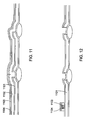
- a second layer of polysilicon 1102 is deposited on the surface of the wafer to preferred thickness of 2000 Angstroms.
- an oxide layer 1103 is formed on top of polysilicon 1102 to a preferred thickness of 400 Angstroms.
- silicon nitride (nitride) 1104 is deposited on top of oxide 1103 to a preferred thickness of 500 to 1000 Angstroms.
- nitride 1104, oxide 1103, and polysilicon layer 1102 have been etched using traditional photolithography techniques to define the outer edges of erase control gate 803. Because each of these layers requires the use of different etchants, each layer is etched separately using dry etching.
- the spacer process preferably comprises depositing approximately 1000 to 2500 Angstroms of oxide or nitride over the structure in FIG. 12 , and subjecting the deposited oxide or nitride to an anisotropic dry etch which occurs perpendicular to the substrate 901. This etch will preferentially etch away the oxide overlying horizontal surfaces while leaving a spacer oxide 1301 covering the vertical surfaces.
- the spacer oxide 1301 will remain and will be about 75% as thick on the side of the erase control gate 803 as the original oxide or nitride film (e.g., 1000 to 2500 Angstroms in a preferred embodiment). Notice that the anisotropic etch is also used to remove interpoly oxide 1101 from the top of polysilicon 904. While the spacer oxide will also form on the vertical edges of the structures over field oxide 902, spacers in this location are unimportant and have not been drawn in FIG. 13 .
- the exposed portions of polysilicon 904 can be anisotropically etched using the overlying erase control gate 803 and spacer oxide 1301 as a mask. This etching step defines the outer edges of floating gate 804, thus self aligning floating gate 804 underneath the erase control gate 803. It is desirable to dry etch the polysilicon such that nitride 1104 is not substantially thinned to protect oxide 1103 from being attacked during subsequent cleaning steps. Retaining a maximum amount of oxide 1103 is desirable to minimize coupling between erase control gate 803 and word line gate 801 which has yet to be formed. However, this is not required to successfully manufacture this cell and the nitride may instead be completely removed at this point. Note also that the remaining nitride must ultimately be removed prior to salacide formation or contact formation to be formed much later in the process flow.
- the remaining nitride 1104, oxide 1103, and polysilicon 1102 in the high voltage CMOS area are patterned and etched using traditional photolithography methods. As described with reference to FIG. 12 , multi-step dry etching is used to remove these three materials individually. Notice that where polysilicon 1102 has been etched defines high voltage CMOS gates 1501. Notice also that interpoly oxide 1101 provides the gate oxide for high voltage CMOS transistor 1501.
- edge sealing it is desired to protect the oxide 903 under the floating gate 804 from subsequent chemical processing which is described with reference to FIG. 17 .
- This is referred to as edge sealing.
- the cell is oxidized at this stage to form a thin layer of oxide 1601 on the sides of the floating gate 804 to a preferred thickness of 200 Angstroms. This oxide will grow to a lesser extent where oxides are already present and is shown in FIG. 16 only where it overlies a transistor structure. Because oxide layer 1601 will not be thick enough to adequately protect against subsequent chemical etching, it is desired to also put dielectric spacers 1602 on the sides of floating gate 804.
- the general processing steps to form spacers are well known in the art and are described with reference to FIG. 13 .
- Dielectric spacers 1602 are also beneficial in that they will ultimately provide more insulation between floating gate 804 and erase control gate 803 from word line gate 801 which has not yet been formed.
- the spacers can be made several different ways with different potential advantages and drawbacks. Nitride spacers, while the cheapest from a manufacturing standpoint, may suffer from the drawback that during use of the cell electrons may become trapped in the nitride spacer thus inadvertently hampering the ability of the device to form a channel. Therefore, if nitride spacers are used for dielectric spacer 1602, they should preferably be made a thinly as possible to leave 150 to 250 Angstroms of spacer on the side of the floating gate. Alternatively, an oxide spacer could be used.
- An acceptable oxide spacer can be achieved by oxidizing a pre-formed polysilicon spacer in a steam ambient.
- the thickness of the polysilicon spacer can be engineered such that it is completely oxidized when performing the subsequent high quality thermal oxidation process described with reference to FIG. 18 , which would be approximately 150 Angstroms thick on the side of floating gate 804 prior to oxidation.
- the polysilicon can first be partially oxidized prior to the clean up described with reference to FIG. 17 that proceeds the high quality thermal oxidation step. To implement this, approximately 300 Angstroms of polysilicon is left on the side of floating gate 804, which is then be partially oxidized leaving approximately 180 Angstroms of the polysilicon spacer unoxidized. During the subsequent clean up step, the oxidized portion of the spacer is removed, leaving the 180 Angstroms or so of unoxidized polysilicon spacer. This remaining portion of the polysilicon spacer is subsequently oxidized during the high quality oxidation process described with reference to FIG. 18 .
- oxidized polysilicon spacers may be more expensive from a manufacturing standpoint, it is the presently preferred method because it can be expected to be superior in performance to nitride spacers; inadvertent trapping is minimized, while subsequent oxidation processes may be tailored independent of the edge sealing process described here.
- the dielectric spacers have been drawn in FIG. 16 such that they extend to the top of the vertical edges, they may in actuality extend only part of the way up the vertical edge; the dielectric spacers 1601 must extend at least far enough to cover the sides of the floating gate 804.
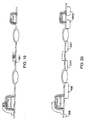
- a high quality thermal oxide 1801 is grown on the wafer surface to a thickness which depends upon the desired thickness of the gate oxide to be employed in the low voltage CMOS oxide transistor.
- a typical range of thicknesses for oxide layer 1801 would be 90 to 100 Angstroms for 3.6V systems.
- a polysilicon layer 1802 is deposited on top of the thermal oxide 1801 to a preferred thickness of 2500 Angstroms.
- polysilicon layer 1802 is patterned and etched to define the outer edges of word line gate 801. Notice that the low voltage CMOS transistor gate 1901 is also defined by the etching of polysilicon layer 1802 and that oxide 1801 provides the gate oxide for the low voltage CMOS transistor.
- low voltage diffusions 2001 and high voltage diffusions 2002 are used to form low voltage diffusions 2001 and high voltage diffusions 2002. This is accomplished using the same techniques described in the manufacture of the first embodiment with reference to FIG. 6 . Where the low voltage diffusion appears adjacent to word line gate 801 it is referred to as bit line diffusion 805. Where the high voltage diffusion appears adjacent to floating gate 804 it is referred to as source diffusion 806. Once the formation of both low voltage diffusions 2001 and high voltage diffusions 2002 are completed, standard processing techniques are used to finish the manufacture of the device to make a fully functional circuit.
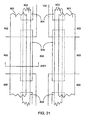
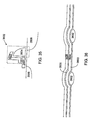
- FIG. 21 shows a top down view of two cells after performing the processes disclosed with reference to Figs. 9 through 20 .
- the cross sectional vantage point shown in FIG. 8 is denoted 2101.
- Potential advantages of the second embodiment are low costs of manufacture using a unique cell layout and a unique execution of standard CMOS manufacturing methods.
- the ability to control the floating gate to erase control gate coupling ratio is provided.
- the floating gate and erase control gate are made using a self-aligned process method that insures precise control of erase control gate coupling.
- An additional advantage is the independent control of all critical oxide thicknesses for transistors: floating gate, low voltage CMOS and high voltage CMOS.
- the layout and manufacturing methods will also support the optimization of the cell for interpoly erasure or erasure to the source
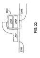
- FIG. 22 A second embodiment of memory cell in accordance with the present invention is shown in FIG. 22 .
- the cell in FIG. 22 is comprised, as in the first embodiment, of two transistors in series, namely a word line gate transistor 2201 and a storage transistor 2202.
- Storage transistor 2202 further consists of an erase control gate 2203 and a floating gate 2204. Diffused regions appear on the outside edges of the two transistors which constitute a bit line diffusions 2205 and a source diffusion 2206.
- the memory cell shown in FIG. 22 can be made by executing the sequence of steps disclosed with reference to Figs. 23 through 33 .
- field oxide regions 2302 are thermally grown in a lightly p-doped silicon crystalline substrate 2301.
- a high quality thermal oxide 2303 is grown on the wafer surface to a preferred thickness of 100 to 120 Angstroms.
- a first layer of polysilicon 2304 is deposited on the wafer surface to a preferred thickness of 500 Angstroms.
- polysilicon 2304 is patterned and etched using traditional photolithography methods.
- FIG. 24B a top view is shown of the cross sectional structure shown in FIG. 24A , which is marked by vantage point 24B01. Notice that polysilicon layer 2304 has had slots etched into it where it lies over oxide 2302 in the array by the photolithography step described with reference to FIG. 24A .
- the wafer is cleaned and a high quality thermal interpoly oxide 2501 is grown on the surface of the wafer to a preferred thickness of 200 through 400 Angstroms.
- a deposited oxide, oxynitride, or an oxide-nitride-oxide sandwich may also be used for oxide 2501.
- a second layer of polysilican 2502 is deposited on the surface of the wafer to a preferred thickness of 2000 Angstroms.
- polysilicon layer 2502 is patterned and etched along with underlying interpoly oxide 2501 and polysilicon layer 2304 are anisotropically etched. It is preferred to etch polysilicon 2502, interpoly oxide 2501 and polysilicon 2304 individually using a dry plasma etch. Notice that this etching step defines the outer edges of both floating gate 2204 and erase control gate 2203. Notice also that the peripheral areas which will eventually contain the high voltage CMOS transistors are protected during the etching processes by photoresist during this patterning and etching process.
- polysilicon layer 2502 is patterned and etched to form a high voltage CMOS transistor gate 2701.
- Interpoly oxide 2501 provides the gate oxide for the high voltage CMOS transistor 2701.
- the array area transistors are protected by photoresist during this patterning and etching process.
- a thermal oxide 2801 is grown on the surface of the wafer to a preferable thickness of 250 through 500 Angstroms. It is preferred to grow the oxide in a steam ambient as this will reduce the amount of time that the device spends at higher temperatures.
- dielectric spacers 2901 have been formed on the sides of floating gate 2204. This process is the same as is used in the second embodiment described with reference to FIG. 16 .
- Dielectric spacers 2901 protect the floating gate edge from chemical attack.
- a high quality thermal oxide 3101 is grown on the surface of the wafer to a preferred thickness of 90 Angstroms. Then, a third layer of polysilicon 3102 is deposited on the wafer to an appropriate thickness of approximately 2000 to 2500 Angstroms.
- polysilicon 3102 is patterned and etched in accordance with standard photolithography techniques. This etch defines the word line gate 2204.
- Low voltage CMOS transistor gate 3201 is also defined by the etching of polysilicon 3102, and oxide 3101 forms the gate oxide for the low voltage CMOS transistor.
- low voltage diffusions 3301 and high voltage diffusions 3302. This accomplished using the same techniques described in the manufacture of the first embodiment as described with reference to FIG. 6 .
- bit line diffusion 2205 Where the high voltage diffusion appears adjacent to floating gate 2204 it is referred to as source diffusion 2206.
- FIG. 34 shows a top down view of two cells after performing the processes described with reference to Figs. 23 through 33 .
- the cross sectional vantage point shown in FIG. 22 is denoted 3401.
- Advantages of the third embodiment include low cost manufacture of a high performance three gate cell using a unique cell layout and unique execution of standard CMOS manufacturing methods.
- the floating gate and erase control gate are made in a self aligned process that insures that the floating gate and erase gate are the same size.
- the second embodiment supports low risk salacide formation on both the source and drain of the device. Source resistance is greatly reduced if salacide formation is allowed on the source which improves overall circuit performance.
- the processing costs are lower than the second embodiment previously described.
- this embodiment allows for independent oxide control for all critical thin oxides: floating gate oxide, low voltage CMOS oxide, and high voltage CMOS oxide.
- FIG. 35 A third embodiment of a memory cell in accordance with the present invention is shown in FIG. 35 .
- the cell in FIG. 35 is comprised, as in the first embodiment, of two transistors in series, namely a word line gate transistor 3501 and a storage transistor 3502.
- Storage transistor 3502 further consists of an erase control gate 3503 and a floating gate 3504. Diffused regions appear on the outside edges of the two transistors which constitute bit line diffusion 3505 and source diffusion 3506.
- the memory cell shown in FIG. 35 can be made by executing the sequence of steps disclosed with reference to FIG. 36 through 44 .
- field oxide regions 3602 are thermally grown in a lightly p-doped silicon crystalline substrate 3601.
- a high quality thermal oxide 3603 is grown on the wafer surface to a thickness which depends upon the desired thickness of the gate oxide to be employed in the low voltage CMOS transistors.
- a typical preferred thickness for oxide 3601 would be 90 Angstroms for 3.3V operation.
- a first layer of polysilicon 3604 is deposited on the wafer surface to a preferred thickness of 2000 to 3000 Angstroms.
- an oxide 3605 is deposited on top of the polysilicon 3604 to a preferable thickness of 500 to 1000 Angstroms.
- an silicon nitride 3606 is deposited on top of the oxide 3605 to a thickness which will ultimately depend on the desired amount of coupling between erase control gate 3503 and floating gate 3504, which will be formed in later steps.
- a nominal thickness for nitride 3606 would be 2000 Angstroms.
- a thicker nitride 3606 would produce higher coupling by ultimately increasing the overlap area between erase control gate 3503 and floating gate 3504.
- nitride 3606, oxide 3605, and polysilicon 3604 are patterned and etched using traditional photolithography techniques leaving the structure shown. Note that the etching of nitride 3606, oxide 3605, and polysilicon 3604 are preferably performed using distinct etchants to remove these layers one at a time. Where the polysilicon 3604 is etched defines the outer edges of word line 3501 and low voltage CMOS transistor gate 3701.
- an oxide 3801 is thermally grown on the sides of polysilicon 3604 to a preferred thickness of 100 Angstroms. Nitride 3606 will not oxidize and thus oxide 3801 is not present on it.
- dielectric spacers 3802 are formed on the sides of word line 3501 and overlying layers. This process is the same as is used in the second embodiment described with reference to FIG. 16 .
- Dielectric spacers 3802 protect the floating gate edge from chemical attack.
- a high quality thermal oxide 4001 is grown on the surface of the wafer to a preferred thickness of 100 through 150 Angstroms. Oxide 4001 will contact the oxide underneath the floating gate 3504. Nitride 3606 will not oxidize and thus oxide 4001 is not present on it.
- a second polysilicon layer 4002 is deposited on the wafer surface to a preferred maximum thickness of 4000 Angstroms. Polysilicon layer 4002 will be used to form a floating gate which is self aligned to the word line gate 3501.
- the second polysilicon 4002 is anisotropically etched to form polysilicon spacers 4101 which will ultimately act as the floating gate 3504.
- portions of the remaining polysilicon spacers are masked and etched using well known lithography techniques.
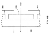
- FIG. 41B a top down view shows the location of word line 3501 and those portions of polysilicon spacers 4101 that remain after this second masked spacer etch. After the etch is completed and the photoresist removed, the cross section of the cell taken from vantage point 41B01 is shown in FIG. 41C .
- the effect of the etch is to remove to polysilicon spacers 4101 where they are not desired (e.g., on one half of the cell and from the sides of the voltage CMOS transistors 3701) and also to define the third and fourth sides of floating gate 3504 as seen in FIG. 41B .
- the remaining nitride 3606 is removed using hot phosphoric acid.
- the wafer is cleaned and an interpoly oxide 4201 is grown or deposited by CVD on the surface of the wafer to a preferred thickness of 300 Angstroms. Notice that in this embodiment the edge seal techniques used in the second and third embodiments are not required because the interpoly oxide will be substantially thicker than the oxide already present on the wafer.
- a third layer of polysilicon 4202 is deposited on the surface of the wafer to a preferred thickness of 2500 Angstroms.
- third polysilicon layer 4202 is patterned and etched to define the outer edges of erase control gates 3503.
- High voltage CMOS transistor gate 4301 is also defined by the etching of polysilicon 4202 and interpoly oxide 4201 provides the gate oxide for high voltage transistor 4301.
- low voltage diffusions 4401 and high voltage diffusions 4402. This accomplished using the same techniques described in the manufacture of the first embodiment described with reference to FIG. 6 .
- bit line diffusion 3505 Where the high voltage diffusion appears adjacent to floating gate 3504 it is referred to as source diffusion 3506.
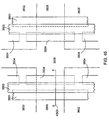
- FIG. 45 shows a top down view of two cells after performing the processes described with reference to Figs. 36 through 44 .
- the cross sectional vantage point shown in FIG. 35 is denoted 4501.
- Advantages of the fourth embodiment include: compatibility with deep submicron CMOS manufacturing methods and therefore scalability to achieve very high density layouts; the word line gate and the floating gate are self aligned to eliminate changes in read channel length from layer to layer misalignment; the floating gate size may be controlled with extreme precision due to the novel manufacturing method described; the cell has the smallest size and ease of scaling to very small dimensions when compared to other embodiments; and optional steps allow additional control of the area of the floating gate to erase gate coupling across the interpoly oxide.
- this will quicken the rate of oxidation of these layers when compared to the rate of growth on the lightly doped crystalline substrate.
- silicidation processes may be used to form a metallic silicide or salicide over exposed polysilicon and diffusion regions for the purpose of promoting faster signal transmission through these layers.
- cell be affected during processing by changing dielectric thicknesses, dielectric constants, overlap areas, and generally by optimizing the alignment of the various gates with respect to one another.
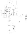
- FIG. 46A shows the conditions that can be applied to the cell to erase the cell. Erasure is accomplished by applying a positive bias to the erase control gate 103 the range of twelve to eighteen volts while holding substrate 107, bit line diffusion 105, and source diffusion 106 at ground.
- the interpoly oxide 402 thickness, oxide 203 thickness, and the geometric arrangement of the overlap of floating gate 104 and erase control gate 103 are chosen to allow the floating gate potential to tightly couple to ground relative to the erase gate.
- an effective electric field of about 8.5 megavolts/centimeter can be applied across interpoly oxide 402 during erasure.
- This high electric field allows electrons to tunnel via Fowler-Nordheim mechanics through interpoly oxide 402 from floating gates 104 to erase control gate 103. Using these conditions it will take anywhere in the range of one to 100 milliseconds to fully erase the cell.
- the polysilicon surfaces of floating gate 104 can be made rough where it is in contact with the interpoly oxide 402. This can be accomplished by adjusting the polysilicon deposition and doping conditions to change the resulting polysilicon grain sizes in the film that constitutes the floating gate 104. These asperites at the floating gate 104/interpoly oxide 402 interface will enhance the effective electric field in the interpoly oxide, thus facilitating erasure.
- the thickness of the interpoly oxide may be reduced to accentuate the electric field in that film, thus facilitating erasure.
- oxide reliability problems may result, such as oxide breakdown or unwanted charge transfer from the floating gate during the reading operation.
- floating gate 104 is left with a net positive charge which is suitable to provide for channel inversion 4601 in the silicon underneath floating gate 104 such that storage transistor 102 is normally "on” even absent a potential on the erase control gate.
- the disclosed biasing conditions are not the only way that erasure can be effectuated and that different biasing schemes can similarly achieve the desired result of leaving floating gate 104 with a net positive charge after erasure.
- the device may also be erased by Fowler-Nordheim tunneling of electrons through oxide 203 below the floating gate 104, through the application of a high voltage to source diffusion 106.
- source side erasure is a very popular technique in current Flash EPROM technologies.
- the claimed cell is not susceptible to overerasure because it envisions erasure resulting in a net positive charge being left on the floating gate. Such a condition would cause a systems failure in a traditional source side erase flash cell.
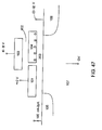
- FIG. 47 shows the conditions that can be applied to the cell to program the cell. Programming is accomplished by placing a high voltage on source diffusion 106 in the range of eleven to thirteen Volts, a moderately high voltage on erase control gate 103 in the range of six to eight Volts, and a relatively small voltage on word line gate 101 of about 2 Volts. Also, a current source is connected to bit line diffusion 105 which forces a current in the range of 100 nanoamperes to 2 microamperes. Substrate 107 is grounded.
- biasing conditions create a strong lateral electric field in substrate 107 underneath floating gate 104 such that the electrons in that region become "hot.” Because floating gate 104 during is coupled to a positive potential, some portion of these hot electrons will be drawn onto floating gate 104 thus programming the cell. Using these biasing conditions it will take anywhere in the range of 25 microseconds to 100 millisecond to program the device.
- programming speed may be reduced or the applied voltage during programming may be reduced by improving the coupling of high voltages to the floating gate during programming. Several ways to effectuate this desired result are described below.
- floating gate 104 After programming, floating gate 104 will be left with a net negative charge which causes further accumulation of positive charge carriers in the silicon underneath to floating gate such that no channel can be formed in that region absent biasing of erase control gate 103. Thus, a programmed cell is normally "off.”
- the disclosed biasing conditions are not the only way that programming can be effectuated and that different biasing schemes can similarly achieve the desired result of leaving floating gate 104 after programming with a net positive charge.
- the device may also be programmed by Fowler-Nordheim tunneling of electrons through oxide 203 below floating gate 104 through the application of a high voltage to erase control gate 103.
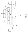
- FIG. 48 shows the conditions that are used to read the device, i.e., to detect if current is flowing between bit line diffusion 105 and source diffusion 106 to thus determine if the bit is at a logic one (and therefore erased) or zero (and therefore programmed). Reading is accomplished by placing the chip's power supply voltage, usually 5 volts, on both word line gate 101 and bit line diffusion 105. Source diffusion 106 and substrate 107 are grounded. Because the threshold voltage of word line gate 101 is lower than the applied word line gate voltage, a channel 4801 will form in substrate 107 underneath word line gate 101.
- bit line diffusion 105 and source diffusion 106 are no longer electrically isolated from one another, a substantial current will flow between them giving rise to a logic one state. Conversely, if the device is programmed, no channel will form underneath floating gate 104, and in fact channel formation is impeded in this region due to the net negative charge that exists on floating gate 104.
- bit line diffusion 105 and source diffusion 106 will not be electrically connected and will remain substantially electrically isolated from one another such that substantially no current will flow giving rise to a logic zero state.
- bit line diffusion 105 and source diffusion 106 will not be electrically connected and will remain substantially electrically isolated from one another such that substantially no current will flow giving rise to a logic zero state.
- the disclosed biasing conditions are not the only way that reading can be effectuated and that different biasing schemes can similarly achieve the desired result of detecting whether current can flow between bit line diffusion 105 and source diffusion 106.
- FIGS. 46A , 46B , 47 , and 48 most closely resemble the first embodiment shown in FIG. 1 , it should be clear to those of ordinary skill that the operational principles herein described will apply to all four embodiments.
- the disclosed three gate cell is believed to offer significant advantages over the prior art in that the "on" state current is substantially higher than alternate Flash cell configurations.
- Two examples of prior art cells are shown in Figs. 49A (the "SST” split gate cell) and 49B (the "ETOX” style cell).
- the oxide In the SST cell the oxide must remain relatively thick to withstand the higher voltages required for erasure.
- the ETOX cell because the word line gate is placed on top of the floating gate, the total effective oxide thickness between the word line gate and the substrate will again be thicker than is required underneath the word line in the claimed cell.
- the advantage of having a thinner oxide under the word line is that the claimed cell can achieve higher "on" state currents. The increased current allows the logic state of the cell to be determined more quickly by the sensing circuitry, and makes the claimed cell a better candidate over the prior art for high speed applications.
- a cell in accordance with the present invention can be made to be compatible with the CMOS circuitry that will exist outside of the array of cell. As described with reference to Figs. 2-6 , several of the processing steps used in the formation of the array are also used to build both high voltage and low voltage CMOS transistors. Thus, the claimed cell is a good candidate for embedded flash applications where it is desired to leave the exiting CMOS processes substantially intact. It is estimated that when a three gate cell in accordance with the present invention is added to a conventional CMOS technology that there will be only about a 30% increase in manufacturing costs, depending of course on which of the embodiments disclosed herein are utilized. Moreover, a cell in accordance with the present invention can be made very small and is optimal for use in high density flash applications.
- the design of the three gate Flash memory cell for high performance operation should insure reasonable erase and programming voltages and times. What is reasonable is a function of the application and engineering trade offs in the manufacturing process.
- the three gate Flash cell concept is flexible to allow optimization for a range of product and manufacturing constraints and will always yield high read current. For example, one-time-programming applications or high speed and density requirement may dictate the design engineer of the three gate cell to select a process that favors lower voltage operation in return for slower program and erase. For applications which require faster revision of the Flash memory contents, high voltages for that thus rapid programming and erasure will be designed into the specifics of the implementation.
- the three gate Flash cell in accordance with the present invention allows operation at reasonable voltages for program and erase which can be integrated with high performance CMOS at reasonable costs.
- the user of the cell can also choose to trade increased program and erase time during operation in return for slightly lower operational voltages. This can be achieved by changing the coupling capacitance between the floating gate and other voltage nodes in the cell. For example, to increase the programming speed, the floating gate must be coupled to a higher potential than the underlying channel to attract the hot electrons for capture. Increased coupling is accomplished by increasing the source diffusion to floating gate overlap, thus allowing more of the source voltage to be coupled onto the floating gate.
- programming simulations show that if the floating gate is coupled to 9 to 10 Volts that programming will be fast, taking typically about 25 to 100 microseconds.
- the disclosed programming method is efficient in that very low currents are required for fast programming, requiring currents of only about 0.5 microamps per cell. This means that power consumption during the programming operation is modest and allows programming to take place in systems that are powered by batteries.
- Vfg Vsource * Cprogram
- source side injection of hot electrons is difficult to predict, (see M. Kamiya, Y. Kojima, Yi Kato, K. Tanaka, and Y. Hayashi, "EEPROM Cell with high Gate Injection Efficiency", IEDM Tech.
- Csf the source diffusion to floating gate capacitance
- Cprogram is large when the term Csf is large and the other capacitance terms are small.
- Csf can be made large by having a thin dielectric under the floating gate and a sufficient overlap of the floating gate over the source diffusion. While it is desired that Cwf be small, it will necessarily be a factor because of the close vicinity of the word line gate and the floating gate.
- Minimization of Cef is restricted by consideration of the desirable erase voltage. If Cef is reduced by increasing the dielectric thickness between the erase gate and floating gate, it will consequently be harder to erase the device. However, Cef can be kept low by using minimum area of overlap between the erase control gate and the floating gate.
- the erase control gate voltage, Vec can also be optimized during programming to affect programming speed.
- the above analysis assumes that Vec is at ground, which tends to hold Vfg to lower voltages due to coupling between the erase control gate and the floating gate. However, if Vec is increased, Vfg will correspondingly increase, which, as noted above, will increase programming speed. Care must be taken to choose Vec such that the cell will not be erased. Balancing these consideration, an optimal Vec for fast programming should be approximately 6 to 8 Volts.
- Vec bias alleviates the need to have a greater floating gate to source diffusion overlap, thus making the cell more easily scaleable to smaller sizes; the potential applied to the source diffusion may be reduced which allows the junction and floating gate to be scaled to smaller dimensions; and Vec can be used to overcome the negative impact on programming operation when thinner interpoly oxides are required to optimize erasure.
- Erasure of the device occurs when electrons tunnel off of the floating gate as governed by the Fowler-Nordheim tunneling, a phenomenon well known in the art. It should be clear to those of ordinary skill that the three gate cells could be optimized for erasure by tunneling through the interpoly oxide (requiring low coupling from floating gate to control gate) or by tunneling from the floating gate through the underlying oxide to the source (requiring high coupling from floating gate to control gate).
- the potential for interpoly erasure is established by biasing the erase control gate to a high positive potential while setting all other nodes in the cell to ground.
- the erase control gate voltage necessary to achieve this field strength is determined to a first order by the thickness of the interpoly oxide and also by the amount of coupling of voltage onto the floating gate.
- tight coupling of the floating gate to the ground potential of the substrate is desirable so that most of the erase control gate voltage will appear across the interpoly oxide. If the potential that forms across the interpoly oxide when divided by the interpoly thickness exceeds 8.5 Megavolts/cm, electrons will be sufficiently able to tunnel and erase times will accordingly be reasonable.
- FIG. 46B illustrates this operational mode for the three gate cell.
- the erase control gate 103 and word line gate 101 are grounded with a high coupling between the erase control gate 103 and the floating gate 104.
- the overlap between the source diffusion and the floating gate would be reduced in this type of cell optimization to minimize coupling to the source.
- erase voltages i.e., storage transistor threshold voltages
- storage transistor threshold voltages storage transistor threshold voltages
- the three gate cell will need to be optimized for a given manufacturing facility to provide the desired erase time or erase control gate voltage. Interpoly oxide thickness between 100 to 500 Angstroms will yield practical erase voltages and still allow charge to be retained on the floating gate during storage and reading of the memory.
- a strong advantage of the three gate cell disclosed herein is that a wide distributions of erase voltages and effective interpoly oxide variations will produce acceptable operation of the cell.
- biasing the erase control gate can have certain advantages during programming.
Landscapes
- Engineering & Computer Science (AREA)
- Manufacturing & Machinery (AREA)
- Non-Volatile Memory (AREA)
- Semiconductor Memories (AREA)
- Metal-Oxide And Bipolar Metal-Oxide Semiconductor Integrated Circuits (AREA)
Description
- This invention relates generally to the field of integrated circuit devices, and more particularly relates to an integrated circuit device having embedded flash memory therein and to a method of manufacturing such a device.
- Non-volatile memory devices are an important and growing segment of the electronics industry. Non-volatile memory devices retain data or program information without the sustained application of power to the device. Electrically reprogrammable non-volatile memory devices allow the user to change the contents of the memory and retain that information after power is removed from the device: examples are electrically-erasable programmable read-only memory (EEPROM), and flash memory. Flash memory circuits enjoy lower costs than EEPROM since the number of transistors required to execute the memory function is reduced by a configuration which erases large (more than one bit) blocks of the memory in parallel or in a "flash."
- Flash memory is a very rapidly growing segment of the microelectronics industry with applications in almost all types of electronic products and systems. For mass memory applications the cost of the memory function is very important. Increasingly, flash memory is employed in what has been termed "embedded" applications where the nonvolatile memory function is incorporated into some other kind of chip, such as a microcontroller, digital signal processor (DSP), disc drive controller, or the like. This embedded approach can improve overall system performance, reduce size and costs by eliminating the need for two separate chips.
- Flash memory devices have increased value added in these embedded or highly integrated applications. However, traditional flash memory devices and manufacturing methods present challenges for embedded applications. Typical flash memory cells switch information more slowly than similar CMOS ROM cells. This means that either flash memory must be supplemented by faster-switching volatile memory or the system performance must be slowed to the point where flash memory can keep up. In addition many flash memory devices require greater than 30% increases in manufacturing steps when compared to typical CMOS devices.
- A flash memory device which offers high performance in switching speed with rates close to that of standard CMOS would be of great benefit to embedded applications. Two significant embedded applications where flash memory speed directly affects throughput or chip speed are DSP and microcontrollers.
Further devices are known fromWO 94/10706 US 5455792 . - In view of the foregoing, the present invention as claimed in claim1 relates to a electrically-alterable non-volatile information storage device with applications in data, program storage and the manufacture of programmable logic. The disclosed devices are well-suited to "flash" memory applications in which data is written for storage as bits, bytes, or pages but which is generally erased for rewriting in larger blocks of memory.
- The disclosed memory device allows the use of flash memory in higher-speed applications enabling new types of useful electronic circuits and systems. The invention consists of a higher performance cell with merged floating gate and control gate. The higher performance capability of this flash cell device is achieved at low cost by the disclosed cell's unique architecture by using the disclosed methods. The cell design and manufacturing methods allow the use of thin dielectrics to gate the conduction channel of the device, thus enabling higher on current performance. The memory device in accordance with the present invention functions in all current applications for flash memory and is cost competitive in manufacture. However, the memory device in accordance with the present invention offers significant improvements in performance over competing technologies. The higher performance of this novel device would allow the direct use of the memory transistor in high speed applications, whereas a lower performance traditional non-volatile memory transistor would require that the information from the non-volatile device be transferred to static RAM or other type of volatile storage having higher switching speed than traditional non-volatile memories.
- The excellent switching properties, low off current and high on current of a device in accordance with the present invention also allows it to be employed to replace EEPROM, fuses, anti-fuses or other electrically-alterable non-volatile switching devices in programmable logic devices.
- The memory device in accordance with the present invention can be fabricated with low cost methods. Numerous practical low cost alternative manufacturing flows are disclosed herein to build the new memory device. Unique cell layout and process sequences are defined for each basic method. A method to make self aligned cuts in polysilicon is used in one of the alternative methods of manufacture not forming part of the claimed invention. The manufacturing methods in accordance with the present invention are compatible with current tools and procedures, allowing the memory device in accordance with the invention to be added to CMOS circuits to replace masked ROM with more flexible Flash memory at a modest increase in cost.
- The cell operational method and manufacturing methods in accordance with the present invention allow the size of this memory element to be scaled smaller to maintain a low cost and high performance as the minimum feature size of microelectronic circuits is reduced in the future. The disclosed cell approach also offers simpler programming methods to simplify memory array design, supports higher cell currents for high speed applications and uses lower cost manufacturing methods than the more common "ETOX" cell approach. Furthermore, a new etching technique is disclosed which can used in the manufacture of the disclosed cell which allows a very thin gap to be etched in a polysilicon layer. In addition, novel process methods are disclosed that enable the cell to be manufactured in a practical manner by allowing thin dielectrics layers which are formed early in the process to be protected while dielectric is removed in other locations.
- The memory device in accordance with the present invention can be used for both embedded and stand-alone applications. The inherent switching speed of a device in accordance with the present invention can be about 200% (or more) faster than typical flash memory devices. The manufacture of this device is compatible with conventional CMOS process technologies and requires only about 25% increase in the number of manufacturing steps to add flash memory devices to a CMOS process.
- The high performance and modest cost of a memory device in accordance with the present invention allows it to be used in many high and low performance applications.
- Applications of the present invention can range from high-speed non volatile memory embedded within another type of integrated circuit, to high performance non-volatile switches in programmable logic devices. A cell in accordance with the present invention could also be used competitively for low speed mass memory applications.
- The foregoing and other features of the present invention may perhaps be best understood with reference to a detailed description of specific embodiments of the invention, which follows, when read in conjunction with the accompanying drawings, wherein:
-
FIG. 1 is a cross section of a silicon substrate showing a comparative example of a memory cell. -
FIG. 2 is a cross section of a silicon substrate showing the resulting structure after first polysilicon deposition. -
FIG. 3A is a cross section of a silicon substrate showing the remaining location of first polysilicon after etching. -
FIG. 3B is a cross section of a silicon substrate showing a pattered layer of nitride over the first polysilicon. -
FIG. 3C is a cross section of a silicon substrate showing where the polysilicon has been oxidized in the location where the overlying nitride has been etched away. -
FIG. 3D is a cross section of a silicon substrate showing the remaining structure when the nitride is slightly isotropically etched. -
FIG. 3E is a cross section of a silicon substrate showing the structure after anisotropic etching of the now exposed polysilicon. -
FIG. 3F is a cross section of a silicon substrate showing the structure after nitride removal and after a photoresist has been patterned on top of the polysilicon. -
FIG. 3G is a cross section of a silicon substrate showing the remaining structure after anisotropic etching of the exposed polysilicon. -
FIG. 3H is a planar view of the structure shown in cross section inFIG. 3A . -
FIG. 4 is a cross section of a silicon substrate showing the resulting structure after second polysilicon deposition. -
FIG. 5 is a cross section of a silicon substrate showing the remaining location of first polysilicon after etching. -
FIG. 6 is a cross section of a silicon substrate showing the position of the diffusion regions after ion implantation. -
FIG. 7 is a planar view of two completed cells in an array after the processes described inFigs. 2 through 6 have been completed. -
FIG. 8 is a cross section of a silicon substrate showing an embodiment of the claimed memory cell. -
FIG. 9 is a cross section of a silicon substrate showing resulting structure after polysilicon deposition. -
FIG. 10A is a cross section of a silicon substrate showing the remaining location of first polysilicon after etching. -
FIG. 10B is a planar view of the structure shown in cross section inFIG. 10A . -
Fig 11 is a cross section of a silicon substrate showing the resulting structure after interpoly oxide growth, second polysilicon deposition, oxide deposition, and nitride deposition. -
FIG. 12 is a cross section of a silicon substrate showing the remaining location f the oxide, nitride, and second polysilicon after these layers are etched. -
FIG. 13 is a cross section of a silicon substrate showing the resulting structure after oxide spacers are formed. -
FIG. 14 is a cross section of a silicon substrate showing the resulting structure after remaining exposed first polysilicon is etched. -
FIG. 15 is a cross section of a silicon substrate showing the resulting structure after the second polysilicon is etched to define the high voltage transistor gates. -
FIG. 16 is a cross section of a silicon substrate showing the resulting structure after the formation of dielectric spacers. -
FIG. 17 is a cross section of a silicon substrate showing the resulting structure after the removal of all oxides from the exposed surface of the substrate. -
FIG. 18 is a cross section f a silicon substrate showing the resulting structure after third polysilicon deposition. -
FIG. 19 is a cross section of a silicon substrate showing the remaining location of third polysilicon after etching. -
FIG. 20 is a cross section of a silicon substrate showing the position of the diffusion regions after ion implantation. -
FIG. 21 is a planar view of two completed cells in an array after the processes described inFigs. 9 through 20 have been completed. -
FIG. 22 is a cross section of a silicon substrate showing an embodiment of the claimed memory cell. -
FIG. 23 is a cross section of a silicon substrate showing the resulting structure after first polysilicon deposition. -
FIG. 24A is a cross section of a silicon substrate showing the remaining location of first polysilicon after etching. -
FIG. 24B is a planar view of the structure shown in cross section inFIG. 24A . -
FIG. 25 is a cross section of a silicon substrate showing the resulting structure after second polysilicon deposition. -
FIG. 26 is a cross section of a silicon substrate showing the resulting structure after the second polysilicon, interpoly oxide, and first polysilicon are etched. -
FIG. 27 is a cross section of a silicon substrate showing the resulting structure after the second polysilicon is etched to define the high voltage transistor gates. -
FIG. 28 is a cross section of a silicon substrate showing the resulting structure after thermal oxidation. -
FIG. 29 is a cross section of a silicon substrate showing the resulting structure after the formation of dielectric spacers. -
FIG. 30 is a cross section of a silicon substrate showing the resulting structure after all oxides are removed from the exposed surface of the substrate. -
FIG. 31 is a cross section of a silicon substrate showing the resulting structure after third polysilicon deposition. -
FIG. 32 is a cross section of a silicon substrate showing the remaining location of third polysilicon after etching. -
FIG. 33 is a cross section of a silicon substrate showing the position of the diffusion regions after ion implantation. -
FIG. 34 is a planar view of two completed cells in an array after the processes described inFigs. 23 through 33 have been completed. -
FIG. 35 is a cross section of a silicon substrate showing an embodiment of the claimed memory cell. -
FIG. 36 is a cross section of a silicon substrate showing the resulting structure after growth of a thermal oxide and the deposition of first polysilicon, oxide, and nitride. -
FIG. 37 is a cross section of a silicon substrate showing the remaining location of the nitride, oxide, and first polysilicon after etching of those layers. -
FIG. 38 is a cross section of a silicon substrate showing the resulting structure after the formation of dielectric spacers. -
FIG. 39 is a cross section of a silicon substrate showing the resulting structure after all oxides are removed from the exposed surface of the substrate. -
FIG. 40 is a cross section of a silicon substrate showing the resulting structure after second polysilicon deposition. -
FIG. 41A is a cross section of a silicon substrate showing the resulting structure after the formation of polysilicon spacers. -
FIG. 41B is a planar view of the structure shown in cross section inFIG. 24A after portions of the polysilicon spacers have been removed by etching. -
FIG. 41C is a cross section of a silicon substrate of the structure shown inFIG. 41B . -
FIG. 42 is a cross section of a silicon substrate of the resulting structure after third polysilicon deposition. -
FIG. 43 is a cross section of a silicon substrate showing the remaining location of third polysilicon after etching. -
FIG. 44 is a cross section of a silicon substrate showing the position of the diffusion regions after ion implantation. -
FIG. 45 is a planar view of two completed cells in an array after the processes described inFigs. 36 through 44 have been completed. -
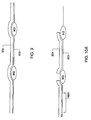
FIG. 46A is a cross section of a silicon substrate showing an embodiment of the claimed memory device and the biasing conditions that can be used to erase the device by causing charges to move through the interpoly oxide. -
FIG. 46B is a cross section of a silicon substrate showing an embodiment of the claimed memory device and the biasing conditions that can be used to erase the device by causing charges to move through the oxide underneath the floating gate. -
FIG. 47 is a cross section of a silicon substrate showing an embodiment of the claimed memory device and the biasing conditions that can be used to program the device. -
FIG. 48 is a cross section of a silicon substrate showing an embodiment of the claimed memory device and the biasing conditions that can be used to read the device. -
FIG. 49A is a cross section of a silicon substrate showing a prior art memory device called the "SST" cell. -
FIG. 49B is a cross section of a silicon substrate showing a prior art memory device called the "ETOX" cell. -
FIG. 50 is a cross section of a silicon substrate which shows the presence of the various capacitances that exists in the cell and that affect the programming and erasing operations. - The disclosed high performance Flash memory cell teaches a novel way to manufacture a split gate Flash memory cell in which each device contains a word line gate and a floating gate which sets the state of the cell. An erase control gate is provided to control potentials associated with program and erasure of the cells. High potentials required for programming and erase operations are applied to the erase control gate and do not directly appear across the word line gate or the floating gate. This feature allows the dielectrics employed for the word line gate to be thinner, since the word line gate will not need to withstand the higher programming and erase biases. The result is a higher on state current and a dense cell geometry. The practical realization of the memory cell requires the use of new process methods and unique process sequences which are described in the four embodiments of the invention described below. The method preferred for a given manufacturing plant will be influenced by available tooling and experience with specific methods needed for the realization of the three gate cell. Also, certain embodiments have certain performance advantages or may be more easily optimized to achieve desired results. Moreover, certain embodiments can be made more densely than other embodiments. Thus, which embodiment is preferred will depend on manufacturing, performance, and design constraints as noted herein. Furthermore, the desired or available power supply voltages and other desired electrical specifications for the cell may suggest that one embodiment will be more desirable than another.
- New process methods and novel process sequences are disclosed to enable the practical manufacture of the disclosed cell. Because the details of many of the processing steps are well known to those ordinarily skilled in semiconductor manufacturing, many of the processing details are not embellished upon. However, after the basic manufacturing flows of the four embodiments are described, and several well known processing techniques are described which have the potential to increase the performance of all of the embodiments.
- As well as showing the steps for forming the memory cell in the array area of the circuit, the cross sectional photos herein will also show how a low voltage CMOS (Complementary-Metal-Oxide-Semiconductor) transistor and a high voltage CMOS transistor can be built simultaneously in the periphery area of the circuit, thus underscoring the present invention's utility and manufacturing simplicity. The CMOS circuitry generally consists of all of the other circuitry used on the flash memory device that does not constitute the anay of cells, and performs circuit functions necessary to routing signals to and form the array, such as decoding. The low voltage CMOS transistors are used to perform logical functions are designed to handle nominal voltages signal (e.g., 5 Volts), while the high voltage CMOS transistors are used to shuttle higher voltage signals (e.g., 12 Volts) to the array to perform the erasing and programming functions. Because of the application of higher voltages to the high voltage CMOS transistors, these devices will typically require a thicker gate oxide thickness underneath their gates to prevent oxide wear out or breakdown. Also, the high voltage CMOS junctions will normally need to be deeper and more smoothly graded to sustain high voltages without going into avalanche breakdown. The layer thicknesses in the figures are not perfectly drawn to scale. The reader should consult the discussion accompanying the relevant figure in order to determine a layer's actual target thickness.
- A comparative example of a memory cell is shown in
FIG. 1 . The cell inFIG. 1 is comprised of two transistors in series, namely a wordline gate transistor 101 and astorage transistor 102.Storage transistor 102 further consists of an erasecontrol gate 103 and a floatinggate 104. Diffused regions appear on the outside edges of the two transistors which constitute abit line diffusion 105 and asource diffusion 106. The cell ofFIG. 1 would typically be built on a lightly doped p-type crystalline substrate 107. The memory cell shown inFIG. 1 can be made by executing the following sequence of steps, which can be best appreciated with reference to the cross-sectional diagrams ofFigs. 2 through 6 . - Referring to
FIG. 2 ,field oxide regions 202 are thermally grown in a lightly p-doped silicon crystalline substrate 201 for the purpose of electrically isolating different cells from one another and isolating the cells from the CMOS transistors in the periphery. A high qualitythermal oxide 203 is grown on the wafer surface to a thickness which depends upon the desired thickness of the gate oxide to be employed in the low voltage CMOS oxide transistor. A typical range of thicknesses foroxide layer 203 would be 120 to 150 Angstroms 10 Å = 1nm for 5.0V applications. Note thatoxide layer 203 is employed for both theword line gate 101 and thestorage gate 102. This offers significant advantages in that the wordline gate transistor 101 and thestorage transistor 102 both have high drive current afforded by the thin dielectric. Next apolysilicon layer 204 is deposited on top of thethermal oxide 203 to a preferred thickness of 2000 to 3000 Angstroms. - Referring to
FIG. 3A ,polysilicon layer 204 has been etched to define the outer edges ofword line gate 101 and floatinggate 104. Also, agap 301 has been anisotropically etched to define the inner edges ofword line gate 101 and floatinggate 104. Both the gap and the outer edges may be simultaneously patterned and etched using traditional photolithography processing methods. However, it is preferred to use the polysilicon etch method described inFIGS. 3B-3H to have the best cell operation. This method allows the self aligned formation of a gap in thepolysilicon 204 which is smaller than can be achieved with conventional lithography. This method supports effective hot electron programming of floatinggate 104 by source side injection and also provides a much smaller layout than could be achieved with conventional methods. - Referring to
FIG. 3B ,polysilicon 204 is covered with a nitride layer 3B01 to a preferred thickness of 2,000 to 4,000 Angstroms. The nitride layer is then patterned and etched by traditional means leaving the structure shown inFIG. 3B . Referring toFIG. 3C , which shows a magnified view of the nitride window etched inFIG. 3B , the exposedpolysilicon 204 is oxidized, forming an oxide layer 3C01 which is preferably 100 to 200 Angstroms thick. Notice that nitride layer 3B01 is not subject to oxidation. Referring toFIG. 3D , nitride 3B01 is subject to an isotropic etch to remove a very small amount of nitride 3B01 on all edges of nitride 3B01. The etchant used to remove the nitride should not substantially attack thepolysilicon 204 or oxide 3C01, and a solution of dilute hot phosphoric acid is suggested. Referring toFIG. 3E , thepolysilicon 204 is anisotropically etched where exposed. Where thepolysilicon 204 is protected by either nitride 3B01 or oxide 3C01, it will remain intact. Where the polysilicon is etched away, it formsgap 301 seen inFIG. 3A . Wherepolysilicon 204 is left unetched under oxide 3C01 constitutes the floatinggate 104. The remaining nitride 3B01 is then removed after etching thegap 301. Referring toFIG. 3F , a photoresist 3F01 is applied over thepolysilicon 204 and pattern, leaving the structure shown. Referring toFIG. 3G , the exposedpolysilicon 204 is anisotropically etched, and the photoresist 3F01 is then removed, leaving the structure shown. Notice that the oxide 3C01 has not been removed and will act to protect theunderlying polysilicon 204 from the anisotropic etch. Notice that this etch defines the outside edge of theword line 101 as well as the low voltageCMOS transistor gate 302.Oxide 203 acts as the gate oxide for the floatinggate 104, theword line gate 101, and the lowvoltage CMOS gate 302. - This etching technique used to form
gap 301 allows for the formation of an extremely thin gap inpolysilicon 204. The gap's thickness can be tightly controlled by controlling the etch rate of the overlying nitride 3C01. This technique has utility above that simply disclosed in formation of the above Flash EPROM cell. Because the gap that is produced is very thin, it can be used to form a series of transistor gates which do not require significant layout area for a diffusion or other connection between the gates to help jumper a signal through the gate series. A lower series resistance can be achieved by implanting dopants into the gap after the etch. However, in applications where a slightly higher resistance can be tolerated, no special implant or method is needed to allow the channel of thestorage gate 102 to communicate with theword line gate 101. This is because channel formation will naturally extend beyond the physical edge of the gate and can extend to touch the channel of the next gate in series if the gap is sufficiently narrow. In this way, very dense logic gates similar in function to charge-coupled-devices (CCDs) can be made. - Referring to
FIG. 3H , a top down view is shown of the cross sectional structure shown inFig 3A , which is marked by vantage point 3H01. Notice that the floatinggate 104 has been etched on four sides by the photolithography step discussed inFIG. 3A . - Referring to
FIG. 4 , the wafer is next subjected to oxidation to increase the thickness of the oxide on the exposed silicon surfaces to from the dielectrics for the high voltage transistors. The total oxide thickness should be about 250 to 400 Angstroms for best results. Whereoxide 401 appears over the floating gate it is referred to asinterpoly oxide 402.Oxide 401 should be grown to a thickness which will perform optimally when used as both an interpoly oxide and as the gate oxide for the high voltage CMOS transistors. A thickness of approximately 300 Angstroms is preferred. Next a second layer ofpolysilicon 403 is deposited on the surface of the wafer. - Referring to
FIG. 5 ,polysilicon layer 403 is patterned and anisotropically etched using traditional photolithography methods. This etch defines erasecontrol gate 103. Notice that high voltageCMOS transistor gate 501 is also defined by the etching ofpolysilicon layer 403 and thatoxide 401 provides the gate oxide for the high voltage CMOS transistor.Polysilicon layer 403 should be patterned to produce an erasecontrol gate 103 which overlaps with the underlying floatinggate 104 in order to optimize coupling between these two gates. - Referring to
FIG. 6 , standard processing techniques are used to formlow voltage diffusions 601 andhigh voltage diffusions 602. This is accomplished by first masking off the low voltage diffusion regions and performing an ion implantation step. The ion implantation step causes ions to bombard perpendicularly into the wafer surface. Where the ions become embedded into substrate 201 ahigh voltage diffusion 601 will be formed. The ions will be of a character (e.g., phosphorous or arsenic) to impart an n-type character to the substrate 201 in thehigh voltage diffusions 601. Because the low voltage regions are masked off, no ions will be implanted into the substrate 201 in those regions. After thehigh voltage diffusions 602 have been implanted, highvoltage diffusion regions 602 are then masked into order to ion implant thelow voltage diffusions 601 in the same manner as previously described. Notice that the ion implantation process and subsequent appropriate thermal drive of the ions are engineered such that thehigh voltage diffusions 602 are deeper and more smoothly graded than thelow voltage diffusions 601 and can therefore carry a higher voltage signal without breaking down. Where the low voltage diffusion appears adjacent toword line gate 101 it is referred to asbit line diffusion 105. Where the high voltage diffusion appears adjacent to floatinggate 104 it is referred to assource diffusion 106. Once the formation of bothlow voltage diffusions 601 andhigh voltage diffusions 602 are completed, standard processing techniques are used to finished the manufacture of the device to make a fully functional circuit. -
FIG. 7 shows a top down view of two cells after performing the processes described with reference toFigs. 2 through 6 . Notice that it is preferred to use the claimed memory cell in a common source configuration whereby each cell'ssource diffusion 106 is common to all other cells' source diffusion and each cell'sbit line diffusion 105 is shared with only one other cell's bit line diffusion. The vantage point shown inFIG. 1 is denoted by 701. Among the advantages of this first embodiment are higher density and lower costs due to the processing sequence that allows the self aligned formation of a floating gate and word line gate from the same layer of polysilicon. This lowers manufacturing costs, increases layout density, and allows greater flexibility in the selection of erase control gate to floating gate coupling ratio. Also, the thin gate oxides are formed first, and the interpoly oxide is formed with the floating gate and low voltage CMOS gates already defined. No additional processing steps are required to insure isolation between the floating gate and the word line gate. - A first embodiment of a memory cell in accordance with the present invention is shown in
FIG. 8 . The cell inFig. 8 is comprised, as in the first embodiment, of two transistors in series, namely a wordline gate transistor 801 and astorage transistor 802.Storage transistor 802 further consists of an erasecontrol gate 803 and a floatinggate 804. Diffused regions appear on the outside edges of the two transistors which con-mtutebit line diffusion 805 andsource diffusion 806. The memory cell shown inFIG. 8 can be made by executing the sequence of steps to be described with reference toFigs. 9 through 20 . - Referring to
FIG. 9 ,field oxide regions 902 are thermally grown in a lightly p-doped silicon crystalline substrate 901. Clearly, other field isolation methods such as shallow trench and refill may also be applied in lieu of lower cost local oxidation of silicon method. A high qualitythermal oxide 903 is grown on the wafer surface to a thickness of 100 Angstroms in a presently preferred embodiment. Next apolysilicon layer 904 is deposited on top ofthermal oxide 903 to a thickness of approximately 500 Angstroms in a presently preferred embodiment. - Referring to
FIG. 10A ,polysilicon layer 904 has been patterned and etched using traditional photolithography methods. Notice thatpolysilicon layer 904 has been left only in the array and will be used to form the floatinggate 804. Referring toFIG. 10B , a top view is shown of the cross sectional structure shown inFig 10A , which is marked by vantage point 10B01. Notice thatpolysilicon layer 904 has had slots etched into it where it lies overoxide 902 in the array by the photolithography step described with reference toFIG. 10A . - Referring to
FIG. 11 , after the exposed portions of substrate 901 are cleaned, a highquality interpoly oxide 1101 is formed. The preferred method is a combination of thermal oxidation followed by the deposition of oxide by Chemical Vapor Deposition (CVD). It is complicated to predict what method would be best. CVD oxide for part of the oxidation gives better control over the shape of the interpoly oxide and can reduce cell disturb problems. When polysilicon over field oxide is oxidized an inverse point can form which tends to cause field enhancement.Oxide 1101 can also be formed by only thermal oxidation which would in turn leave only about 250 Angstroms on the exposed portions of substrate 901 because doped polysilicon will oxidize faster than the lightly doped crystalline silicon. Next, a second layer ofpolysilicon 1102 is deposited on the surface of the wafer to preferred thickness of 2000 Angstroms. Then anoxide layer 1103 is formed on top ofpolysilicon 1102 to a preferred thickness of 400 Angstroms. Then silicon nitride (nitride) 1104 is deposited on top ofoxide 1103 to a preferred thickness of 500 to 1000 Angstroms. - Referring to
FIG. 12 ,nitride 1104,oxide 1103, andpolysilicon layer 1102 have been etched using traditional photolithography techniques to define the outer edges of erasecontrol gate 803. Because each of these layers requires the use of different etchants, each layer is etched separately using dry etching. - Referring to
Fig 13 , it is desired at this point to deposit aspacer oxide 1301 on the sides of the erasecontrol gate 803. While the spacer oxide formation process is not shown inFIG. 13 , it is known generally in the art and is explained only briefly. The spacer process preferably comprises depositing approximately 1000 to 2500 Angstroms of oxide or nitride over the structure inFIG. 12 , and subjecting the deposited oxide or nitride to an anisotropic dry etch which occurs perpendicular to the substrate 901. This etch will preferentially etch away the oxide overlying horizontal surfaces while leaving aspacer oxide 1301 covering the vertical surfaces. After the etch, thespacer oxide 1301 will remain and will be about 75% as thick on the side of the erasecontrol gate 803 as the original oxide or nitride film (e.g., 1000 to 2500 Angstroms in a preferred embodiment). Notice that the anisotropic etch is also used to removeinterpoly oxide 1101 from the top ofpolysilicon 904. While the spacer oxide will also form on the vertical edges of the structures overfield oxide 902, spacers in this location are unimportant and have not been drawn inFIG. 13 . - Referring to
FIG. 14 , the exposed portions ofpolysilicon 904 can be anisotropically etched using the overlying erasecontrol gate 803 andspacer oxide 1301 as a mask. This etching step defines the outer edges of floatinggate 804, thus self aligning floatinggate 804 underneath the erasecontrol gate 803. It is desirable to dry etch the polysilicon such thatnitride 1104 is not substantially thinned to protectoxide 1103 from being attacked during subsequent cleaning steps. Retaining a maximum amount ofoxide 1103 is desirable to minimize coupling between erasecontrol gate 803 andword line gate 801 which has yet to be formed. However, this is not required to successfully manufacture this cell and the nitride may instead be completely removed at this point. Note also that the remaining nitride must ultimately be removed prior to salacide formation or contact formation to be formed much later in the process flow. - Referring to
FIG. 15 , the remainingnitride 1104,oxide 1103, andpolysilicon 1102 in the high voltage CMOS area are patterned and etched using traditional photolithography methods. As described with reference toFIG. 12 , multi-step dry etching is used to remove these three materials individually. Notice that wherepolysilicon 1102 has been etched defines highvoltage CMOS gates 1501. Notice also thatinterpoly oxide 1101 provides the gate oxide for highvoltage CMOS transistor 1501. - Referring to
FIG. 16 , it is desired to protect theoxide 903 under the floatinggate 804 from subsequent chemical processing which is described with reference toFIG. 17 . This is referred to as edge sealing. To effectuate edge sealing, the cell is oxidized at this stage to form a thin layer ofoxide 1601 on the sides of the floatinggate 804 to a preferred thickness of 200 Angstroms. This oxide will grow to a lesser extent where oxides are already present and is shown inFIG. 16 only where it overlies a transistor structure. Becauseoxide layer 1601 will not be thick enough to adequately protect against subsequent chemical etching, it is desired to also putdielectric spacers 1602 on the sides of floatinggate 804. The general processing steps to form spacers are well known in the art and are described with reference toFIG. 13 .Dielectric spacers 1602 are also beneficial in that they will ultimately provide more insulation between floatinggate 804 and erasecontrol gate 803 fromword line gate 801 which has not yet been formed. The spacers can be made several different ways with different potential advantages and drawbacks. Nitride spacers, while the cheapest from a manufacturing standpoint, may suffer from the drawback that during use of the cell electrons may become trapped in the nitride spacer thus inadvertently hampering the ability of the device to form a channel. Therefore, if nitride spacers are used fordielectric spacer 1602, they should preferably be made a thinly as possible to leave 150 to 250 Angstroms of spacer on the side of the floating gate. Alternatively, an oxide spacer could be used. An acceptable oxide spacer can be achieved by oxidizing a pre-formed polysilicon spacer in a steam ambient. The thickness of the polysilicon spacer can be engineered such that it is completely oxidized when performing the subsequent high quality thermal oxidation process described with reference toFIG. 18 , which would be approximately 150 Angstroms thick on the side of floatinggate 804 prior to oxidation. - If it is inconvenient to optimize polysilicon deposition to match the subsequent oxidation step, the polysilicon can first be partially oxidized prior to the clean up described with reference to
FIG. 17 that proceeds the high quality thermal oxidation step. To implement this, approximately 300 Angstroms of polysilicon is left on the side of floatinggate 804, which is then be partially oxidized leaving approximately 180 Angstroms of the polysilicon spacer unoxidized. During the subsequent clean up step, the oxidized portion of the spacer is removed, leaving the 180 Angstroms or so of unoxidized polysilicon spacer. This remaining portion of the polysilicon spacer is subsequently oxidized during the high quality oxidation process described with reference toFIG. 18 . While the use of oxidized polysilicon spacers may be more expensive from a manufacturing standpoint, it is the presently preferred method because it can be expected to be superior in performance to nitride spacers; inadvertent trapping is minimized, while subsequent oxidation processes may be tailored independent of the edge sealing process described here. Although the dielectric spacers have been drawn inFIG. 16 such that they extend to the top of the vertical edges, they may in actuality extend only part of the way up the vertical edge; thedielectric spacers 1601 must extend at least far enough to cover the sides of the floatinggate 804. - Referring to
FIG. 17 , all oxides that have been formed on the exposed surfaces of substrate 901 are removed using a diluted solution of hydrofluoric acid. Notice that thedielectric spacers 1602 protect the floating gate edge and the oxide underneath the floating gate from chemical attack while the oxide is completely removed from the single crystal silicon surface. This edge sealing process thus allows the growth of a thin high quality oxide on the exposed areas whose thickness is independent of that used under the floating gate. - Referring to
FIG. 18 , a high qualitythermal oxide 1801 is grown on the wafer surface to a thickness which depends upon the desired thickness of the gate oxide to be employed in the low voltage CMOS oxide transistor. A typical range of thicknesses foroxide layer 1801 would be 90 to 100 Angstroms for 3.6V systems. Next apolysilicon layer 1802 is deposited on top of thethermal oxide 1801 to a preferred thickness of 2500 Angstroms. - Referring to
FIG. 19 ,polysilicon layer 1802 is patterned and etched to define the outer edges ofword line gate 801. Notice that the low voltageCMOS transistor gate 1901 is also defined by the etching ofpolysilicon layer 1802 and thatoxide 1801 provides the gate oxide for the low voltage CMOS transistor. - Referring to
FIG. 20 , standard processing techniques are used to formlow voltage diffusions 2001 andhigh voltage diffusions 2002. This is accomplished using the same techniques described in the manufacture of the first embodiment with reference toFIG. 6 . Where the low voltage diffusion appears adjacent toword line gate 801 it is referred to asbit line diffusion 805. Where the high voltage diffusion appears adjacent to floatinggate 804 it is referred to assource diffusion 806. Once the formation of bothlow voltage diffusions 2001 andhigh voltage diffusions 2002 are completed, standard processing techniques are used to finish the manufacture of the device to make a fully functional circuit. -
FIG. 21 shows a top down view of two cells after performing the processes disclosed with reference toFigs. 9 through 20 . The cross sectional vantage point shown inFIG. 8 is denoted 2101. Potential advantages of the second embodiment are low costs of manufacture using a unique cell layout and a unique execution of standard CMOS manufacturing methods. The ability to control the floating gate to erase control gate coupling ratio is provided. the floating gate and erase control gate are made using a self-aligned process method that insures precise control of erase control gate coupling. An additional advantage is the independent control of all critical oxide thicknesses for transistors: floating gate, low voltage CMOS and high voltage CMOS. The layout and manufacturing methods will also support the optimization of the cell for interpoly erasure or erasure to the source - A second embodiment of memory cell in accordance with the present invention is shown in
FIG. 22 . The cell inFIG. 22 is comprised, as in the first embodiment, of two transistors in series, namely a wordline gate transistor 2201 and astorage transistor 2202.Storage transistor 2202 further consists of an erasecontrol gate 2203 and a floatinggate 2204. Diffused regions appear on the outside edges of the two transistors which constitute abit line diffusions 2205 and asource diffusion 2206. The memory cell shown inFIG. 22 can be made by executing the sequence of steps disclosed with reference toFigs. 23 through 33 . - Referring to
FIG. 23 ,field oxide regions 2302 are thermally grown in a lightly p-doped silicon crystalline substrate 2301. A high qualitythermal oxide 2303 is grown on the wafer surface to a preferred thickness of 100 to 120 Angstroms. Then a first layer ofpolysilicon 2304 is deposited on the wafer surface to a preferred thickness of 500 Angstroms. - Referring to
FIG. 24A ,polysilicon 2304 is patterned and etched using traditional photolithography methods. Referring toFIG. 24B , a top view is shown of the cross sectional structure shown inFIG. 24A , which is marked by vantage point 24B01. Notice thatpolysilicon layer 2304 has had slots etched into it where it lies overoxide 2302 in the array by the photolithography step described with reference toFIG. 24A . - Referring to
FIG. 25 , the wafer is cleaned and a high qualitythermal interpoly oxide 2501 is grown on the surface of the wafer to a preferred thickness of 200 through 400 Angstroms. A deposited oxide, oxynitride, or an oxide-nitride-oxide sandwich may also be used foroxide 2501. Then a second layer ofpolysilican 2502 is deposited on the surface of the wafer to a preferred thickness of 2000 Angstroms. - Referring to
FIG. 26 ,polysilicon layer 2502 is patterned and etched along withunderlying interpoly oxide 2501 andpolysilicon layer 2304 are anisotropically etched. It is preferred to etchpolysilicon 2502,interpoly oxide 2501 andpolysilicon 2304 individually using a dry plasma etch. Notice that this etching step defines the outer edges of both floatinggate 2204 and erasecontrol gate 2203. Notice also that the peripheral areas which will eventually contain the high voltage CMOS transistors are protected during the etching processes by photoresist during this patterning and etching process. - Referring to
FIG. 27 ,polysilicon layer 2502 is patterned and etched to form a high voltageCMOS transistor gate 2701.Interpoly oxide 2501 provides the gate oxide for the highvoltage CMOS transistor 2701. The array area transistors are protected by photoresist during this patterning and etching process. - Referring to
FIG. 28 , athermal oxide 2801 is grown on the surface of the wafer to a preferable thickness of 250 through 500 Angstroms. It is preferred to grow the oxide in a steam ambient as this will reduce the amount of time that the device spends at higher temperatures. - Referring to
FIG. 29 ,dielectric spacers 2901 have been formed on the sides of floatinggate 2204. This process is the same as is used in the second embodiment described with reference toFIG. 16 . - Referring to
FIG. 30 , all oxides that have formed on the exposed surfaces of substrate 2301 are removed using a diluted solution of hydrofluoric acid.Dielectric spacers 2901 protect the floating gate edge from chemical attack. - Referring to
FIG. 31 , a high qualitythermal oxide 3101 is grown on the surface of the wafer to a preferred thickness of 90 Angstroms. Then, a third layer ofpolysilicon 3102 is deposited on the wafer to an appropriate thickness of approximately 2000 to 2500 Angstroms. - Referring to
FIG. 32 ,polysilicon 3102 is patterned and etched in accordance with standard photolithography techniques. This etch defines theword line gate 2204. Low voltageCMOS transistor gate 3201 is also defined by the etching ofpolysilicon 3102, andoxide 3101 forms the gate oxide for the low voltage CMOS transistor. - Referring to
FIG. 33 , standard processing techniques are used to formlow voltage diffusions 3301 andhigh voltage diffusions 3302. This accomplished using the same techniques described in the manufacture of the first embodiment as described with reference toFIG. 6 . Where the low voltage diffusion appears adjacent toword line gate 2201 it is referred to asbit line diffusion 2205. Where the high voltage diffusion appears adjacent to floatinggate 2204 it is referred to assource diffusion 2206. Once the formation of both thelow voltage diffusions 3301 andhigh voltage diffusions 3302 are completed, standard processing techniques are used to finish the manufacture of the device to make a fully functional circuit. -
FIG. 34 shows a top down view of two cells after performing the processes described with reference toFigs. 23 through 33 . The cross sectional vantage point shown inFIG. 22 is denoted 3401. Advantages of the third embodiment include low cost manufacture of a high performance three gate cell using a unique cell layout and unique execution of standard CMOS manufacturing methods. Also, the floating gate and erase control gate are made in a self aligned process that insures that the floating gate and erase gate are the same size. Moreover, the second embodiment supports low risk salacide formation on both the source and drain of the device. Source resistance is greatly reduced if salacide formation is allowed on the source which improves overall circuit performance. Furthermore, the processing costs are lower than the second embodiment previously described. Also, like the second embodiment, this embodiment allows for independent oxide control for all critical thin oxides: floating gate oxide, low voltage CMOS oxide, and high voltage CMOS oxide. - A third embodiment of a memory cell in accordance with the present invention is shown in
FIG. 35 . The cell inFIG. 35 is comprised, as in the first embodiment, of two transistors in series, namely a wordline gate transistor 3501 and astorage transistor 3502.Storage transistor 3502 further consists of an erasecontrol gate 3503 and a floatinggate 3504. Diffused regions appear on the outside edges of the two transistors which constitutebit line diffusion 3505 andsource diffusion 3506. The memory cell shown inFIG. 35 can be made by executing the sequence of steps disclosed with reference toFIG. 36 through 44 . - Referring to
FIG. 36 ,field oxide regions 3602 are thermally grown in a lightly p-doped silicon crystalline substrate 3601. A high qualitythermal oxide 3603 is grown on the wafer surface to a thickness which depends upon the desired thickness of the gate oxide to be employed in the low voltage CMOS transistors. A typical preferred thickness for oxide 3601 would be 90 Angstroms for 3.3V operation. Then a first layer ofpolysilicon 3604 is deposited on the wafer surface to a preferred thickness of 2000 to 3000 Angstroms. Next anoxide 3605 is deposited on top of thepolysilicon 3604 to a preferable thickness of 500 to 1000 Angstroms. Next ansilicon nitride 3606 is deposited on top of theoxide 3605 to a thickness which will ultimately depend on the desired amount of coupling between erasecontrol gate 3503 and floatinggate 3504, which will be formed in later steps. A nominal thickness fornitride 3606 would be 2000 Angstroms. Athicker nitride 3606 would produce higher coupling by ultimately increasing the overlap area between erasecontrol gate 3503 and floatinggate 3504. - Referring to
FIG. 37 ,nitride 3606,oxide 3605, andpolysilicon 3604 are patterned and etched using traditional photolithography techniques leaving the structure shown. Note that the etching ofnitride 3606,oxide 3605, andpolysilicon 3604 are preferably performed using distinct etchants to remove these layers one at a time. Where thepolysilicon 3604 is etched defines the outer edges ofword line 3501 and low voltageCMOS transistor gate 3701. - Referring to
FIG. 38 , anoxide 3801 is thermally grown on the sides ofpolysilicon 3604 to a preferred thickness of 100 Angstroms.Nitride 3606 will not oxidize and thusoxide 3801 is not present on it. Next,dielectric spacers 3802 are formed on the sides ofword line 3501 and overlying layers. This process is the same as is used in the second embodiment described with reference toFIG. 16 . - Referring to
FIG. 39 , all oxides that have formed on the exposed surfaces of substrate 3601 are removed using a diluted solution of hydrofluoric acid.Dielectric spacers 3802 protect the floating gate edge from chemical attack. - Referring to
FIG. 40 , a high qualitythermal oxide 4001 is grown on the surface of the wafer to a preferred thickness of 100 through 150 Angstroms.Oxide 4001 will contact the oxide underneath the floatinggate 3504.Nitride 3606 will not oxidize and thusoxide 4001 is not present on it. Next, asecond polysilicon layer 4002 is deposited on the wafer surface to a preferred maximum thickness of 4000 Angstroms.Polysilicon layer 4002 will be used to form a floating gate which is self aligned to theword line gate 3501. - Referring to
FIG. 41A , thesecond polysilicon 4002 is anisotropically etched to formpolysilicon spacers 4101 which will ultimately act as the floatinggate 3504. Next, portions of the remaining polysilicon spacers are masked and etched using well known lithography techniques. Referring toFIG. 41B , a top down view shows the location ofword line 3501 and those portions ofpolysilicon spacers 4101 that remain after this second masked spacer etch. After the etch is completed and the photoresist removed, the cross section of the cell taken from vantage point 41B01 is shown inFIG. 41C . Notice that the effect of the etch is to remove topolysilicon spacers 4101 where they are not desired (e.g., on one half of the cell and from the sides of the voltage CMOS transistors 3701) and also to define the third and fourth sides of floatinggate 3504 as seen inFIG. 41B . - Referring to
FIG. 42 , the remainingnitride 3606 is removed using hot phosphoric acid. Next, the wafer is cleaned and aninterpoly oxide 4201 is grown or deposited by CVD on the surface of the wafer to a preferred thickness of 300 Angstroms. Notice that in this embodiment the edge seal techniques used in the second and third embodiments are not required because the interpoly oxide will be substantially thicker than the oxide already present on the wafer. Next, a third layer ofpolysilicon 4202 is deposited on the surface of the wafer to a preferred thickness of 2500 Angstroms. - Referring to
FIG. 43 ,third polysilicon layer 4202 is patterned and etched to define the outer edges of erasecontrol gates 3503. High voltageCMOS transistor gate 4301 is also defined by the etching ofpolysilicon 4202 andinterpoly oxide 4201 provides the gate oxide forhigh voltage transistor 4301. - Referring to
FIG. 44 , standard processing techniques are used to formlow voltage diffusions 4401 andhigh voltage diffusions 4402. This accomplished using the same techniques described in the manufacture of the first embodiment described with reference toFIG. 6 . Where the low voltage diffusion appears adjacent toword line gate 3501 it is referred to asbit line diffusion 3505. Where the high voltage diffusion appears adjacent to floatinggate 3504 it is referred to assource diffusion 3506. Once the formation of bothlow voltage diffusions 4401 andhigh voltage diffusions 4402 are completed, standard processing techniques are used to finish the manufacture of the device to make a fully functional circuit. -
FIG. 45 shows a top down view of two cells after performing the processes described with reference toFigs. 36 through 44 . The cross sectional vantage point shown inFIG. 35 is denoted 4501. Advantages of the fourth embodiment include: compatibility with deep submicron CMOS manufacturing methods and therefore scalability to achieve very high density layouts; the word line gate and the floating gate are self aligned to eliminate changes in read channel length from layer to layer misalignment; the floating gate size may be controlled with extreme precision due to the novel manufacturing method described; the cell has the smallest size and ease of scaling to very small dimensions when compared to other embodiments; and optional steps allow additional control of the area of the floating gate to erase gate coupling across the interpoly oxide. - One of ordinary skill in the art of semiconductor processing will realize that there are many different ways to effectuate and optimized the embodiments described. For example, it may be beneficial prior to diffusion formation to form a spacer or sidewall oxide on the sides of the polysilicon for the purposes of reducing short channel effects and protecting the gate oxide layer from ion implant damage. The high quality dielectric used as gate oxides or as interpoly oxides could be made of thermal oxide, nitrided oxides, oxynitride, or even oxide-nitride sandwiches of various sorts. One of ordinary skill will also recognize that the polysilicon is generally doped either after deposition or during deposition for the purpose of decreasing the polysilicon's resistance and thus promoting faster signal transmission through these layers. In some cases, this will quicken the rate of oxidation of these layers when compared to the rate of growth on the lightly doped crystalline substrate. Also, silicidation processes may be used to form a metallic silicide or salicide over exposed polysilicon and diffusion regions for the purpose of promoting faster signal transmission through these layers. Furthermore, one of normal skill in the art will recognize that the various coupling requirements that are important to optimize cell performance, which will be described in detail later, cell be affected during processing by changing dielectric thicknesses, dielectric constants, overlap areas, and generally by optimizing the alignment of the various gates with respect to one another.
- Operating principles of devices in accordance with the present invention will now be described in reference to the comparative example of
FIG. 1 .FIG. 46A shows the conditions that can be applied to the cell to erase the cell. Erasure is accomplished by applying a positive bias to the erasecontrol gate 103 the range of twelve to eighteen volts while holdingsubstrate 107,bit line diffusion 105, andsource diffusion 106 at ground. Theinterpoly oxide 402 thickness,oxide 203 thickness, and the geometric arrangement of the overlap of floatinggate 104 and erasecontrol gate 103 are chosen to allow the floating gate potential to tightly couple to ground relative to the erase gate. Thus, an effective electric field of about 8.5 megavolts/centimeter can be applied acrossinterpoly oxide 402 during erasure. This high electric field allows electrons to tunnel via Fowler-Nordheim mechanics throughinterpoly oxide 402 from floatinggates 104 to erasecontrol gate 103. Using these conditions it will take anywhere in the range of one to 100 milliseconds to fully erase the cell. - One of ordinary skill in the art will realize that erase time can be reduced in several ways. First, the polysilicon surfaces of floating
gate 104 can be made rough where it is in contact with theinterpoly oxide 402. This can be accomplished by adjusting the polysilicon deposition and doping conditions to change the resulting polysilicon grain sizes in the film that constitutes the floatinggate 104. These asperites at the floatinggate 104/interpoly oxide 402 interface will enhance the effective electric field in the interpoly oxide, thus facilitating erasure. Second, the thickness of the interpoly oxide may be reduced to accentuate the electric field in that film, thus facilitating erasure. Of course, if the oxide is made too thin, oxide reliability problems may result, such as oxide breakdown or unwanted charge transfer from the floating gate during the reading operation. Third, proper geometric arrangement of the three gates with respect to one another may affect the coupling to produce a lower coupled voltage on floatinggate 104 and thus a higher voltage and field across the interpoly oxide which would facilitate erasure. Likewise, changing any of theses factors may also make it possible to lower the voltages needed to accomplish erasure in a reasonable amount of time. These details will be embellished upon below. - After erasure, floating
gate 104 is left with a net positive charge which is suitable to provide for channel inversion 4601 in the silicon underneath floatinggate 104 such thatstorage transistor 102 is normally "on" even absent a potential on the erase control gate. One of ordinary skill in the art will realize that the disclosed biasing conditions are not the only way that erasure can be effectuated and that different biasing schemes can similarly achieve the desired result of leaving floatinggate 104 with a net positive charge after erasure. For example, the device may also be erased by Fowler-Nordheim tunneling of electrons throughoxide 203 below the floatinggate 104, through the application of a high voltage to sourcediffusion 106. Indeed, source side erasure is a very popular technique in current Flash EPROM technologies. However, unlike Flash cells employing source side erasure, the claimed cell is not susceptible to overerasure because it envisions erasure resulting in a net positive charge being left on the floating gate. Such a condition would cause a systems failure in a traditional source side erase flash cell. -
FIG. 47 shows the conditions that can be applied to the cell to program the cell. Programming is accomplished by placing a high voltage onsource diffusion 106 in the range of eleven to thirteen Volts, a moderately high voltage on erasecontrol gate 103 in the range of six to eight Volts, and a relatively small voltage onword line gate 101 of about 2 Volts. Also, a current source is connected to bitline diffusion 105 which forces a current in the range of 100 nanoamperes to 2 microamperes.Substrate 107 is grounded. These biasing conditions create a strong lateral electric field insubstrate 107 underneath floatinggate 104 such that the electrons in that region become "hot." Because floatinggate 104 during is coupled to a positive potential, some portion of these hot electrons will be drawn onto floatinggate 104 thus programming the cell. Using these biasing conditions it will take anywhere in the range of 25 microseconds to 100 millisecond to program the device. One of ordinary skill in the art will recognize that programming speed may be reduced or the applied voltage during programming may be reduced by improving the coupling of high voltages to the floating gate during programming. Several ways to effectuate this desired result are described below. - After programming, floating
gate 104 will be left with a net negative charge which causes further accumulation of positive charge carriers in the silicon underneath to floating gate such that no channel can be formed in that region absent biasing of erasecontrol gate 103. Thus, a programmed cell is normally "off." One of ordinary skill in the art will realize that the disclosed biasing conditions are not the only way that programming can be effectuated and that different biasing schemes can similarly achieve the desired result of leaving floatinggate 104 after programming with a net positive charge. For example, the device may also be programmed by Fowler-Nordheim tunneling of electrons throughoxide 203 below floatinggate 104 through the application of a high voltage to erasecontrol gate 103. - The difference in current flow between the "on" or erased state and the "off' or programmed state is employed to define a logic one or zero.
FIG. 48 shows the conditions that are used to read the device, i.e., to detect if current is flowing betweenbit line diffusion 105 andsource diffusion 106 to thus determine if the bit is at a logic one (and therefore erased) or zero (and therefore programmed). Reading is accomplished by placing the chip's power supply voltage, usually 5 volts, on bothword line gate 101 andbit line diffusion 105.Source diffusion 106 andsubstrate 107 are grounded. Because the threshold voltage ofword line gate 101 is lower than the applied word line gate voltage, achannel 4801 will form insubstrate 107 underneathword line gate 101. As noted above, if the bit is erased, a channel will already be formed underneath floatinggate 104. Becausegap 301 that separates the channel underneathword line gate 101 and the channel underneath floatinggate 104 is thin, the two channels will touch, forming a single channel that now electrically connectsbit line diffusion 105 to sourcediffusion 106. Thus,bit line diffusion 105 andsource diffusion 106 are no longer electrically isolated from one another, a substantial current will flow between them giving rise to a logic one state. Conversely, if the device is programmed, no channel will form underneath floatinggate 104, and in fact channel formation is impeded in this region due to the net negative charge that exists on floatinggate 104. Thus, although a channel exists underneathword line gate 101,bit line diffusion 105 andsource diffusion 106 will not be electrically connected and will remain substantially electrically isolated from one another such that substantially no current will flow giving rise to a logic zero state. One of ordinary skill in the art will realize that the disclosed biasing conditions are not the only way that reading can be effectuated and that different biasing schemes can similarly achieve the desired result of detecting whether current can flow betweenbit line diffusion 105 andsource diffusion 106. Moreover, while the cross sectional figures inFIGS. 46A ,46B ,47 , and48 most closely resemble the first embodiment shown inFIG. 1 , it should be clear to those of ordinary skill that the operational principles herein described will apply to all four embodiments. - The disclosed three gate cell is believed to offer significant advantages over the prior art in that the "on" state current is substantially higher than alternate Flash cell configurations. Two examples of prior art cells are shown in
Figs. 49A (the "SST" split gate cell) and 49B (the "ETOX" style cell). When comparing the SST and ETOX cell with the first embodiment of the claimed cell as disclosed inFIG. 1 , it will be appreciated that a cell in accordance with the present invention allows for a muchthinner gate oxide 203 to be used underword line 101. The word line gate in the claimed cell is never exposed to high voltages as is needed for programming and erasure of the SST and ETOX cells, thus allowing the word line gate oxide to be thinned without compromising oxide reliability. In the SST cell the oxide must remain relatively thick to withstand the higher voltages required for erasure. In the ETOX cell, because the word line gate is placed on top of the floating gate, the total effective oxide thickness between the word line gate and the substrate will again be thicker than is required underneath the word line in the claimed cell. The advantage of having a thinner oxide under the word line is that the claimed cell can achieve higher "on" state currents. The increased current allows the logic state of the cell to be determined more quickly by the sensing circuitry, and makes the claimed cell a better candidate over the prior art for high speed applications. Estimates of the SST and ETOX cell on state drive currents, based on the approximate oxide thicknesses used in those cells, shows that the relative on state currents for these cells is 0.4 units and 0.3 units respectively, compared with 0.77 for the claimed cell. This represents an increase in on state drive current of approximately 200% over the prior art. - Another advantage of a cell in accordance with the present invention is that it can be made to be compatible with the CMOS circuitry that will exist outside of the array of cell. As described with reference to
Figs. 2-6 , several of the processing steps used in the formation of the array are also used to build both high voltage and low voltage CMOS transistors. Thus, the claimed cell is a good candidate for embedded flash applications where it is desired to leave the exiting CMOS processes substantially intact. It is estimated that when a three gate cell in accordance with the present invention is added to a conventional CMOS technology that there will be only about a 30% increase in manufacturing costs, depending of course on which of the embodiments disclosed herein are utilized. Moreover, a cell in accordance with the present invention can be made very small and is optimal for use in high density flash applications. - Next, certain manufacturing and integration requirements are discussed. The design of the three gate Flash memory cell for high performance operation should insure reasonable erase and programming voltages and times. What is reasonable is a function of the application and engineering trade offs in the manufacturing process. The three gate Flash cell concept is flexible to allow optimization for a range of product and manufacturing constraints and will always yield high read current. For example, one-time-programming applications or high speed and density requirement may dictate the design engineer of the three gate cell to select a process that favors lower voltage operation in return for slower program and erase. For applications which require faster revision of the Flash memory contents, high voltages for that thus rapid programming and erasure will be designed into the specifics of the implementation.
- The voltages used, however, must be consistent with CMOS manufacturing methods which are cost effective for the product applications. The generation and routing of high voltages on chip for the operation of the Flash cell complicates chip manufacture and increases manufacturing costs. As circuits are scaled smaller in the future, the power supply voltage for the CMOS elements will be reduced to save power and to enable scaling of the CMOS elements. However, the introduction of high voltage elements generally required for the erasure of Flash cells, will require additional manufacturing steps. For example, field inversion thresholds must be higher, deeper junctions are needed to avoid junction breakdown at high fields, and thicker gate dielectrics are required for reliable operation of devices that perform high voltage switching and routing. These features become increasingly difficult to combine with modem high performance CMOS as the required voltages for Flash Cell operation increase above about 10 volts. Thus, it is it desirable to minimize the high voltage levels required for Flash cell operation and to use a Flash cell architecture that will allow these voltages to be scaled to lower values in accordance with CMOS technology trends.
- The three gate Flash cell in accordance with the present invention allows operation at reasonable voltages for program and erase which can be integrated with high performance CMOS at reasonable costs. The user of the cell can also choose to trade increased program and erase time during operation in return for slightly lower operational voltages. This can be achieved by changing the coupling capacitance between the floating gate and other voltage nodes in the cell. For example, to increase the programming speed, the floating gate must be coupled to a higher potential than the underlying channel to attract the hot electrons for capture. Increased coupling is accomplished by increasing the source diffusion to floating gate overlap, thus allowing more of the source voltage to be coupled onto the floating gate. Thus, programming simulations show that if the floating gate is coupled to 9 to 10 Volts that programming will be fast, taking typically about 25 to 100 microseconds. The disclosed programming method is efficient in that very low currents are required for fast programming, requiring currents of only about 0.5 microamps per cell. This means that power consumption during the programming operation is modest and allows programming to take place in systems that are powered by batteries.
- A quantitative discussion of the factors affecting programming are discussed. With reference to
FIG. 50 , the voltage on the floating gate (when Vec = 0) can be estimated as follows:
Because a higher floating gate voltage will cause faster programming, it is desired that Cprogram be high. While, source side injection of hot electrons is difficult to predict, (see M. Kamiya, Y. Kojima, Yi Kato, K. Tanaka, and Y. Hayashi, "EEPROM Cell with high Gate Injection Efficiency", IEDM Tech. Dig., P741, 1982) laboratory measurements show that the principle determinant of speed, as the above equation suggests, is the source diffusion to floating gate capacitance, or Csf. Indeed, Cprogram is large when the term Csf is large and the other capacitance terms are small. Csf can be made large by having a thin dielectric under the floating gate and a sufficient overlap of the floating gate over the source diffusion. While it is desired that Cwf be small, it will necessarily be a factor because of the close vicinity of the word line gate and the floating gate. Minimization of Cef is restricted by consideration of the desirable erase voltage. If Cef is reduced by increasing the dielectric thickness between the erase gate and floating gate, it will consequently be harder to erase the device. However, Cef can be kept low by using minimum area of overlap between the erase control gate and the floating gate. - The erase control gate voltage, Vec, can also be optimized during programming to affect programming speed. The above analysis assumes that Vec is at ground, which tends to hold Vfg to lower voltages due to coupling between the erase control gate and the floating gate. However, if Vec is increased, Vfg will correspondingly increase, which, as noted above, will increase programming speed. Care must be taken to choose Vec such that the cell will not be erased. Balancing these consideration, an optimal Vec for fast programming should be approximately 6 to 8 Volts. Several advantages arise from the use of a Vec bias during erase, including: the use of a Vec bias alleviates the need to have a greater floating gate to source diffusion overlap, thus making the cell more easily scaleable to smaller sizes; the potential applied to the source diffusion may be reduced which allows the junction and floating gate to be scaled to smaller dimensions; and Vec can be used to overcome the negative impact on programming operation when thinner interpoly oxides are required to optimize erasure.
- Erasure of the device occurs when electrons tunnel off of the floating gate as governed by the Fowler-Nordheim tunneling, a phenomenon well known in the art. It should be clear to those of ordinary skill that the three gate cells could be optimized for erasure by tunneling through the interpoly oxide (requiring low coupling from floating gate to control gate) or by tunneling from the floating gate through the underlying oxide to the source (requiring high coupling from floating gate to control gate). The potential for interpoly erasure is established by biasing the erase control gate to a high positive potential while setting all other nodes in the cell to ground. For fast erasure taking typically about 10 to 50 milliseconds, a sufficiently high electric field must be developed in the interpoly oxide between the floating gate and the erase control gate of about 8.5 megavolts/cm. The erase control gate voltage necessary to achieve this field strength is determined to a first order by the thickness of the interpoly oxide and also by the amount of coupling of voltage onto the floating gate. For fast erasure, tight coupling of the floating gate to the ground potential of the substrate is desirable so that most of the erase control gate voltage will appear across the interpoly oxide. If the potential that forms across the interpoly oxide when divided by the interpoly thickness exceeds 8.5 Megavolts/cm, electrons will be sufficiently able to tunnel and erase times will accordingly be reasonable. In other words, reasonable erase control gate voltages and reasonable erase times can be modeled for a given choice of interpoly oxide thickness and geometric layout of the cell. Interpoly erasure involves higher voltages and is more subject to trap up effects in the interpoly oxide which reduce the effectiveness of erasure with repeated cycling of the memory cell. Erasure to the source diffusion can be engineered with a different optimization of the cell and can be achieved with lower voltages.
FIG. 46B illustrates this operational mode for the three gate cell. The erasecontrol gate 103 andword line gate 101 are grounded with a high coupling between the erasecontrol gate 103 and the floatinggate 104. The overlap between the source diffusion and the floating gate would be reduced in this type of cell optimization to minimize coupling to the source. when the three gate cell is optimized for this type of erase operation the application of positive bias on the erase control gate will be required to facilitate the programming operation. - Other factors will also affect erase efficiency. The electric field in the interpoly oxide is further enhanced for those cell embodiments where the erase control gate passes over the corner of the floating gate. Moreover, the exact grain structure of the floating gate polysilicon and polysilicon asperites resulting from thermal processing can cause local topology variations in the oxide thickness which will enhance Fowler-Nordheim tunneling characteristics and affect the erase time accordingly. (See, e.g., P. A. Heimann, S.P. Murarka, and T.T. Sheng, J. Appl. Phys., Vol. 53, no. 9, p 6420,1982; H.S. Lee, S. P. Marin, J. Appl. Phys., vol 51, no. 7, p. 3747, 1980). In fact, it is expected that a distribution of erase voltages (i.e., storage transistor threshold voltages) will result after a full chip erasure because all cells are erased concomitantly and some cells will accordingly erase faster than others. Because these normal process variations are difficult to control, the three gate cell will need to be optimized for a given manufacturing facility to provide the desired erase time or erase control gate voltage. Interpoly oxide thickness between 100 to 500 Angstroms will yield practical erase voltages and still allow charge to be retained on the floating gate during storage and reading of the memory. A strong advantage of the three gate cell disclosed herein is that a wide distributions of erase voltages and effective interpoly oxide variations will produce acceptable operation of the cell.
- It may be desired not to bias the erase control gate when reading the memory cell to alleviate the possibility that a small amount electrons will tunnel off of the floating gate under the influence of the relatively moderate read voltages. This phenomenon is known as read disturb and the fact that this unwanted phenomenon can be almost completely eradicated by the disclosed three gate cell is yet another advantage of the three gate cell over other more conventional Flash cell designs. However, as previously mentioned, biasing the erase control gate can have certain advantages during programming.
Claims (10)
- A storage device formed on a semiconducting substrate, comprising;(a) a first impurity region (805) in the substrate;(b) a second impurity region (806) in the substrate;(c) a channel separating the first and second impurity regions, such channel of opposite polarity to the first and second impurity regions;(d) a first transistor gate (801 ) situated above the channel and separated from it by a dielectric, the first edge of the first transistor gate substantially aligned to the edge of the first impurity region (805);(e) a second transistor gate (804) situated above the channel and separated from it by a dielectric, the first edge of the second transistor gate substantially aligned to the edge of the second impurity region (806), and the second edge of the second transistor gate adjacent to but substantially electrically isolated from the second edge of the first transistor gate.(f) a third transistor gate (803) situated adjacent to and above the second transistor gate and separated from it by a dielectric, wherein the first transistor gate is a word line gate, the second transistor gate is a floating gate, and the third transistor gate is an erase control gate characterised in that a thickness of the dielectric separating the first transistor gate is less than a thickness of the dielectric separating the second transistor gate.
- The structure of claim 1 wherein the first impurity region (805) is a bit line diffusion and the second impurity region (806) is a source diffusion.
- A method of using the storage device of claim 2, wherein the net charge state of the floating gate (804) is changed by the coupling of voltage onto the floating gate by the application of voltages to the erase control gate (803), the word line gate (801), the source diffusion (806), the bit line diffusion (805) and the channel.
- The method of claim 3 wherein the coupling of voltage allows a sufficient voltage to develop between the erase control gate (803) and the floating gate (804) to effectuate the transfer of charge through the dielectric between the floating gate and the erase control gate.
- The method of claim 4 wherein the coupling of voltage allows a sufficient voltage to develop between the floating gate (804) and the source line diffusion (806) or channel to effectuate the transfer of charge through the dielectric below the floating gate.
- The method of claim 4 wherein the coupling of voltage onto the floating gate (804) is sufficient to allow hot electrons that are formed in the channel to move through the dielectric below the floating game.
- A two-dimensional array of the storage devices of claim 2, comprising:(a) a plurality of bit lines wherein a single bit line connects to the bit line diffusion of several storage devices that are arranged in a substantially linear manner,(b) a plurality of word lines substantially perpendicular to the bit lines wherein a single word line constitutes the first transistor gate (801) of several storage devices that are arranged in a substantially linear manner; and(c) a plurality of erase control gates (803) substantially perpendicular to the bit lines wherein a single erase control gate constitutes the third transistor gate of several said storage devices that are arranged in a substantially linear manner.
- The structure of claim 7 wherein the storage devices are arranged such that pairs of adjacent storage devices along a bit line will share a single bit line diffusion and wherein the source diffusions of all storage devices are shorted together such that they are subjected to a common electrical signal,
- The structure of claim 2 wherein the floating gate, the erase control gate, and word line gate have been formed by:(a) forming a first dielectric layer on the surface of a semiconducting substrate;(b) forming a first gate material over the first dielectric layer and etching the first gate material to define the floating gate;(c) forming a second dielectric layer over all surfaces;(d) forming a second gate material over the second dielectric layer and etching the second gate material to define the erase control gate;(e) forming a third dielectric over all surfaces;(f) forming a third gate material over the first and second dielectric layers and etching the third gate material to define the word line gate, wherein one of the edges of the word line gate substantially overlies the floating gate and the erase control gate, and wherein the other edge of the word line gate is laterally displaced away from the floating gate edge.
- The structure of claim 2 wherein the floating gate and word line gate have been formed by:(a) forming a first dielectric layer on the surface of a semiconducting substrate;(b) forming a first gate material over the first dielectric layer and etching the first gate material to define the word line gate;(c) forming a second dielectric over all surfaces;(d) forming the floating gate material over the second dielectric layer and anisotropically etching the floating gate material to leave floating gate material sidewalls adjacent to an edge of the word line gate but separated therefrom by a thin dielectric, wherein the floating material that remains after the anisotropic etch is the floating transistor gate.
Applications Claiming Priority (3)
| Application Number | Priority Date | Filing Date | Title |
|---|---|---|---|
| US665783 | 1984-10-29 | ||
| US08/665,783 US6121087A (en) | 1996-06-18 | 1996-06-18 | Integrated circuit device with embedded flash memory and method for manufacturing same |
| PCT/US1997/010395 WO1997049133A2 (en) | 1996-06-18 | 1997-06-17 | Integrated circuit device with embedded flash memory and method for manufacturing same |
Publications (3)
| Publication Number | Publication Date |
|---|---|
| EP0852813A2 EP0852813A2 (en) | 1998-07-15 |
| EP0852813A3 EP0852813A3 (en) | 1998-07-22 |
| EP0852813B1 true EP0852813B1 (en) | 2009-02-11 |
Family
ID=24671562
Family Applications (1)
| Application Number | Title | Priority Date | Filing Date |
|---|---|---|---|
| EP97931196A Expired - Lifetime EP0852813B1 (en) | 1996-06-18 | 1997-06-17 | Integrated circuit device with embedded flash memory and method for manufacturing same |
Country Status (5)
| Country | Link |
|---|---|
| US (1) | US6121087A (en) |
| EP (1) | EP0852813B1 (en) |
| JP (1) | JP2001509953A (en) |
| DE (1) | DE69739248D1 (en) |
| WO (1) | WO1997049133A2 (en) |
Families Citing this family (15)
| Publication number | Priority date | Publication date | Assignee | Title |
|---|---|---|---|---|
| US7129985B1 (en) * | 1998-11-24 | 2006-10-31 | Canon Kabushiki Kaisha | Image sensing apparatus arranged on a single substrate |
| US7116370B1 (en) * | 2000-03-31 | 2006-10-03 | Sharp Laboratories Of Ameria, Inc. | Image processing system optical shifting mechanism |
| DE10101270A1 (en) * | 2001-01-12 | 2002-07-25 | Infineon Technologies Ag | Process for the production of embedded non-volatile semiconductor memory cells |
| JP2002314068A (en) * | 2001-04-16 | 2002-10-25 | Mitsubishi Electric Corp | Semiconductor device manufacturing method and semiconductor device |
| US6828183B1 (en) * | 2002-04-11 | 2004-12-07 | Taiwan Semiconductor Manufacturing Company | Process for high voltage oxide and select gate poly for split-gate flash memory |
| US6914819B2 (en) * | 2003-09-04 | 2005-07-05 | Macronix International Co., Ltd. | Non-volatile flash memory |
| KR100549269B1 (en) | 2003-12-31 | 2006-02-03 | 동부아남반도체 주식회사 | Manufacturing method of split gate type flash memory device |
| US7072215B2 (en) * | 2004-02-24 | 2006-07-04 | Taiwan Semiconductor Manufacturing Company | Array structure of two-transistor cells with merged floating gates for byte erase and re-write if disturbed algorithm |
| JP4282692B2 (en) * | 2006-06-27 | 2009-06-24 | 株式会社東芝 | Manufacturing method of semiconductor device |
| US7796442B2 (en) * | 2007-04-02 | 2010-09-14 | Denso Corporation | Nonvolatile semiconductor memory device and method of erasing and programming the same |
| US8320191B2 (en) | 2007-08-30 | 2012-11-27 | Infineon Technologies Ag | Memory cell arrangement, method for controlling a memory cell, memory array and electronic device |
| JP5184851B2 (en) * | 2007-09-28 | 2013-04-17 | ルネサスエレクトロニクス株式会社 | Method for manufacturing nonvolatile semiconductor memory device |
| US8202778B2 (en) * | 2010-08-31 | 2012-06-19 | Freescale Semiconductor, Inc. | Patterning a gate stack of a non-volatile memory (NVM) with simultaneous etch in non-NVM area |
| US9614048B2 (en) * | 2014-06-17 | 2017-04-04 | Taiwan Semiconductor Manufacturing Co., Ltd. | Split gate flash memory structure and method of making the split gate flash memory structure |
| US9859291B2 (en) * | 2015-08-03 | 2018-01-02 | Iotmemory Technology Inc. | Non-volatile memory and manufacturing method thereof |
Family Cites Families (14)
| Publication number | Priority date | Publication date | Assignee | Title |
|---|---|---|---|---|
| US3859222A (en) * | 1971-07-19 | 1975-01-07 | North American Rockwell | Silicon nitride-silicon oxide etchant |
| JPS58154273A (en) * | 1982-03-10 | 1983-09-13 | Seiko Instr & Electronics Ltd | Non-volatile semiconductor memory |
| JPS60246678A (en) * | 1984-05-22 | 1985-12-06 | Seiko Instr & Electronics Ltd | Semiconductor nonvolatile memory |
| JPS60246679A (en) * | 1984-05-22 | 1985-12-06 | Seiko Instr & Electronics Ltd | Semiconductor nonvolatile memory |
| JPS61131483A (en) * | 1984-11-29 | 1986-06-19 | Res Dev Corp Of Japan | Writing method of nonvolatile memory |
| JPH06105786B2 (en) * | 1985-08-20 | 1994-12-21 | セイコーエプソン株式会社 | Non-volatile memory |
| JP2807256B2 (en) * | 1989-03-17 | 1998-10-08 | 株式会社東芝 | Non-volatile semiconductor memory |
| JPH04287976A (en) * | 1991-01-24 | 1992-10-13 | Kawasaki Steel Corp | semiconductor storage device |
| US5910912A (en) * | 1992-10-30 | 1999-06-08 | International Business Machines Corporation | Flash EEPROM with dual-sidewall gate |
| KR100187678B1 (en) * | 1993-11-23 | 1999-06-01 | 김영환 | Method of forming device isolation film in semiconductor device |
| US5422504A (en) * | 1994-05-02 | 1995-06-06 | Motorola Inc. | EEPROM memory device having a sidewall spacer floating gate electrode and process |
| US5851887A (en) * | 1994-09-07 | 1998-12-22 | Cypress Semiconductor Corporation | Deep sub-micron polysilicon gap formation |
| US5455792A (en) * | 1994-09-09 | 1995-10-03 | Yi; Yong-Wan | Flash EEPROM devices employing mid channel injection |
| US5432114A (en) * | 1994-10-24 | 1995-07-11 | Analog Devices, Inc. | Process for integration of gate dielectric layers having different parameters in an IGFET integrated circuit |
-
1996
- 1996-06-18 US US08/665,783 patent/US6121087A/en not_active Expired - Lifetime
-
1997
- 1997-06-17 DE DE69739248T patent/DE69739248D1/en not_active Expired - Lifetime
- 1997-06-17 JP JP50320598A patent/JP2001509953A/en not_active Ceased
- 1997-06-17 EP EP97931196A patent/EP0852813B1/en not_active Expired - Lifetime
- 1997-06-17 WO PCT/US1997/010395 patent/WO1997049133A2/en not_active Ceased
Also Published As
| Publication number | Publication date |
|---|---|
| DE69739248D1 (en) | 2009-03-26 |
| EP0852813A2 (en) | 1998-07-15 |
| WO1997049133A3 (en) | 1998-05-22 |
| WO1997049133A2 (en) | 1997-12-24 |
| JP2001509953A (en) | 2001-07-24 |
| EP0852813A3 (en) | 1998-07-22 |
| US6121087A (en) | 2000-09-19 |
Similar Documents
| Publication | Publication Date | Title |
|---|---|---|
| CN100501928C (en) | Fabrication process of flash memory cell with self-aligned gates | |
| US5278087A (en) | Method of making a single transistor non-volatile electrically alterable semiconductor memory device with a re-crystallized floating gate | |
| US6723604B2 (en) | Non-volatile memory cell array having discontinuous source and drain diffusions contacted by continuous bit line conductors and methods of forming | |
| US6696340B2 (en) | Semiconductor devices having a non-volatile memory transistor and methods for manufacturing the same | |
| US6903408B2 (en) | Flash memory cell with high programming efficiency by coupling from floating gate to sidewall | |
| US9892790B2 (en) | Method of programming a continuous-channel flash memory device | |
| CN100440514C (en) | Nonvolatile floating gate memory cell, its array, and its forming method | |
| US6121087A (en) | Integrated circuit device with embedded flash memory and method for manufacturing same | |
| JPH0567791A (en) | Electrically writable and erasable semiconductor memory device and its manufacture | |
| US20040183118A1 (en) | Semiconductor memory array of floating gate memory cells with burried floating gate and pointed channel region | |
| JPH02166772A (en) | Method of forming erasable | |
| CN100517721C (en) | Non-volatile memory and method of fabricating same | |
| WO2022071982A1 (en) | Split-gate non-volatile memory cells with erase gates disposed over word line gates, and method of making same | |
| KR100558003B1 (en) | Non-volatile memory cell adopting a plurality of dielectric nanoclusters and method of manufacturing the same | |
| JPH10507319A (en) | 3D nonvolatile memory | |
| US8334558B2 (en) | Method to fabricate self-aligned source and drain in split gate flash | |
| CN1323440C (en) | Flash memory cell with self-aligned gate and manufacturing method thereof | |
| US6979859B2 (en) | Flash memory cell and fabrication method | |
| US7473599B2 (en) | Memory capable of storing information and the method of forming and operating the same | |
| CN112185815A (en) | Method of forming split gate flash memory cells with spacer defined floating gates and discretely formed polysilicon gates | |
| JP2007201244A (en) | Semiconductor device | |
| EP1146562A2 (en) | Cell array, operating method of the same and manufacturing method of the same | |
| JP3198682B2 (en) | Manufacturing method of nonvolatile semiconductor memory device | |
| JPH11260941A (en) | Transistor, transistor array, method of manufacturing transistor array, and nonvolatile semiconductor memory | |
| JPH11284083A (en) | Nonvolatile semiconductor memory device and method of manufacturing the same |
Legal Events
| Date | Code | Title | Description |
|---|---|---|---|
| PUAI | Public reference made under article 153(3) epc to a published international application that has entered the european phase |
Free format text: ORIGINAL CODE: 0009012 |
|
| PUAK | Availability of information related to the publication of the international search report |
Free format text: ORIGINAL CODE: 0009015 |
|
| 17P | Request for examination filed |
Effective date: 19980306 |
|
| AK | Designated contracting states |
Kind code of ref document: A2 Designated state(s): DE FR GB |
|
| AK | Designated contracting states |
Kind code of ref document: A3 Designated state(s): DE FR GB |
|
| RAP1 | Party data changed (applicant data changed or rights of an application transferred) |
Owner name: ROCKWELL INTERNATIONAL CORPORATION |
|
| RAP1 | Party data changed (applicant data changed or rights of an application transferred) |
Owner name: CONEXANT SYSTEMS, INC. |
|
| RIC1 | Information provided on ipc code assigned before grant |
Ipc: 7H 01L 21/8247 B Ipc: 7H 01L 27/105 B Ipc: 7H 01L 29/423 B Ipc: 7H 01L 29/788 A |
|
| 17Q | First examination report despatched |
Effective date: 20060831 |
|
| GRAP | Despatch of communication of intention to grant a patent |
Free format text: ORIGINAL CODE: EPIDOSNIGR1 |
|
| GRAS | Grant fee paid |
Free format text: ORIGINAL CODE: EPIDOSNIGR3 |
|
| GRAA | (expected) grant |
Free format text: ORIGINAL CODE: 0009210 |
|
| AK | Designated contracting states |
Kind code of ref document: B1 Designated state(s): DE FR GB |
|
| REG | Reference to a national code |
Ref country code: GB Ref legal event code: FG4D |
|
| REF | Corresponds to: |
Ref document number: 69739248 Country of ref document: DE Date of ref document: 20090326 Kind code of ref document: P |
|
| PLBE | No opposition filed within time limit |
Free format text: ORIGINAL CODE: 0009261 |
|
| STAA | Information on the status of an ep patent application or granted ep patent |
Free format text: STATUS: NO OPPOSITION FILED WITHIN TIME LIMIT |
|
| 26N | No opposition filed |
Effective date: 20091112 |
|
| PGFP | Annual fee paid to national office [announced via postgrant information from national office to epo] |
Ref country code: GB Payment date: 20140627 Year of fee payment: 18 |
|
| PGFP | Annual fee paid to national office [announced via postgrant information from national office to epo] |
Ref country code: DE Payment date: 20140627 Year of fee payment: 18 |
|
| PGFP | Annual fee paid to national office [announced via postgrant information from national office to epo] |
Ref country code: FR Payment date: 20140617 Year of fee payment: 18 |
|
| REG | Reference to a national code |
Ref country code: DE Ref legal event code: R119 Ref document number: 69739248 Country of ref document: DE |
|
| GBPC | Gb: european patent ceased through non-payment of renewal fee |
Effective date: 20150617 |
|
| REG | Reference to a national code |
Ref country code: FR Ref legal event code: ST Effective date: 20160229 |
|
| PG25 | Lapsed in a contracting state [announced via postgrant information from national office to epo] |
Ref country code: DE Free format text: LAPSE BECAUSE OF NON-PAYMENT OF DUE FEES Effective date: 20160101 Ref country code: GB Free format text: LAPSE BECAUSE OF NON-PAYMENT OF DUE FEES Effective date: 20150617 |
|
| PG25 | Lapsed in a contracting state [announced via postgrant information from national office to epo] |
Ref country code: FR Free format text: LAPSE BECAUSE OF NON-PAYMENT OF DUE FEES Effective date: 20150630 |