BACKGROUND OF THE INVENTION
FIELD OF THE INVENTION
The present invention relates to a magnetic
recording/reproducing apparatus which is able to record and
reproduce a signal from an image sensor such as a CCD, as
well as a composite video signal, in particular, to the
magnetic recording/reproducing apparatus equipped with
such the image sensor formed or constructed as an unit, in
which a camera portion and a video signal processing portion
thereof are realized by digital signal processing circuits.
DESCRIPTION OF RELATED ART
Almost of video signal processing in a conventional
VTR set of stationary type for home use and a portable VTR
equipped with a camera formed or constructed as an unit,
such as so-called a camcorder, is constructed with a signal
processing circuit for an analogue signal processing.
However, with a VTR under the S-VHS standard and/or a
camcorder under the Hi8 standard which are already available
on the market, the signal processing circuit thereof is
constructed with a digital signal processing circuit.
Especially, for the case of the camcorder, a system
is proposed, in which an A/D converter is commonly used by
sharing with a digital processor of the camera portion
(hereinafter, "a camera DSP") and a digital processor of
the VTR portion (hereinafter, "a video DSP") thereof, for
example in Japanese Patent Laying Open No. 8-51565 (1996).
In this case, for decreasing the number of pins of the IC
of the A/D converter, three kinds of input signals, i.e.,
a camera signal from the camera system, a video signal from
a line input terminal, and a reproduced video signal from
a VTR system, are inputted to the A/D converter for common
use after being selected through a change-over switch, and
a digital signal outputted therefrom is distributed through
another change-over switch. Further, an interface circuit
is provided for compensating level differences occurred
during this period among those three kinds of signals.
SUMMARY OF THE INVENTION
Inventors of the present invention acknowledged
following problems with respect to the prior art mentioned
in the above publication (i.e., Japanese Patent Laying Open
No. 8-51565 (1996)).
First of all, the reproduced signal inputted into the
A/D converter is the video signal which has been treated
with FM demodulation, therefore, an analogue processing
circuitry is still necessary for the part of signals up to
the demodulation. Namely, there are mixed the digital
circuit and the analogue circuit in the circuitry for
processing the video signal in the VTR portion, therefore
being complex in the structure.
Further, in case of sharing the A/D converter in common
with the camera DSP and the video DSP, a new technology with
respect to the video signal processing is necessary, however,
there is no disclosure about it in that publication.
The object of the present invention, in accordance
with the present invention, is to provide a low price
magnetic recording/reproducing apparatus and the same
equipped with an image sensor as an unit, with which the
video signal can be processed more suitably when sharing
the A/D converter in common with the camera DSP and the video
DSP.
When processing the reproduced FM signal (before
demodulation) from the magnetic head by converting it into
a digital signal, comparing with the signal from the image
pick-up element which is converted from an analogue into
a digital signal and processed by the camera DSP, and with
a signal which is obtained by A/D conversion of an external
input signal (the composite video signal), there are
difference in sampling frequency due to frequency band of
signals. Therefore, the sampling frequencies are different
due to the difference in frequency bands of the signals and
the difference lies between the camera processing and the
VTR processing. Those cannot be dissolved only by
compensating the level differences among those signals.
Further, with a performance that is necessary for the
A/D converter used in the conventional camera DSP, it must
operate at a sampling clock around at 4 fsc (here, fsc: a
frequency of color sub-carrier, and 14.3 MHz, for example,
in a case of NTSC set), and it must have 9 through 10 in
the bits number thereof. Consequently, such the A/D
converter which is used in those has the maximum about 15
MHz through 20 MHz in the sampling frequency. On the
contrary to this, with the video DSP, since it treats with
the reproduced FM signal of wide frequency band, it cannot
satisfy a theorem necessary for sampling with such the
sampling clock at 4 fsc (14.3 MHz) mentioned above, and
necessitates a sampling clock higher than that. On the other
hand, ordinarily the clock signal of 4 fsc is used for
processing of the video signal after the FM demodulation,
and as for dealing with this case, it is easy and common
technique to set the clock at 8 fsc (28.6 MHz) two times
higher than it with respect to the FM signal. Namely, by
using the A/D converter of 30 MHz class in the maximum
sampling frequency, the video DSP circuit can be simplified
in the structure, on the contrary, it means that a very
expensive A/D converter is used therein, therefore, it is
not in conformity with an object of the present invention.
In accordance with the present invention, it is an
object to provide a magnetic recording/reproducing
apparatus having a low price signal processing circuit, by
using the A/D converter of performance less than 20 MHz which
has been conventionally used in the camera DPS as the A/D
converter, in which a clock signal of an appropriate sampling
frequency is supplied to the A/D converter in each of
operation modes, i.e., a mode of camera recording, a mode
of external input recording, and a mode of reproducing, and
in particular in the reproducing mode, after completing the
sampling by the available maximum frequency thereof, the
reproducing process is carried out by exchanging or
converting the clock rate to a system clock frequency which
is used for video signal processing.
Further, a main function of the camera DSP is of
receiving and outputting signals from and to the image sensor,
then it is difficult to maintain synchronization with the
video DSP. For dealing with this, in accordance with the
present invention, in the operation of the video DSP, the
signal is processed by using the clock of the camera DSP
in the camera mode, while it is processed by using the system
clock which is generated within the video DSP in the external
inputting mode. Namely, the signal processing comes to be
easy between those two DSPs which are in the synchronization,
by exchanging or converting between the clock from the camera
DSP and the system clock generated within the video DSP.
Furthermore, in accordance with the present invention,
it is assumed that the sampling rate of the camera DSP is
exchanged depending on the number of the picture elements
or pixels of various kinds of the image sensors. In the case
that the sampling rate of the camera DSP differs greatly
from that of the video DSP, it becomes more difficult to
process the video signals therewith. As a method for
dissolving such the problem, in accordance with the present
invention, there is provided a low price magnetic
recording/reproducing apparatus with an image sensor, in
which the clocks are unified as an original one clock signal
for common use in both the camera DSP and the video DSP,
so as to keep the two DSPs in synchronism basically, and
then the sampling rate, which is variable depending on the
number of the picture elements of the image pick-up element,
is compensated at the side of the video DSP in the camera
recording mode, thereby making the signal processing in
common after the compensation, and simplifying the signal
processing in the video DSP.
BRIEF DESCRIPTION OF THE DRAWINGS:
These and other features, objects and advantages of
the present invention will become more apparent from the
following description when taken in conjunction with the
accompanying drawings, wherein:
DESCRIPTION OF THE PREFERRED EMBODIMENTS:
Hereinafter, an explanation of a first embodiment of
the present invention will be given with reference to
attached drawings. Fig. 1 shows a circuit construction of
a signal processing circuit of a camcorder. There are three
(3) modes in the camcorder, i.e., camera recording mode,
external input recording mode and reproducing mode, and each
of them will be explained one by one.
Fist of all, an operation in the camera recording mode
will be explained. A signal from an image sensor 4 (recently,
an solid state image sensor, such as a CCD (abbreviation
of "Charge Coupled Device") is generally used) is inputted
through a switch circuit 5 to an A/D converter 6 to be
converted into a digital signal. At this time, the A/D
converter 6 performs sampling with a clock (CK1) which is
generated in a camera DSP 7. For instance, in the camcorder
of NTSC, the number of picture elements or pixels of 1H (H:
a horizontal scanning period) is 910, and this is same to
the sampling number when the NTSC signal is sampled with
the sampling frequency 4 fsc. Namely, with an above image
sensor (a type of high number of picture elements or pixels,
the sampling frequency is the 4 fsc. An output of the A/D
converter 6 is processed in the camera DSP 7. The signal
processed by the camera DSP 7 is transferred to a video DSP
9 in a condition of the digital signal. A luminance signal
is transferred through a switch circuit 15 to a luminance
signal processing circuit 19 so as to be processed as the
luminance signal and to be FM modulated. The FM modulated
record signal is converted by a D/A converter 22 into an
analogue signal and sent to the a recording/reproducing
amplifier 2, and a monitor output signal which is outputted
to a monitor TV is converted by a D/A converter 21 into an
analogue signal to be outputted at a terminal 25. A color
or chrominance signal is transferred through a switch
circuit 16 to a chrominance signal processing circuit 20,
and after it is processed as the chrominance signal and
converted into a low band converted chrominance signal, it
is further converted into an analogue signal by a D/A
converter 24. The analogue signal is sent to the
recording/reproducing amplifier 2 to be multiplexed with
a FM signal therein, and is supplied to a magnetic head as
a recording current. While, the monitor output signal to
be displayed onto the monitor TV is converted by a D/A
converter 23 into an analogue signal to be outputted at a
terminal 26.
Here, an explanation will be given on a system clock
which is used inside of the video DSP. Generally, when the
camera DSP 7 and the video DSP 9 are designed independent
from each other, the clocks used in those two DSPs are out
of synchronism with each other in almost of the cases. In
the camera recording mode, with respect to the digital signal
sent from the camera DSP, it is processed by using the clock
which is generated by the camera DSP. Accordingly, the clock
(CK1) outputted from the camera DSP 7 is inputted to a system
clock control circuit 29 of the video DPS so as to be supplied
as the system clock (SYSCK=CK1) inside of the video DSP.
Next, an explanation will be given on an operation in
the external input recording mode. A composite video signal
coming from an input terminal 3 is inputted through the
switch circuit 5 to the A/D converter 6 to be converted into
a digital signal. At this time, the A/D converter 6 is
sampling with a clock (CK2) which is generated by a clock
generator 28 of the video DSP 9, and in general, the system
clock (CK2) is set at 4 fsc in the same manner as the camera
DSP, in almost of the cases for the NTSC signal. An output
of the A/D converter 6 is divided into the luminance signal
and the chrominance signal in a Y/C separating circuit 10
of the video DSP 9, and they are sent to the luminance signal
processing circuit 19 and the chrominance signal processing
circuit 20, respectively through switches 15 and 16. The
processing thereafter is same as mentioned in the above.
The system clock (SYSCK) is switched to the output (CK2)
of the clock generator 28 in the system clock control circuit
29 so as to be supplied as the SYSCK=CK2 inside of the video
DSP.
Description is made on the camera recording mode and
the external input recording mode in the above, however,
for the purpose of sharing the A/D converter in common for
use in both the camera DSP and the video DSP, it is important
aspects to exchange the system clock inside of the video
DSP, of course to exchange the sampling clock of the A/D
converter as well.
Lastly, an explanation will be given on an operation
in the reproducing mode. A signal reproduced from the
magnetic head 1, after being sufficiently amplified by the
recording/reproducing amplifier 2, is inputted through the
switch circuit 5 to the A/D converter 6 so as to be converted
into a digital signal. At this time, the A/D converter is
performing the sampling operation with a clock (CK3) which
is generated by a PLL circuit 27 of the video DSP 9. The
output of the A/D converter 6 is divided and processed
through a FM processing circuit 11 and a low pass color filter
(C_LPF) 12, respectively. In particular, the FM luminance
signal is demodulated into the video signal in the FM signal
processing circuit 11. The output signals of the FM signal
processing circuit 11 and the low pass color filter 12 are
inputted to sampling rate converting circuits 13 and 14 to
be converted to a desired sampling rate (in this embodiment,
the CK2). After being converted, they are inputted through
the switch circuits 15 and 16 to the luminance signal
processing circuit 19 and the chrominance signal processing
circuit 20, so as to be converted into the analogue signals
by the D/ A converters 21 and 23 and to be outputted as a
reproduced luminance signal and a reproduced chrominance
signal at the terminals 25 and 26, respectively.
The above explanation was given on the outline of the
signal processing circuit of the camcorder with reference
to Fig. 1, in the above, then, more detailed explanation
will be given on the luminance signal processing circuit
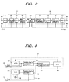
for the reproducing mode by reference to Fig. 2. The
reproduced signal inputted from a terminal 31, after being
converted into a digital signal by the A/D converter 6 and
removed with the low band converted chrominance signal by
a chroma trap 33, is further removed with disturbance due
to inter-modulation and then demodulated into a video signal
through a FM demodulator 35. About the inter-modulation
disturbance will be explained later. The signal processing
up to here is carried out by using the sampling clock (CK3)
of the A/D converter 6 as the clock signal.
An output of the FM demodulator 35 is converted in the
rate into the clock frequency which is used in the video
signal processing with the sampling rate converting circuit
13. In general, since the reproduced signal processing
circuits are mostly designed in common in the circuitry for
the recording signal processing circuits, the signal can
be processed with the same clock frequency as in the
recording mode by doing so, thereby it is possible to
simplify the circuit designing, and in addition thereto,
to achieve small-sizing in the circuit scale.
The video signal which is converted in the sampling
rate thereof is processed into a reproduced signal of
superior S/N ratio with a main de-emphasis circuit 39, a
main LPF 40 for the luminance signal, a non-linear de-emphasis
circuit 41, and a noise canceller 42, and it is
outputted at the terminal 44. The signal is further
processed with a system clock (SYSCK=CK2) which is inputted
from the terminal 45 in the circuitry of downstream from
the sampling rate converting circuit 13.
Next, an explanation will be given on the intermodulation
disturbance mentioned in the above. Here, the
relationship in the frequencies between the reproduced FM
signal and the sampling clock will be explained by referring
to Figs. 4 and 5. Fig. 4 shows the relationship between the
sampling frequency and the frequency allocations under the
standard for 8 mm VTR of NTSC. The FM luminance signal 42
is distributed at the frequency of 4.2 MHz as an edge of
the SYNC and at a frequency of 5.4 MHz as white (100%).
Furthermore, by taking a white clip standard for + 220%
(assuming that to the white (100%) from the edge of the SYNC
is +100%) into a consideration, although not shown in the
drawing, the maximum carrier frequency fwc comes to be at
6.84 MHz. The low band converted chrominance signal 41 is
about at 725 kHz, and it is multiplexed at the lower side
frequency of the FM luminance signal. As shown in Fig. 4,
an upper side-band of the FM luminance signal is lying until
the vicinity of 10 MHz, therefore, the theorem for sampling
cannot be satisfied at the sampling frequency of 4 fsc (14,3
MHz). Further, as the A/D converter, it is assumed that the
converter of 20 MHz at the maximum sampling frequency is
used from a view point of price thereof. Under such the
restriction, as such the sampling clock 43, it is selected
at the frequency 5 fsc (17.9 MHz). Inherently under the 8
mm VTR standard, the FM audio signal is multiplexed at the
frequency between the low band converted chrominance signal
and the FM luminance signal, however, since it has no
relationship with the processing in the video DSP, the
explanation of this is omitted here.
Fig. 5 shows a characteristic of the inter-modulation
disturbance and a low pass filter (hereinafter, it is called
as only a "LPF") for removing it when the sampling is
conducted. In general, when an input signal is converted
from an analogue into a digital with a clock of the sampling
frequency fs, the inter-modulation disturbance will occur
at the frequency difference (fs-f) between the frequency
f of the input signal and the sampling frequency fs. If the
sampling frequency is sufficiently higher than with respect
to that of the input signal, the frequency difference (fs-f)
is also high with respect to that of the input signal, thereby
causing almost no problem. However, in case of A/D
conversion of the FM luminance signal, as indicated with
an arrow 45, since the maximum carrier frequency fwc is high
at 6.87 MHz, the frequency difference (fs-fwc) comes to be
11.06 MHz (as indicated by an arrow of dotted line 46) which
will cause problem when being demodulated with it.
Therefore, with provision of a trap point on an amplitude
characteristic at the frequency of 11.06 MHz with the LPF
which is provided after the A/D conversion, as shown by an
one-dotted chained line 44, the frequency difference
(fs-fwc) is suppressed and the disturbance component of a
broken-line arrow 46 is also fully suppressed as shown by
a solid line arrow 47, thereby removing the disturbance
during the demodulation.
Next, with referring to Fig. 3, a generating method
of the clocks (CK2) and (CK3) will be explained. As shown
in Fig. 2, when convering the sampling rate of the signal,
since the conversion is very difficult if the clock signals
before and after the conversion are not synchronized with
each other, there is a necessity of obtaining the
synchronization between the two clocks previously. The
clock (CK2) is used in the recording mode and in the process
after the sampling rate conversion during the reproducing,
and it is produced with high accuracy by an oscillator 57
by using a crystal oscillator 58 as a reference clock. For
example, the oscillation frequency of the oscillator 57 is
8 fsc. By producing the clock of 4 fsc from a frequency
divider 59, it is outputted as the clock (CK2) at the terminal
52. Further, with respect to the clock (CK3), by oscillating
a desired frequency clock by an oscillator 53, comparing
it in the phase with the output of a frequency divider 59
by a phase comparator 55 after being divided by a frequency
divider 54, and further feeding a phase error through LPF
56 back to a controlled oscillator 53 so as to construct
a PLL loop, it is produced in synchronism with the clock
(CK2) and outputted at a terminal 51. However, blocks 27
and 28 indicated by the frameworks of dotted line are those
corresponding to the PLL circuit 27 and the clock generating
circuit 28, which are shown in Fig. 1.
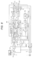
Next, a second embodiment in accordance with the
present invention will be explained by referring to Figs.
6 and 7. Fig. 6 shows the signal processing circuit of the
camcorder. The same elements shown in the embodiment in Fig.
1 are attached with the same reference numerals and the
detailed explanation thereof will be omitted. The
resolution power of the camcorder is determined by the number
of the picture elements or pixels of the image sensor which
is used. In a high grade or quality model is used an image
sensor having a greater number of the picture elements or
pixels, while in an ordinary model an image sensor having
a relative low number of the pixels. Further, when
performing the signal processing in the camera DSP, the
sampling frequency must be different depending on the number
of the pixels. Hereinafter, an explanation will be given
by taking the image sensor as an example which is applied
to the camcorder of the NTSC.
As explained in the embodiment in Fig. 1, those 910
picture elements or pixels are provided for 1H in the image
sensor of high pixel number, and it is the same to the sampling
number when the NTSC signal is sampled with the sampling
frequency 4 fsc. Namely, with the image sensor of high pixel
number, the sampling frequency comes to be 4 fsc. On the
contrary to this, when the number of pixels of the low pixel
number image sensor is selected at 606 or the like for 1H
for example, it is about 2/3 in the number of pixels of the
high pixel image sensor, therefore the sampling frequency
for the low pixel number image sensor is (8/3) fsc. In this
manner, in case of receiving and processing the signal with
the video DSP, the sampling frequency of which must be
different depending on the number of the pixels, since the
circuit which performs the processing is the same in the
structure but is different in the frequency, there is a
necessity of exchanging a coefficient of the circuit in order
to maintain the characteristic at a constant, and this incurs
complicated circuitry designing and increase in gate number
thereof. The number of the pixels of the image sensor is
not always same with manufactures thereof, and is sometimes
different depending on the specification of the set,
therefore it is difficult to determine the circuit constant
readily at a certain value in setting thereof. Taking such
the respects into consideration, in accordance with the
present embodiment, the digital signal transferred from the
camera DSP in the camera recording mode is converted in the
sampling rate, so as to make it equal to the sampling
frequency of the image sensor of high pixel number for a
reference, thereby performing the same processing
thereafter.
Differing from the first embodiment, in the present
embodiment, also for simplifying the explanation thereof,
an A/D converter 102 is so constructed that it is
independently provided with respect to the processing of
the FM signal. As a feature of the system construction, only
one system of an oscillator 109 (here, an oscillator of using
a crystal oscillator 110) is provided for those two (2)
digital processors. Inside of the video DSP 104A, there is
provided a clock generator 107, from which are produced a
system clock (SYSCK) for use in the video DSP 104 and a clock
(REFCK) used as a reference clock of the camera DSP 118.
The camera DSP 118 is also so constructed that it produces
a clock (omitted in Fig. 6) for use inside thereof with a
clock generator 117 on the basis of the REFCK signal
mentioned above, and a clock (EXTCK) in synchronism with
a digital data outputted to the video DSP 104. As mentioned
in the previous embodiment, in case of a sensor of high pixel
number, the above-mentioned EXTCK and the system clock
(SYSCK) in the video DSP 104 can be coincident with each
other in the frequency. For making them coincident with
each other completely, there is one ways in which those two
(2) digital processors are operated on the basis of the same
reference clock, or the other way in which the clock of the
other digital processor is locked in the phase by a PLL
(abbreviation of a "Phase Locked Loop"). The present
embodiment is in accordance with the former method.
Actually, two (2) clocks generated from the same clock are
coincident with each other in the frequency, however, it
is difficult to make them completely coincide with each other
in the phase due to an effect of delay between those two
(2) digital processors, etc. Consequently, when
transferring them between those two (2) digital processors
as they are, it is difficult to take in or fetch the data
with stability. For avoiding this, there are necessitated
sampling rate converting circuits 105 and 106 for converting
a data in synchronism with the clock (EXTCK) outputted from
the camera DSP 118 into a data in synchronism with the system
clock (SYSCK) inside of the video DSP 104.
Fig. 7 shows a construction of the sampling rate
converting circuit. A reference numeral 111 denotes a data
input terminal, 112 an input terminal for the external clock
(EXTCK), 113 a FIFO (abbreviation of First in First out),
115 a system clock input terminal, 114 a sample rate
converting filter, 119 a switching circuit, 120 a control
signal input terminal, and 116 an output terminal. First,
the digital data which is in synchronism with the EXTCK and
inputted from the terminal 111 is converted into a digital
date in synchronism with the SYSCK within the FIFO 113. In
the camcorder using the high pixel number CCD, the output
of the FIFO 113 is transferred through the switching circuit
119 to the output terminal 116, on the while, in the camcorder
using the low pixel number CCD, the output processed by the
FIFO 113, after complementation of the data with the filter
114 for the sampling rate conversion, is outputted through
the switch circuit 119 at the output terminal 116.
In the same manner for either the camcorder with the
low pixel number CCD sensor or the high pixel number CCD
sensor, the outputs of the sampling rate converting circuits
105 and 106 which are obtained in such manner are inputted
to the luminance signal processing circuit 19 and the
chrominance signal processing circuit 20, respectively, and
then, they are converted into the analogue signals with the
D/ A converters 22 and 24 to be recorded onto a magnetic tape
through the recording/reproducing amplifier 2. In this
manner, by conducting the data transfer between those two
(2) digital processors through the sampling rate converting
circuit, in addition of operating those two (2) digital
processors on the basis of the only one oscillator 109,
stable signal transfer can be achieved, and further it can
be converted easily if any one of sensors having various
pixel number is used in the camera portion, thereby obtaining
a merit that the processing thereafter can be unified.
Furthermore, it is explained that the A/D converter 102 is
conditioned of being provided outside of the video DSP, but
alternatively it can be provided inside thereof. Moreover,
the oscillator 109 and the switching circuit 103 are provided
inside of the video DSP 104, but they also may be provided
at the side of the camera DSP without trouble.
Next, a third embodiment in accordance with the
present invention will be explained by referring to Fig.
8. Fig. 8 shows the signal processing circuit of the
camcorder. The same elements shown in the embodiment in Fig.
6 are attached with the same reference numerals and the
detailed explanation thereof will be omitted. The
difference from that shown in Fig. 6 lies in a method for
generating the clock which is used in the camera DSP 124
and video DSP 125. In the present embodiment, an oscillator
127 is provided at the side of the camera DSP 124, and from
the output terminals thereof are outputted the clock (EXTCK)
for use in signal transfer, the clock for use in the A/D
converter 6, and a reference clock (CAMCK) for use as a
reference in the video DSP to the video DSP 125. Within the
video DSP, the above-mentioned reference clock (CAMCK) is
inputted to the PLL circuit 126 to generate a clock in
synchronism with the CAMCK in the phase, and it is sent to
a clock generator 107 so as to produce the system clock
(SYSCK) for use in the video DSP 125, etc. In those sample
rate converting circuit 105 and 106, data transfer is
performed by using the system clock (SYSCK) in synchronism
with the external clock (EXTCK) inputted from the camera
DSP. Operation other than this is the same to that of the
embodiment shown in Fig. 6.
As explained in the above with the second and third
embodiments, the explanation was given basically on the
assumption that those two (2) DSPs are brought in synchronism
with each other by unifying or joining the reference clocks
of the camera DSP and the video DSP as a one signal, however,
if the camera DSP and the video DSP are constructed on the
basis of the clocks which are completely different to each
other, they can be measured by newly-devising the sampling
rate conversion within the breadth of an idea of the present
invention.
Further, in the explanation given in the above, only
the low pixel number sensor and the high pixel number
(standard) sensor are mentioned as the image sensors.
However, there can be considered a camcorder of high quality
picture using another sensor which has the resolution power
higher than that of the high pixel number sensor. In this
case, it is apparent that the signal can be processed in
the same manner as in the process when using the low pixels
number, i.e., by converting into the sampling mode for the
high pixel (standard) mode by using the sampling rate
converting circuit at the side of the video DSP, with respect
to the sampling rate at the side of the camera DSP
corresponding to the high resolution power sensor, within
the breadth of an idea of the present invention.
In accordance with the present invention, by providing
the switching circuit for exchanging among the camera input
signal, the external input signal and the reproduced FM
signal before the A/D converter, as well as selecting the
sampling clock of the A/D converter at the most appropriate
clock with respect to the above-mentioned three (3) signals,
the digital signal processing for both the camera and the
VTR portions can be achieved by only one A/D converter,
thereby bringing great effect in reducing the cost thereof.
Further, by converting the reproduced FM signal into
the first sampling rate by the sampling rate converting
circuit, after converting it from the analogue into the
digital with the second clock which is higher in the
frequency than the first clock for processing the video
signal and is lower than the maximum sampling frequency of
A/D converter which is used, the signal processing after
the conversion can be treated in the same manner as the video
signal processing during the recording operation, thereby
achieving an effect of suppressing complication in the
circuitry designing and of preventing from increase in the
circuit scale, as well as of reducing the cost of the digital
processor.
In particular, by setting the second clock mentioned
above at 5 fsc, it is possible to use such the A/D converter
of lower than 20 MHz in performance, which has been
conventionally used in the camera DSP, thereby achieving
digitalization of the VTR portion without increase in the
cost of the A/D converter thereof.
Further, by suppressing around the frequency
difference (fs-fwc) between the sampling frequency fs and
the maximum carrier frequency fwc after converting the
reproduced FM signal from the analogue into the digital
signal, performance can be sufficiently maintained for the
FM signal processing with the relative low sampling
frequency, such as around 2 times of the FM signal hand.
Further, for the video DSP, by processing with the
clock from the camera DSP when operating in the camera
recording mode and by processing with the clock of the video
DSP when operating in the external input recording mode,
an advantage can be obtained that the signal processings
can be performed with ease for the two (2) signals.
Further, by conducting the data transfer between those
two (2) digital processors through the sampling rate
converting circuit, in addition of operating those two (2)
digital processors (the camera DSP and the video DSP) on
the basis of the only one oscillator, stable signal transfer
can be achieved, and the oscillator can be unified as the
one system, thereby obtaining an effect of reduction in the
cost thereof.
Further, by conducting the conversion from sampling
rate of the low pixel number mode into that of the high
(standard) pixel number mode, and from the sampling rate
of the high accuracy mode into that of the high pixel number
mode with the sampling rate converting circuit so as to make
the frequency at a constant after the conversion for any
mode, the circuits after the sampling rate converting
circuit can be used in common so as to be applied to camcorders
of various specifications, advantageously. Namely, a merit
can be obtained that unification of the circuit boards and
parts can be achieved so as to accomplish reasonable or
rational set designing.
While we have shown and described several embodiments
in accordance with our invention, it should be understood
that disclosed embodiments are susceptible of changes and
modifications without departing from the scope of the
invention. Therefore, we do not intend to be bound by the
details shown and described herein but intend to cover all
such changes and modifications falling within the ambit of
the appended claims.