EP0849785A2 - Method of making a self-aligned contact - Google Patents
Method of making a self-aligned contact Download PDFInfo
- Publication number
- EP0849785A2 EP0849785A2 EP97310455A EP97310455A EP0849785A2 EP 0849785 A2 EP0849785 A2 EP 0849785A2 EP 97310455 A EP97310455 A EP 97310455A EP 97310455 A EP97310455 A EP 97310455A EP 0849785 A2 EP0849785 A2 EP 0849785A2
- Authority
- EP
- European Patent Office
- Prior art keywords
- forming
- silicon
- nitride
- rich
- layer
- Prior art date
- Legal status (The legal status is an assumption and is not a legal conclusion. Google has not performed a legal analysis and makes no representation as to the accuracy of the status listed.)
- Withdrawn
Links
Images

Classifications
-
- H—ELECTRICITY
- H01—ELECTRIC ELEMENTS
- H01L—SEMICONDUCTOR DEVICES NOT COVERED BY CLASS H10
- H01L21/00—Processes or apparatus adapted for the manufacture or treatment of semiconductor or solid state devices or of parts thereof
- H01L21/70—Manufacture or treatment of devices consisting of a plurality of solid state components formed in or on a common substrate or of parts thereof; Manufacture of integrated circuit devices or of parts thereof
- H01L21/71—Manufacture of specific parts of devices defined in group H01L21/70
- H01L21/768—Applying interconnections to be used for carrying current between separate components within a device comprising conductors and dielectrics
- H01L21/76897—Formation of self-aligned vias or contact plugs, i.e. involving a lithographically uncritical step
-
- H—ELECTRICITY
- H01—ELECTRIC ELEMENTS
- H01L—SEMICONDUCTOR DEVICES NOT COVERED BY CLASS H10
- H01L23/00—Details of semiconductor or other solid state devices
- H01L23/28—Encapsulations, e.g. encapsulating layers, coatings, e.g. for protection
- H01L23/31—Encapsulations, e.g. encapsulating layers, coatings, e.g. for protection characterised by the arrangement or shape
- H01L23/3157—Partial encapsulation or coating
- H01L23/3171—Partial encapsulation or coating the coating being directly applied to the semiconductor body, e.g. passivation layer
-
- H—ELECTRICITY
- H01—ELECTRIC ELEMENTS
- H01L—SEMICONDUCTOR DEVICES NOT COVERED BY CLASS H10
- H01L23/00—Details of semiconductor or other solid state devices
- H01L23/48—Arrangements for conducting electric current to or from the solid state body in operation, e.g. leads, terminal arrangements ; Selection of materials therefor
- H01L23/482—Arrangements for conducting electric current to or from the solid state body in operation, e.g. leads, terminal arrangements ; Selection of materials therefor consisting of lead-in layers inseparably applied to the semiconductor body
- H01L23/485—Arrangements for conducting electric current to or from the solid state body in operation, e.g. leads, terminal arrangements ; Selection of materials therefor consisting of lead-in layers inseparably applied to the semiconductor body consisting of layered constructions comprising conductive layers and insulating layers, e.g. planar contacts
-
- H—ELECTRICITY
- H01—ELECTRIC ELEMENTS
- H01L—SEMICONDUCTOR DEVICES NOT COVERED BY CLASS H10
- H01L2924/00—Indexing scheme for arrangements or methods for connecting or disconnecting semiconductor or solid-state bodies as covered by H01L24/00
- H01L2924/0001—Technical content checked by a classifier
- H01L2924/0002—Not covered by any one of groups H01L24/00, H01L24/00 and H01L2224/00
-
- H—ELECTRICITY
- H01—ELECTRIC ELEMENTS
- H01L—SEMICONDUCTOR DEVICES NOT COVERED BY CLASS H10
- H01L2924/00—Indexing scheme for arrangements or methods for connecting or disconnecting semiconductor or solid-state bodies as covered by H01L24/00
- H01L2924/10—Details of semiconductor or other solid state devices to be connected
- H01L2924/11—Device type
- H01L2924/12—Passive devices, e.g. 2 terminal devices
- H01L2924/1204—Optical Diode
- H01L2924/12044—OLED
-
- H—ELECTRICITY
- H01—ELECTRIC ELEMENTS
- H01L—SEMICONDUCTOR DEVICES NOT COVERED BY CLASS H10
- H01L2924/00—Indexing scheme for arrangements or methods for connecting or disconnecting semiconductor or solid-state bodies as covered by H01L24/00
- H01L2924/19—Details of hybrid assemblies other than the semiconductor or other solid state devices to be connected
- H01L2924/1901—Structure
- H01L2924/1904—Component type
- H01L2924/19041—Component type being a capacitor
-
- Y—GENERAL TAGGING OF NEW TECHNOLOGICAL DEVELOPMENTS; GENERAL TAGGING OF CROSS-SECTIONAL TECHNOLOGIES SPANNING OVER SEVERAL SECTIONS OF THE IPC; TECHNICAL SUBJECTS COVERED BY FORMER USPC CROSS-REFERENCE ART COLLECTIONS [XRACs] AND DIGESTS
- Y10—TECHNICAL SUBJECTS COVERED BY FORMER USPC
- Y10S—TECHNICAL SUBJECTS COVERED BY FORMER USPC CROSS-REFERENCE ART COLLECTIONS [XRACs] AND DIGESTS
- Y10S257/00—Active solid-state devices, e.g. transistors, solid-state diodes
- Y10S257/90—MOSFET type gate sidewall insulating spacer
Definitions
- This invention relates in general to the field of semiconductor devices, and more specifically to a method for enhancing the performance of a contact in a semiconductor device.
- Semiconductor device fabrication involves the formation of different components on a substrate using a variety of techniques, such as deposition, patterning, and etching.
- One component in semiconductor devices is a contact for coupling a layer of material to the underlying substrate or another layer.
- contacts may be holes, vias, channels, or other geometric structures.
- One type of contact is a self-aligned contact. Self-aligned contacts are commonly used to decrease cell areas, which provides increased packing density.
- Etches for self-aligned contacts differ from etches for standard contacts because of the presence of an exposed shoulder of, for example, nitride, in the self-aligned contact structure that is very susceptible to etch erosion. Such a shoulder is not present in standard contacts. Because the exposed shoulder is susceptible to etch erosion, the etchant should etch the material on the exposed shoulder at a much slower rate than it etches the material in the proximity of the shoulder. For a given design, higher etch selectivities may increase the contact area. The greater the contact area, the lower the sheet resistance and the better the performance of the semiconductor device. Additionally, higher etch selectivities contribute to preventing electrical shorts near the shoulder.
- One method for effecting a high etch selectivity is modifying the chemistry of the etchant.
- adjusting the chemistry of the etchant may lead to the detrimental problem of stop-etch, which is generally an incomplete etch due to polymer build-up.
- Another method for effecting a high etch selectivity is adjusting the etch process parameters, such as temperature. Adjusting such parameters is commonly referred to as "knob" changes.
- knock changes may not always be accomplished in a timely fashion and therefore may be inadequate to effectively increase selectivity.
- a method for forming a contact to a substrate of a semiconductor device includes forming a stopping layer overlying the substrate, the stopping layer comprising a material selected from the group consisting of silicon-rich nitride, silicon-rich oxide, carbon-rich nitride, silicon carbide, boron nitride, organic spin-on-glass, graphite, diamond, carbon-rich oxide, nitrided oxide, and organic polymer.
- the method further includes forming an insulating layer overlying the stopping layer and etching portions of the insulating layer to define a contact region. The method also includes removing portions of the stopping layer in the contact region.
- a semiconductor device formed in a surface of a substrate and having a gate and a self-aligned contact includes a first conductive material forming a portion of the gate and a second conductive material forming a portion of the self-aligned contact, the conductive material contacting the substrate.
- the semiconductor device further comprises a dielectric material structure contacting both the first conductive material and the second conductive material, the dielectric material selected from the group consisting of silicon-rich nitride, silicon-rich oxide, carbon-rich nitride, silicon carbide, boron nitride, organic spin-on-glass, graphite, diamond, carbon-rich oxide, nitrided oxide, and organic polymer.
- Important technical advantages of the invention include providing a method for increasing the selectivity with respect to an etch in a self-aligned contact structure. Therefore, the invention provides a method for forming a self-aligned contact with a reduced possibility of a short near the shoulder of a self-aligned contact. Furthermore, the invention allows for maximizing the area on the substrate that is in contact with a self-aligned contact. The large contact area reduces the contact resistance and therefore increases the performance of the semiconductor device.
- etch selectivity without necessarily adjusting the chemistry of the etchant. Therefore, problems previously associated with such a procedure, such as stop etch, may be avoided. Furthermore, greater etch selectivity may be achieved without requiring "knob" changes, which may be ineffective or may adversely affect other portions of the manufacture of the semiconductor device.
- FIGURES 1A through 3 of the drawings like numerals being used for like and corresponding parts of the various drawings.
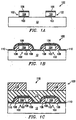
- FIGURES 1A through 1F illustrate a method for forming a self-aligned contact to substrate 12.
- FIGURE 1A illustrates a cross section of semiconductor device 100 during fabrication, which already includes gates 102 formed overlying substrate 12.
- Substrate 12 comprises silicon, silicon on insulator (SOI), or any other appropriate substrate for semiconductor fabrication.
- Substrate 12 may comprise a layer of material formed over a substrate of a semiconductor device.
- gates 102 comprise a gate dielectric film 103, a conductive film 104 overlying gate dielectric film 103, and an insulating film 106 overlying conductive film 104.
- Gates 102 may be formed using any suitable technique, for example by: depositing or thermally growing gate dielectric film 103; depositing conductive film 104 overlying gate dielectric film 103; depositing insulating film 106 overlying conductive film 104; and patterning gate dielectric film 103, conductive film 104, and insulating film 106 together to form gates 102.
- Gate dielectric film 103 may be formed from oxide, oxynitride, or other suitable material with the desired dielectric properties.
- Conductive film 104 may be a metal, amorphous polysilicon, polysilicides, tungsten silicides, or other appropriate conductive material, as well as any combination of these films.
- insulating film 106 may be formed from nitride with or without some oxide, or from other suitable insulating film or film combinations.
- insulating film 106 may comprise a material selected to increase the selectivity of an etch with respect to insulating film 106 and therefore reduce the possibility of a short between the gate conductive film 104 and a subsequently formed contact.
- Forming insulating film 106 from materials that increase the selectivity of an etch with respect to insulating material 106 allows for increased contact area for the self-aligned contact, enhancing the performance of semiconductor device 100. Suitable materials for insulating material 106 are discussed in greater detail below.
- FIGURE 1B illustrates device 100 after forming insulating sidewalls 108 overlying gates 102 with a stopping layer 110.
- sidewalls 108 may be formed by depositing an insulating material, such as oxide or nitride, using a low pressure or plasma chemical vapor deposition (CVD) technique; however other deposition techniques may be used. The insulating material is then anisotropically etched until a desired portion of substrate 12 between gates 102 is exposed.
- sidewalls 108 may comprise a material that provides increased selectivity for an etch process with respect to the sidewall 108.
- Stopping layer 110 may be formed, for example, by depositing a layer of appropriate dielectric material overlying gates 102 and insulating sidewalls 108 using a CVD technique. Alternative suitable deposition or growth techniques may also be used to form stopping layer 110. An appropriate material used to form stopping layer 110 is discussed in greater detail below in conjunction with FIGURE 1D.
- FIGURE 1C illustrates device 100 after several additional process steps, including: forming insulating layer 112 overlying stopping layer 110, forming mask 116 overlying insulating layer 112, and patterning mask 116 to define contact region 118.
- Insulating layer 112 may be formed using any appropriate deposition or growth technique, including without limitation chemical deposition at low pressure or using plasma, spin coating, sputtering, or other deposition or growth techniques.
- Insulating layer 112 may comprise oxide or a doped oxide, such as for example, boron phospho-silicate glass (BPSG) or other suitable material for electrically insulating components in semiconductor device 110.
- BPSG boron phospho-silicate glass
- Mask 116 may comprise any suitable patterning material that can define contact region 118.
- mask 116 may be a negative or positive photoresist that is patterned using an appropriate photolithography technique.
- a planarization technique may be included during any phase of the formation of device 100 illustrated in FIGURE 1C. For example, after forming insulating layer 112, a planarization technique may be employed before forming mask 116. Planarization may be accomplished by a reflow process, spin coating, chemical or mechanical polishing, a planarization etch, or other appropriate planarization technique.
- FIGURE 1D illustrates device 100 after removing portions of insulating layer 112 in contact region 118.
- the removal process may be performed by, for example, an anisotropic etch that is selective to stopping layer 110.
- Example etchants comprise compounds comprising carbon and fluorine; however, other etchants may be used.
- insulating layer 112 may be removed with a C 4 F 8 etchant.
- etching if the etch is not selective enough with respect to stopping layer 110, stopping layer 110 is susceptible to erosion, which is undesirable. Erosion in shoulder region 113 may be particularly deleterious to semiconductor device 110 because a short may develop between conductive material 104 and a subsequently formed self-aligned contact 122, shown in FIGURE 1F.
- stopping layer 110 is formed from an appropriate material that increases the selectivity of the etch with respect to stopping layer 110. Materials appropriate for use as stopping layer 110 are discussed in greater detail below.
- the stopping layer 110 may be removed by a second anisotropic etch selective to sidewall region 108 and insulating film 106, resulting in the structure illustrated in FIGURE 1E.
- the resulting structure comprises contact region 118 defined by the removal of vertically aligned portions of stopping layer 110 and insulating layer 112.
- Stopping layer 110 is formed from an appropriate material that may result in an etch that is more selective to stopping insulating layer 110 than to conventional masking materials, such as nitride. If the etch selectivity between insulating layer 112 and stopping layer 110 is not great enough, stopping layer 110 may significantly erode during etching of insulating layer 112. If such erosion occurs, the subsequent etch of stopping layer 110 to expose substrate 12, as illustrated in FIGURE 1E, requires a higher degree of selectivity with respect to insulating film 106 and sidewall 108 than would be required if stopping layer 110 experienced no erosion during etching of insulating layer 112. Alternately, insulating film 106 and sidewall 108 could be formed with a greater thickness to compensate for such erosion.
- an appropriate material for stopping layer 110 may allow the use of thinner films for insulating film 106 and sidewall 108, which increases contact area and improves planarity.
- the use of an appropriate material for stopping layer 110 may allow the insulating film 106 and sidewall 108 to be chosen based on their dielectric properties rather than for their etch selectivity.
- an electrical short between the conductive film 104 and subsequently formed contact 122, illustrated in FIGURE 1F may occur. Such a short is most likely to occur near shoulder region 113, illustrated in FIGURE 1D.
- an etch may be terminated prematurely, leaving a portion of stopping layer 110 overlying substrate 12 and therefore reducing the contact area. Reduction of contact area may be detrimental to the performance of semiconductor device 100. Therefore, increasing the selectivity of an etch with respect to stopping layer is desirable.
- stopping layer 110 should be formed from an appropriate material.
- One such material comprises silicon-rich nitride. Silicon-rich nitride possesses more silicon than stoichiometric nitride.
- stopping layer 110 comprises silicon-rich nitride having a silicon to nitrogen ratio greater than 0.75:1. In another embodiment, silicon to nitrogen ratios of approximately 1.5:1 to 2.0:1 may be particularly advantageous. However, any silicon level greater than that required by stoichiometric proportions may be used.
- the extra silicon in stopping layer 110 affects the chemical reactions associated with the use of common etchants used with nitride, such as C 4 F 8 , making the etchant more selective to stopping layer 110 than it is without the extra silicon in stopping layer 110.
- Other materials that affect the chemical reactions that occur with various etchants that may be used to etch insulting layer 112 and that may be used in stopping layer 110 comprise carbon-rich nitride, silicon-rich oxide, organic spin-on-glass, silicon carbide, carbon-rich oxide, nitrided oxide, and organic polymers.
- carbon-rich nitride designates nitride possessing some carbon
- carbon-rich oxide designates oxide possessing some carbon.
- silicon carbide for use within or as a stopping layer 110 provides a physically harder stopping layer 110 to etch. Therefore, in addition to gains in selectivity attained through chemistry, silicon carbide also affects the mechanical portion of an etch and therefore increases selectivity with respect to stopping layer 110.
- Other materials that may be used for stopping layer 110 that increase selectivity due to increased hardness comprise carbon-rich nitride, graphite, diamond, nitrided oxide, and boron nitride.
- FIGURE 1F illustrates device 100 after forming conductive material 120 in contact region 118 to complete fabrication of self-aligned contact, shown generally as element 122. Due to the etch selectivity of first stopping layer 110 the surface area of the contact between the self-aligned contact 122 and the substrate 12 may be maximized. Furthermore, the possibility of a short occurring near shoulder 113 illustrated in FIGURE 1B is reduced by the increased selectivity of the etch to layer 110. Self-aligned contact 122 couples substrate 12 and one or more overlying layers using the limited space between gates 102. Further fabrication of device 100 may incorporate contact 122 into a storage node capacitor, transistor, bit line component, word line component, or any other suitable component in a semiconductor device.
- a stopping layer 110 comprising one of the above materials may be deposited as discussed above in conjunction with FIGURE 1B.
- a standard dielectric such as nitride
- nitride may be deposited and then implanted with appropriate implants to provide the desired above-mentioned physical or chemical properties for stopping layer 110.
- Appropriate implants for nitride comprise silicon, boron, and carbon.
- an appropriate level of implantation of silicon comprises silicon-rich nitride having a7 silicon to nitrogen ratio greater than 0.75:1.
- silicon to nitrogen ratios of approximately 1.5:1 to 2.0:1 may be particularly advantageous.
- any suitable level of implantation that increases the selectivity of the etchant with respect to the stopping layer 110 may be used.
- a hexamethyldisiloxane (HMDS) treatment may be applied to nitride with the result of increasing the silicon level of the nitride.
- HMDS hexamethyldisiloxane
- Other surface treatments that increase the level of a desired element in materials used to form stopping layer 110 may also be used.
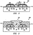
- FIGURE 2 illustrates one method for implanting suitable materials to form stopping layer 110.
- suitable materials are implanted into stopping layer 110 at an angle approximately 45 degrees from the horizontal.
- the angle of implantation measured from a plane parallel to the substrate, is chosen so that the implants will collide in a perpendicular fashion with stopping layer 110 at portions of the stopping layer where etch selectivity is most important.
- the angle of implantation selected may be dependent upon the geometry of shoulder region 113. Because the region of stopping layer 110 that is perpendicular to the angle of implantation receives more of the implant material, stopping layer 110 will have a higher concentration of implant in the region of stopping layer 110 perpendicular to the angle of implantation.
- the selectivity of the etch to the shoulder region 113 may be selectively increased.
- the increased levels of suitable materials implanted may be concentrated in areas where the selectivity effects are most greatly needed without increasing levels of implanted material unnecessarily in regions of stopping layer 110 where increased selectivity is not as critical. Therefore, any deleterious effects on the manufacturing process that may be attributable to increased levels of implanted material may be minimized.
- conventional implantation techniques may also be used to form the desired material for stopping layer 110.
- FIGURE 3 illustrates a completed self-aligned contact.
- the formation of the device 200 illustrated in FIGURE 3 is substantially similar to the formation of device 100. However, stopping layer 110 is not used. Because stopping layer 110 is not used, only one etch is required to expose the surface of substrate 12 underlying insulating layer 112.
- sidewall 108 and insulating film 106 may be formed from the materials discussed above in conjunction with the formation of layer 110.
- the formation of sidewall 108 and thin film 106 may also comprise implantation or surface treatment in a similar manner to that discussed above in conjunction with FIGURES 1A through 1F and FIGURE 2.
- Forming insulating film 106 and sidewall 108 from materials that provide increased etch selectively with respect to insulating film 106 and sidewall 108 decreases the possibility of a short between conductive film 104 and self-aligned contact 122 and additionally maximizes the surface area of the contact between substrate 12 and self-aligned contact 120, which enhances the performance of device 200.
- forming insulating film 106 and sidewall 108 from materials that provide increased etch selectivity with respect to insulating film 106 and side wall 108 decreases the possibility of premature termination of an etch because insulating layer 112 may be completely etched without significantly eroding insulating film 106 or sidewall 108. Therefore, the contact area between substrate 12 and self-aligned contact 122 may be maximized.
Abstract
Description
Claims (21)
- A method for forming a contact, comprising:forming a stopping layer overlying a substrate;forming an insulating layer overlying the stopping layer;etching portions of the insulating layer to define a contact region; andremoving portions of the stopping layer in the contact region.
- The method of Claim 1, wherein the step of forming the stopping layer comprises forming the stopping layer from a material selected from a group of materials comprising: silicon-rich nitride, silicon-rich oxide, carbon-rich nitride, carbon-rich oxide, silicon carbine, boron nitride, organic spin-on-glass, graphite, diamond, nitrided oxide and organic polymer.
- The method of Claim 1 or Claim 2, wherein the step of forming the stopping layer comprises forming the stopping layer from silicon-rich nitride having a silicon to nitrogen ratio in the range of approximately 1.5:1 to 2.0:1.
- The method of any of Claims 1 to 3, wherein the step of forming the stopping layer comprises the steps of:forming a nitride layer; andimplanting into the nitride layer an implant material
- The method of Claim 4, wherein the step of implanting the implant material into the nitride layer comprises implanting an implant material selected from a group of materials comprising: silicon, carbon and boron.
- The method of Claim 4 or 5, wherein the step of implanting into the nitride layer comprises implanting the material at a selected angle to provide a higher concentration of implanted material at a desired portion of the nitride layer than at other portions of the nitride layer.
- The method of Claim 6, wherein the step of implanting the implant material into the nitride layer comprises implanting the implant material at a selected angle of approximately forty-five degrees.
- The method of any of Claims 1 to 3, wherein the step of forming the stopping layer comprises the steps of:forming a nitride layer; andtreating portions of the nitride layer with hexamethyldisilazene to increase silicon content in the nitride layer.
- The method of any of Claims 1 to 8, wherein the step of etching portions of the insulating layer comprises the step of etching portions of the insulating layer with an etchant comprising carbon and fluorine.
- A method for forming a self-aligned contact to a substrate proximate a gate of a field-effect transistor, comprising:forming a first film overlying the substrate;forming a conductive film overlying the first film to form a conductive portion of the gate;forming a second film overlying the conductive film;forming a sidewall associated with the conductive film;forming an insulating layer overlying the second film and overlying the sidewall; andremoving portions of the insulating layer to define a contact region.
- The method of Claim 10, wherein the step of forming the second film comprises forming the second film from a material selected from a group of material comprising: silicon-rich nitride, silicon-rich oxide, carbon-rich nitride, carbon-rich oxide, silicon carbide, boron nitride, organic spin-on-glass, graphite, diamond, nitrided oxide and organic polymer.
- The method of Claim 10 or Claim 11, wherein the step of forming the sidewall comprises forming the sidewall selected from a group of materials comprising: silicon-rich nitride, silicon-rich oxide, carbon-rich nitride, silicon carbide, boron nitride, organic spin-on- and organic polymer, and combinations thereof.
- The method of any of Claims 10 to 12, wherein the step of forming the second film comprises forming the second film from silicon-rich nitride having a silicon to nitrogen ratio in the range of approximately 1.5:1 to 2.0:1.
- The method of any of Claims 10 to 13, wherein the step of forming a second film comprises the steps of:forming a nitride layer overlying the conductive film; andimplanting into the nitride layer an implant material.
- The method of Claim 14, wherein the step of implanting the implant material into the nitride layer comprises implanting an implant material selected from a group of materials comprising: silicon, carbon and boron.
- The method of any of Claims 10 to 14, wherein the step of forming the sidewall comprises forming the sidewall from silicon-rich nitride having a silicon to nitrogen ratio in the range of approximately 1.5:1 to 2.0:1.
- A semiconductor device formed in a substrate and having a gate and a self-aligned contact, the semiconductor device comprising:a first conductive material forming a portion of the gate;a second conductive material forming a portion of the self-aligned contact, the second conductive material contacting the substrate; anda dielectric material structure contacting both the first conductive material and the second conductive material.
- The semiconductor device of Claim 17, wherein the dielectric material is selected from a group of materials comprising: silicon-rich nitride, silicon-rich oxide, carbon-rich nitride, carbon-rich oxide, silicon carbide, boron nitride, organic spin-on-glass, graphite, diamond, nitrided oxide and organic polymer.
- The semiconductor device of Claim 17 or Claim 18, wherein the dielectric material structure, comprises a sidewall spacer adjacent the conductive film.
- The semiconductor device of any of Claims 17 to 19, wherein the dielectric material structure overlies the conductive film.
- The semiconductor device of any of Claims 17 to 20, wherein the dielectric material comprises silicon-rich nitride having a silicon to nitrogen ratio in the range of approximately 1.5:1 to 2.0:1.
Applications Claiming Priority (2)
| Application Number | Priority Date | Filing Date | Title |
|---|---|---|---|
| US3313496P | 1996-12-20 | 1996-12-20 | |
| US33134P | 1996-12-20 |
Publications (2)
| Publication Number | Publication Date |
|---|---|
| EP0849785A2 true EP0849785A2 (en) | 1998-06-24 |
| EP0849785A3 EP0849785A3 (en) | 1998-12-30 |
Family
ID=21868736
Family Applications (1)
| Application Number | Title | Priority Date | Filing Date |
|---|---|---|---|
| EP97310455A Withdrawn EP0849785A3 (en) | 1996-12-20 | 1997-12-22 | Method of making a self-aligned contact |
Country Status (3)
| Country | Link |
|---|---|
| US (1) | US6136700A (en) |
| EP (1) | EP0849785A3 (en) |
| JP (1) | JPH10189736A (en) |
Cited By (10)
| Publication number | Priority date | Publication date | Assignee | Title |
|---|---|---|---|---|
| EP0908941A2 (en) * | 1997-09-29 | 1999-04-14 | Siemens Aktiengesellschaft | Deposition of carbon into nitride layer for improved selectivity of oxide to nitride etchrate for self aligned contact etching |
| GB2338596A (en) * | 1998-06-17 | 1999-12-22 | Samsung Electronics Co Ltd | Method for forming a self aligned contact in a semiconductor device |
| GB2357186A (en) * | 1999-08-27 | 2001-06-13 | Lucent Technologies Inc | Self-aligned contact process involving forming an opening in carbide or nitride layer over a gate |
| EP1152460A2 (en) * | 2000-04-25 | 2001-11-07 | Infineon Technologies North America Corp. | Method of etching a contact by RIE using a low temperature carbon rich oxy-nitride layer for improving etching selectivity |
| KR100346449B1 (en) * | 1999-07-24 | 2002-07-27 | 주식회사 하이닉스반도체 | Manufacturing method for semiconductor device |
| EP1267397A1 (en) * | 2001-06-11 | 2002-12-18 | Infineon Technologies SC300 GmbH & Co. KG | Semiconductor device with self-aligned contact and method for manufacturing said device |
| EP1498939A3 (en) * | 2003-01-24 | 2006-01-04 | Texas Instruments Incorporated | Method of forming integrated circuit contacts |
| US7208423B2 (en) * | 2001-03-29 | 2007-04-24 | Kabushiki Kaisha Toshiba | Semiconductor device fabrication method and semiconductor device |
| US8106383B2 (en) | 2009-11-13 | 2012-01-31 | International Business Machines Corporation | Self-aligned graphene transistor |
| US8158527B2 (en) | 2001-04-20 | 2012-04-17 | Kabushiki Kaisha Toshiba | Semiconductor device fabrication method using multiple resist patterns |
Families Citing this family (18)
| Publication number | Priority date | Publication date | Assignee | Title |
|---|---|---|---|---|
| US6274479B1 (en) * | 1998-08-21 | 2001-08-14 | Micron Technology, Inc | Flowable germanium doped silicate glass for use as a spacer oxide |
| US6974766B1 (en) * | 1998-10-01 | 2005-12-13 | Applied Materials, Inc. | In situ deposition of a low κ dielectric layer, barrier layer, etch stop, and anti-reflective coating for damascene application |
| US6251802B1 (en) * | 1998-10-19 | 2001-06-26 | Micron Technology, Inc. | Methods of forming carbon-containing layers |
| KR100430690B1 (en) * | 1998-12-30 | 2004-07-27 | 주식회사 하이닉스반도체 | Contact Forming Method of Semiconductor Device |
| US6258714B1 (en) * | 1999-04-01 | 2001-07-10 | Alliance Semiconductor Corporation | Self-aligned contacts for salicided MOS devices |
| KR100324933B1 (en) * | 1999-06-21 | 2002-02-28 | 박종섭 | method for forming self-align contact hole in semiconductor device |
| US6573565B2 (en) * | 1999-07-28 | 2003-06-03 | International Business Machines Corporation | Method and structure for providing improved thermal conduction for silicon semiconductor devices |
| JP3430091B2 (en) | 1999-12-01 | 2003-07-28 | Necエレクトロニクス株式会社 | Etching mask, method of forming contact hole using etching mask, and semiconductor device formed by the method |
| KR100431822B1 (en) * | 1999-12-28 | 2004-05-20 | 주식회사 하이닉스반도체 | Method for forming contact in semiconductor device |
| KR100339683B1 (en) * | 2000-02-03 | 2002-06-05 | 윤종용 | Method of forming self-aligned contact structure in semiconductor integrated circuit device |
| KR100379531B1 (en) * | 2000-12-29 | 2003-04-10 | 주식회사 하이닉스반도체 | method for manufacturing of semiconductor device |
| US6784098B1 (en) * | 2001-04-30 | 2004-08-31 | Taiwan Semiconductor Manufacturing Company | Method for forming salicide process |
| US6764929B1 (en) * | 2002-05-16 | 2004-07-20 | Advanced Micro Devices, Inc. | Method and system for providing a contact hole in a semiconductor device |
| US6861751B2 (en) * | 2002-12-09 | 2005-03-01 | Integrated Device Technology, Inc. | Etch stop layer for use in a self-aligned contact etch |
| KR100645458B1 (en) * | 2003-10-02 | 2006-11-13 | 주식회사 하이닉스반도체 | Method for fabrication of semiconductor device capable of protecting attack by wet cleaning |
| CN101866850B (en) * | 2009-04-14 | 2014-10-22 | 中芯国际集成电路制造(北京)有限公司 | Structure of salicide area barrier film and preparation method thereof |
| US8772102B2 (en) * | 2012-04-25 | 2014-07-08 | Globalfoundries Inc. | Methods of forming self-aligned contacts for a semiconductor device formed using replacement gate techniques |
| US8741723B2 (en) * | 2012-04-25 | 2014-06-03 | Globalfoundries Inc. | Methods of forming self-aligned contacts for a semiconductor device |
Citations (5)
| Publication number | Priority date | Publication date | Assignee | Title |
|---|---|---|---|---|
| US5166096A (en) * | 1991-10-29 | 1992-11-24 | International Business Machines Corporation | Process for fabricating self-aligned contact studs for semiconductor structures |
| US5286667A (en) * | 1992-08-11 | 1994-02-15 | Taiwan Semiconductor Manufacturing Company | Modified and robust self-aligning contact process |
| EP0680084A1 (en) * | 1994-04-28 | 1995-11-02 | Texas Instruments Incorporated | Self-aligned via using low permittivity dielectric |
| US5578524A (en) * | 1994-03-30 | 1996-11-26 | Nec Corporation | Fabrication process of a semiconductor device with a wiring structure |
| EP0746017A2 (en) * | 1995-05-29 | 1996-12-04 | Sony Corporation | Method of forming connection hole |
Family Cites Families (7)
| Publication number | Priority date | Publication date | Assignee | Title |
|---|---|---|---|---|
| EP0014689A1 (en) * | 1979-02-13 | 1980-08-20 | Ciba-Geigy Ag | Auxiliary agent and its use in the dyeing or optical bleaching of polyester textile materials |
| US4364165A (en) * | 1981-05-28 | 1982-12-21 | General Motors Corporation | Late programming using a silicon nitride interlayer |
| JPS6010644A (en) * | 1983-06-30 | 1985-01-19 | Toshiba Corp | Semiconductor device and manufacture thereof |
| US5691246A (en) * | 1993-05-13 | 1997-11-25 | Micron Technology, Inc. | In situ etch process for insulating and conductive materials |
| US5510281A (en) * | 1995-03-20 | 1996-04-23 | General Electric Company | Method of fabricating a self-aligned DMOS transistor device using SiC and spacers |
| US5622596A (en) * | 1995-05-08 | 1997-04-22 | International Business Machines Corporation | High density selective SiO2 :Si3 N4 etching using a stoichiometrically altered nitride etch stop |
| US5897372A (en) * | 1995-11-01 | 1999-04-27 | Micron Technology, Inc. | Formation of a self-aligned integrated circuit structure using silicon-rich nitride as a protective layer |
-
1997
- 1997-12-17 US US08/992,268 patent/US6136700A/en not_active Expired - Lifetime
- 1997-12-22 JP JP9370141A patent/JPH10189736A/en active Pending
- 1997-12-22 EP EP97310455A patent/EP0849785A3/en not_active Withdrawn
Patent Citations (5)
| Publication number | Priority date | Publication date | Assignee | Title |
|---|---|---|---|---|
| US5166096A (en) * | 1991-10-29 | 1992-11-24 | International Business Machines Corporation | Process for fabricating self-aligned contact studs for semiconductor structures |
| US5286667A (en) * | 1992-08-11 | 1994-02-15 | Taiwan Semiconductor Manufacturing Company | Modified and robust self-aligning contact process |
| US5578524A (en) * | 1994-03-30 | 1996-11-26 | Nec Corporation | Fabrication process of a semiconductor device with a wiring structure |
| EP0680084A1 (en) * | 1994-04-28 | 1995-11-02 | Texas Instruments Incorporated | Self-aligned via using low permittivity dielectric |
| EP0746017A2 (en) * | 1995-05-29 | 1996-12-04 | Sony Corporation | Method of forming connection hole |
Cited By (18)
| Publication number | Priority date | Publication date | Assignee | Title |
|---|---|---|---|---|
| EP0908941A3 (en) * | 1997-09-29 | 2004-02-11 | Siemens Aktiengesellschaft | Deposition of carbon into nitride layer for improved selectivity of oxide to nitride etchrate for self aligned contact etching |
| EP0908941A2 (en) * | 1997-09-29 | 1999-04-14 | Siemens Aktiengesellschaft | Deposition of carbon into nitride layer for improved selectivity of oxide to nitride etchrate for self aligned contact etching |
| GB2338596A (en) * | 1998-06-17 | 1999-12-22 | Samsung Electronics Co Ltd | Method for forming a self aligned contact in a semiconductor device |
| GB2338596B (en) * | 1998-06-17 | 2001-08-15 | Samsung Electronics Co Ltd | Process for use in forming a self aligned contact in a semiconductor device |
| KR100346449B1 (en) * | 1999-07-24 | 2002-07-27 | 주식회사 하이닉스반도체 | Manufacturing method for semiconductor device |
| GB2357186A (en) * | 1999-08-27 | 2001-06-13 | Lucent Technologies Inc | Self-aligned contact process involving forming an opening in carbide or nitride layer over a gate |
| EP1152460A3 (en) * | 2000-04-25 | 2004-02-25 | Infineon Technologies North America Corp. | Method of etching a contact by RIE using a low temperature carbon rich oxy-nitride layer for improving etching selectivity |
| EP1152460A2 (en) * | 2000-04-25 | 2001-11-07 | Infineon Technologies North America Corp. | Method of etching a contact by RIE using a low temperature carbon rich oxy-nitride layer for improving etching selectivity |
| US7208423B2 (en) * | 2001-03-29 | 2007-04-24 | Kabushiki Kaisha Toshiba | Semiconductor device fabrication method and semiconductor device |
| US7824996B2 (en) | 2001-03-29 | 2010-11-02 | Kabushiki Kaisha Toshiba | Semiconductor device fabrication method and semiconductor device |
| US8163611B2 (en) | 2001-03-29 | 2012-04-24 | Kabushiki Kaisha Toshiba | Semiconductor device fabrication method and semiconductor device |
| US8183119B2 (en) | 2001-03-29 | 2012-05-22 | Kabushiki Kaisha Toshiba | Semiconductor device fabrication method using multiple mask patterns |
| US8158527B2 (en) | 2001-04-20 | 2012-04-17 | Kabushiki Kaisha Toshiba | Semiconductor device fabrication method using multiple resist patterns |
| EP1267397A1 (en) * | 2001-06-11 | 2002-12-18 | Infineon Technologies SC300 GmbH & Co. KG | Semiconductor device with self-aligned contact and method for manufacturing said device |
| US6784553B2 (en) | 2001-06-11 | 2004-08-31 | Infineon Technologies Sc300 Gmbh & Co. Kg | Semiconductor device with self-aligned contact and method for manufacturing the device |
| EP1498939A3 (en) * | 2003-01-24 | 2006-01-04 | Texas Instruments Incorporated | Method of forming integrated circuit contacts |
| US7087479B2 (en) | 2003-01-24 | 2006-08-08 | Texas Instruments Incorporated | Method of forming integrated circuit contacts |
| US8106383B2 (en) | 2009-11-13 | 2012-01-31 | International Business Machines Corporation | Self-aligned graphene transistor |
Also Published As
| Publication number | Publication date |
|---|---|
| JPH10189736A (en) | 1998-07-21 |
| EP0849785A3 (en) | 1998-12-30 |
| US6136700A (en) | 2000-10-24 |
Similar Documents
| Publication | Publication Date | Title |
|---|---|---|
| US6136700A (en) | Method for enhancing the performance of a contact | |
| US5166096A (en) | Process for fabricating self-aligned contact studs for semiconductor structures | |
| US6329256B1 (en) | Self-aligned damascene gate formation with low gate resistance | |
| US4523975A (en) | Integrated circuit planarizing process | |
| US7368390B2 (en) | Photolithographic patterning process using a carbon hard mask layer of diamond-like hardness produced by a plasma-enhanced deposition process | |
| US6774048B2 (en) | Method of manufacturing a semiconductor device | |
| US6319822B1 (en) | Process for forming an integrated contact or via | |
| US5352927A (en) | Self-aligned contact studs for semiconductor structures | |
| US6200903B1 (en) | Method of manufacturing semiconductor devices | |
| US6046103A (en) | Borderless contact process for a salicide devices | |
| US6635576B1 (en) | Method of fabricating borderless contact using graded-stair etch stop layers | |
| US4708767A (en) | Method for providing a semiconductor device with planarized contacts | |
| US5950104A (en) | Contact process using Y-contact etching | |
| KR100423132B1 (en) | Fabricating method for semiconductor device | |
| US6228761B1 (en) | Method of forming a local interconnect with improved etch selectivity of silicon dioxide/silicide | |
| US6235653B1 (en) | Ar-based si-rich oxynitride film for dual damascene and/or contact etch stop layer | |
| US6278189B1 (en) | High density integrated circuits using tapered and self-aligned contacts | |
| US6239011B1 (en) | Method of self-aligned contact hole etching by fluorine-containing discharges | |
| US5457070A (en) | Method of forming a step compensated semiconductor device | |
| KR20000035246A (en) | Method of fabricating a semiconductor structure | |
| US6812140B2 (en) | Method for contact profile improvement | |
| US6236091B1 (en) | Method of forming a local interconnect with improved etch selectivity of silicon dioxide/silicide | |
| EP0095654B1 (en) | Method of manufacturing semiconductor device, including a step of patterning a conductor layer | |
| KR100252039B1 (en) | Method for forming a self-aligned contact hole | |
| US5728627A (en) | Methods of forming planarized conductive interconnects for integrated circuits |
Legal Events
| Date | Code | Title | Description |
|---|---|---|---|
| PUAI | Public reference made under article 153(3) epc to a published international application that has entered the european phase |
Free format text: ORIGINAL CODE: 0009012 |
|
| AK | Designated contracting states |
Kind code of ref document: A2 Designated state(s): DE FR GB IT NL |
|
| AX | Request for extension of the european patent |
Free format text: AL;LT;LV;MK;RO;SI |
|
| PUAL | Search report despatched |
Free format text: ORIGINAL CODE: 0009013 |
|
| AK | Designated contracting states |
Kind code of ref document: A3 Designated state(s): AT BE CH DE DK ES FI FR GB GR IE IT LI LU MC NL PT SE |
|
| AX | Request for extension of the european patent |
Free format text: AL;LT;LV;MK;RO;SI |
|
| 17P | Request for examination filed |
Effective date: 19990630 |
|
| AKX | Designation fees paid |
Free format text: DE FR GB IT NL |
|
| 17Q | First examination report despatched |
Effective date: 20020220 |
|
| STAA | Information on the status of an ep patent application or granted ep patent |
Free format text: STATUS: THE APPLICATION IS DEEMED TO BE WITHDRAWN |
|
| 18D | Application deemed to be withdrawn |
Effective date: 20030123 |