EP0849740A1 - Leseverfahren und -anordnung mit Speicherprädiktion - Google Patents
Leseverfahren und -anordnung mit Speicherprädiktion Download PDFInfo
- Publication number
- EP0849740A1 EP0849740A1 EP97402807A EP97402807A EP0849740A1 EP 0849740 A1 EP0849740 A1 EP 0849740A1 EP 97402807 A EP97402807 A EP 97402807A EP 97402807 A EP97402807 A EP 97402807A EP 0849740 A1 EP0849740 A1 EP 0849740A1
- Authority
- EP
- European Patent Office
- Prior art keywords
- address
- register
- code
- memory
- addressing
- Prior art date
- Legal status (The legal status is an assumption and is not a legal conclusion. Google has not performed a legal analysis and makes no representation as to the accuracy of the status listed.)
- Granted
Links
- 230000015654 memory Effects 0.000 title claims abstract description 88
- 238000000034 method Methods 0.000 title claims description 20
- 230000006870 function Effects 0.000 claims abstract description 28
- 238000012546 transfer Methods 0.000 claims abstract description 20
- 238000012545 processing Methods 0.000 claims description 33
- 238000004364 calculation method Methods 0.000 claims description 22
- 238000012163 sequencing technique Methods 0.000 claims description 12
- 238000011161 development Methods 0.000 claims description 3
- 230000008569 process Effects 0.000 description 5
- 239000004020 conductor Substances 0.000 description 3
- 229910003460 diamond Inorganic materials 0.000 description 3
- 239000010432 diamond Substances 0.000 description 3
- 238000010586 diagram Methods 0.000 description 2
- 230000003190 augmentative effect Effects 0.000 description 1
- 230000008901 benefit Effects 0.000 description 1
- 230000002457 bidirectional effect Effects 0.000 description 1
- 238000001514 detection method Methods 0.000 description 1
- 230000001627 detrimental effect Effects 0.000 description 1
- 235000021183 entrée Nutrition 0.000 description 1
- 230000007257 malfunction Effects 0.000 description 1
- 230000007334 memory performance Effects 0.000 description 1
- 238000012986 modification Methods 0.000 description 1
- 230000004048 modification Effects 0.000 description 1
- 238000012360 testing method Methods 0.000 description 1
- 230000007704 transition Effects 0.000 description 1
- 238000010200 validation analysis Methods 0.000 description 1
- 239000002699 waste material Substances 0.000 description 1
Images

Classifications
-
- G—PHYSICS
- G11—INFORMATION STORAGE
- G11C—STATIC STORES
- G11C8/00—Arrangements for selecting an address in a digital store
- G11C8/04—Arrangements for selecting an address in a digital store using a sequential addressing device, e.g. shift register, counter
Definitions
- the invention relates to the memories of the microcomputer processing and more in particular, a method and a device for reading with prediction of a memory so as to improve microcomputer security against fraud as well as memory performance in increasing the speed of data output.
- the data contained in a memory is read at using addresses or address codes that are provided successively to the addressing or selection circuits of memory by the microcomputer processing unit or micro-controller, each address code corresponding to a data which is then processed by the processing unit according to the current instruction of execution.
- addresses or address codes that are provided successively to the addressing or selection circuits of memory by the microcomputer processing unit or micro-controller, each address code corresponding to a data which is then processed by the processing unit according to the current instruction of execution.
- the data in the memory does not are read only as codes arrive address, the address code of the following data to be processed only provided after transfer of the previous data in the processing unit.
- This reading mode leads to a dead time in reading of memory and therefore a waste of time, which is detrimental to the calculation speed of the unit of treatment.
- the microcomputer is programmed for all services but access to some of them will depend on a code access code, for example an A code for base corresponding to a certain number of programs, a code B for basic services plus one number of specific services corresponding to other programs, a C code for base augmented with other services corresponding to yet other programs and so on.
- a code access code for example an A code for base corresponding to a certain number of programs, a code B for basic services plus one number of specific services corresponding to other programs, a C code for base augmented with other services corresponding to yet other programs and so on.
- the object of the invention is therefore to implement a method of reading a memory associated with a unit processing that does not allow a fraudster to discover memory address codes corresponding to the execution of a particular program.
- the invention proposes that the successive memory address codes are deduced each other according to a law or function of prediction determined and that this function be verified by memory addressing circuits.
- this code would lead to reading data wrong and therefore to a malfunction or even to an inability to operate the system.
- a first address register which contains the address code of the memory provided by the processing unit is doubled by a second register in which a addressing code which is calculated by a circuit of calculation from the code contained in the first address register, this calculation being carried out according to a function that has been defined by the programmer of the processing unit.
- This addressing code calculated or predicted according to the function is used to read the corresponding cells of Memory.
- the address code calculated is considered false and the data which match is not taken into account.
- the code address which is then used is the one that comes to be supplied by the processing unit and this is the corresponding data read in the memory which is taken into account by the processing unit.
- this new process leads to possible modification of the reading circuits which then include a first register says reading in all respects similar to register used in current memories and a second register called data to store the content of the read register and make it available for recording of information read using the code address calculated and contained in the second register address.
- Such a second register also makes it possible to decrease the memory access time by the unit of processing when successive addressing codes follow the prediction law because reading is carried out before the arrival of the address code provided by the processing unit.
- the prediction function of the address code can be a function not of the only address code which precedes but several address codes which previous.
- an intermediate stage (h ') is provided between the steps (h) and (i) to read the memory at the address contained in the second address register.
- step (d) the data read from memory by the operation (h ') is only transferred to the central processing unit only if the comparison in step (d) indicates identity.
- the addressing circuits and memory reading should be changed and completed.
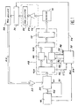
- a memory 10 are associated with selection circuits 12 which allow selection memory cells or cells and circuits reading 14 which allow to "collect” the signals read from memory cells as binary or data information.
- the addresses of memory cells or cells are supplied to circuits 12 by a so-called external address register 16A which receives them from a processing unit 18 by through an input / output circuit 20 and of a bidirectional bus 46.
- the external address register 16A and the circuits of selection 12 constitute the addressing circuits 48 of Memory.
- This input / output circuit 20 also receives the information or data read from memory 10 by through the reading circuits 14 and output amplifiers 22 and a bus unidirectional 44.
- the input / output circuit 20 is controlled by an OE signal supplied by the treatment 18 on a conductor 82.
- the read circuits 14 include 24 reading amplifiers which amplify the signals read from the selected memory cells and a read register 26 which records or stores under binary form the signals read.
- Memory 10 is also associated with circuits which will not be described here because the invention relates only to the reading of the memory.
- the addressing circuits 48 and the reading circuits 14 must be completed and modified.
- the internal address register 16B has its terminals outputs which are connected to the selection circuits 12 of memory and its input terminals which are connected to the output terminals of the address register external 16A via, on the one hand, the circuit 40 and, on the other hand, the comparator circuit 42.
- Reading register 26 is associated with a register additional said of data 28 which is connected between the read register 26 and the amplifiers exit.
- the input terminals of the data register 28 are connected to the output terminals of the reading 26 through circuits electronic 30 including electronic doors transfer.
- Data register output terminals 28 are connected to the input / output circuits 20 through output amplifiers 22 and of the unidirectional bus 44.
- the sequencing circuit 32 is connected to the processing 18, to the calculation circuit 40, to the circuit comparator 42 and to electronic circuits 30. It includes logic circuits and a clock circuit to develop the sequential control signals of the calculation circuit 40, comparator 42, registers 16A and 16B and electronic doors 30.
- the sequencing circuit 32 receives a certain number of signals which are listed ALE, ATD and IAE on conductors 84, 86 and 88, respectively. He gives control signals to comparator circuit 42, at calculation circuit 40 and electronic circuits 30 on conductors 90, 92 and 94.
- the ALE signal is a code validation signal address
- the ATD signal is a signal which indicates that the address code has just changed
- IAE is a signal which indicates the identity or not of the contents of registers 16A and 16B.
- the calculation circuit 40 performs the function of prediction so as to determine the addressing code next from previous address code contained in the address register 16A, this function corresponding to the one chosen by the programmer when programming the unit processing 18.
- This predictive function or law has as a result that the data that is used for the processing are not saved in addresses from memory but in addresses that seen from the outside, no logical link between them, the law of prediction not being known to the observer.
- the signal ATD (diamond 50) says of "Address Transition Detection” starts the cycle of reading.
- the first code addressing from the processing unit 18 via input / output circuits 20 is recorded in the external address register 16A (rectangle 52). This first address code is compared by the circuit comparator 42 to the code contained in the address register internal 16B (diamond 54).
- the code contained in the register 16B includes, for example, only digits "0" so the comparison indicates the absence of identity.
- This lack of identity drives the circuit of sequencing to provide at time (T0 + 20ns) a signal registration of the first address code in the internal address register 16B (rectangle 56).
- the first address code selects the memory 10 (rectangle 58).
- the memory reading is performed (rectangle 60).
- the signals read in the memory are recorded in binary form in the register of reading 26 (rectangle 62).
- the contents of the register internal 16B can be changed to save time (T0 + 80ns) the second address code calculated by the calculation circuit 40 (rectangle 68).
- the second address code selects the corresponding memory cells (rectangle 70).
- the memory cells selected are read (rectangle 72) and the signals read are saved in binary form in the time reading register (T0 + 130ns) (rectangle 74).
- the transfer of the contents of the register of reading 26 in the data register 28 is carried out at time (T0 + 20ns) (rectangle 78) of the second cycle in course, this content corresponding to that recorded at time (T0 + 130ns) (rectangle 74) of the first cycle, i.e. the previous cycle.
- the transfer of given to the processing unit is performed on time (T0 + 40ns) via the input / output circuit 20 (rectangle 80) under the control of the OE signal ( Figure 1).
- the operations defined by the rectangles 68,70,72 and 74 are made from second address code provided by the processing 18, which allows recording on time (T0 + 60ns) of this second cycle the content of the cells of memory selected by a third address code as calculated by the calculation circuit 40.
- Such a method of reading the memory 10 according to the operations (k) to (r) leads to the use of two registers 26 and 28 when reading but provides a gain of time and therefore a higher reading speed in average.
- the calculation operation (o) address code can start upon registration signals read in the read register 26 to provided that the address code resulting from the calculation is not registered in address register 16B only after the transfer of the data read from the register of reading in the address register.
- the start of operation (o) is inserted in operation (n) from recording the signals read in the register of reading 26.
Landscapes
- Engineering & Computer Science (AREA)
- Microelectronics & Electronic Packaging (AREA)
- Compression, Expansion, Code Conversion, And Decoders (AREA)
Applications Claiming Priority (2)
| Application Number | Priority Date | Filing Date | Title |
|---|---|---|---|
| FR9615515A FR2757306B1 (fr) | 1996-12-17 | 1996-12-17 | Procede et dispositif de lecture avec prediction d'une memoire |
| FR9615515 | 1996-12-17 |
Publications (2)
| Publication Number | Publication Date |
|---|---|
| EP0849740A1 true EP0849740A1 (de) | 1998-06-24 |
| EP0849740B1 EP0849740B1 (de) | 1999-10-20 |
Family
ID=9498767
Family Applications (1)
| Application Number | Title | Priority Date | Filing Date |
|---|---|---|---|
| EP97402807A Expired - Lifetime EP0849740B1 (de) | 1996-12-17 | 1997-11-21 | Leseverfahren und -anordnung mit Speicherprädiktion |
Country Status (4)
| Country | Link |
|---|---|
| US (1) | US6138220A (de) |
| EP (1) | EP0849740B1 (de) |
| DE (1) | DE69700649T2 (de) |
| FR (1) | FR2757306B1 (de) |
Families Citing this family (1)
| Publication number | Priority date | Publication date | Assignee | Title |
|---|---|---|---|---|
| US11409874B2 (en) * | 2019-07-03 | 2022-08-09 | International Business Machines Corporation | Coprocessor-accelerated verifiable computing |
Citations (3)
| Publication number | Priority date | Publication date | Assignee | Title |
|---|---|---|---|---|
| EP0315194A2 (de) * | 1987-11-04 | 1989-05-10 | Nec Corporation | Mikrocomputer, der fähig ist, ununterbrochen für kurze Zeit an Adressen zu gelangen |
| EP0333231A2 (de) * | 1988-03-18 | 1989-09-20 | Nec Corporation | Mikrocomputersystem, fähig zum Speicherzugriff mit hoher Geschwindigkeit |
| US4901227A (en) * | 1986-08-27 | 1990-02-13 | Nec Corporation | Microcomputer system |
Family Cites Families (5)
| Publication number | Priority date | Publication date | Assignee | Title |
|---|---|---|---|---|
| US4691277A (en) * | 1984-10-24 | 1987-09-01 | International Business Machines Corp. | Small instruction cache using branch target table to effect instruction prefetch |
| JPS6275860A (ja) * | 1985-09-30 | 1987-04-07 | Toshiba Corp | デ−タ転送制御装置 |
| AU665368B2 (en) * | 1992-02-27 | 1996-01-04 | Samsung Electronics Co., Ltd. | CPU having pipelined instruction unit and effective address calculation unit with retained virtual address capability |
| JP3435783B2 (ja) * | 1994-03-17 | 2003-08-11 | 株式会社日立製作所 | 複数組のデータバッファを備える記憶素子及び記憶素子を用いたデータ処理システム |
| JP3170146B2 (ja) * | 1994-07-29 | 2001-05-28 | 株式会社東芝 | 半導体記憶装置 |
-
1996
- 1996-12-17 FR FR9615515A patent/FR2757306B1/fr not_active Expired - Fee Related
-
1997
- 1997-11-21 DE DE69700649T patent/DE69700649T2/de not_active Expired - Fee Related
- 1997-11-21 EP EP97402807A patent/EP0849740B1/de not_active Expired - Lifetime
- 1997-12-16 US US08/991,693 patent/US6138220A/en not_active Expired - Lifetime
Patent Citations (3)
| Publication number | Priority date | Publication date | Assignee | Title |
|---|---|---|---|---|
| US4901227A (en) * | 1986-08-27 | 1990-02-13 | Nec Corporation | Microcomputer system |
| EP0315194A2 (de) * | 1987-11-04 | 1989-05-10 | Nec Corporation | Mikrocomputer, der fähig ist, ununterbrochen für kurze Zeit an Adressen zu gelangen |
| EP0333231A2 (de) * | 1988-03-18 | 1989-09-20 | Nec Corporation | Mikrocomputersystem, fähig zum Speicherzugriff mit hoher Geschwindigkeit |
Also Published As
| Publication number | Publication date |
|---|---|
| US6138220A (en) | 2000-10-24 |
| DE69700649D1 (de) | 1999-11-25 |
| FR2757306A1 (fr) | 1998-06-19 |
| EP0849740B1 (de) | 1999-10-20 |
| FR2757306B1 (fr) | 1999-01-15 |
| DE69700649T2 (de) | 2000-06-08 |
Similar Documents
| Publication | Publication Date | Title |
|---|---|---|
| EP0683454B1 (de) | Verfahren zur Überwachung des Programmablaufs | |
| FR2606903A1 (fr) | Procede et dispositif de gestion de points d'arret dans un moniteur de logiciel | |
| EP0913765A1 (de) | Prozessor mit Steuerung von wiederholbaren oder Mehrzyklus-Befehlen | |
| FR2589264A1 (fr) | Micro-ordinateur a deux modes de fonctionnement | |
| FR2672709A1 (fr) | Machine d'etat d'ordre. | |
| EP0889429B1 (de) | Chipkartenleser unter Verwendung eines schnellen Übertragungsprotokolls | |
| EP0166838B1 (de) | Verfahren und Anordnung zur Detektion einer besonderen Bitkonfiguration in einem seriellen Bitstrom | |
| BE897587A (fr) | Circuit parallele de controle de redondance cyclique | |
| FR2508669A1 (fr) | Dispositif logique programmable de prise, traitement et transmission de donnees | |
| CH621201A5 (de) | ||
| EP0849740B1 (de) | Leseverfahren und -anordnung mit Speicherprädiktion | |
| FR2543710A1 (fr) | Systeme de traitement d'images de figures | |
| FR2595474A1 (fr) | Dispositif de controle et de verification du fonctionnement de blocs internes a un circuit integre | |
| EP0849739B1 (de) | Anordnung und Verfahren zum inkrementellen Lesen eines Speichers | |
| EP0043745B1 (de) | Digitales Datenverarbeitungs- und Speichersystem, insbesondere für ein Tomodensitometer | |
| EP0193417A1 (de) | Vorrichtung zur Datenauswechslung zwischen einem Computer und einer peripheren Einheit | |
| FR2587519A1 (fr) | Agencement de changement de mode permettant de changer selectivement des modes d'exploitation d'un systeme de machine virtuelle | |
| EP0733977B1 (de) | Rechnersystem mit hierarchischen Speichern | |
| CH631018A5 (en) | Data processing installation | |
| FR2741497A1 (fr) | Systeme d'envoi de cellule atm | |
| FR2659763A1 (fr) | Systeme d'ordinateur, source de programme et procede de validation selective de fonctions dans un tel systeme d'ordinateur. | |
| EP0449190B1 (de) | Programmschalteinrichtung zur Erzeugung von binären Ausgangssignalen als Reaktion auf ein Taktsignal | |
| FR2531792A1 (fr) | Coupleur d'interface entre un micro-processeur central et un automatiseur comportant une pluralite d'axes de commande | |
| FR2770661A1 (fr) | Microprocesseur comprenant des moyens de concatenation de bits | |
| FR2582423A1 (fr) | Memoire tampon a interposer entre deux systemes synchrones a vitesses differentes |
Legal Events
| Date | Code | Title | Description |
|---|---|---|---|
| PUAI | Public reference made under article 153(3) epc to a published international application that has entered the european phase |
Free format text: ORIGINAL CODE: 0009012 |
|
| AK | Designated contracting states |
Kind code of ref document: A1 Designated state(s): DE FR GB IT |
|
| AX | Request for extension of the european patent |
Free format text: AL;LT;LV;MK;RO;SI |
|
| 17P | Request for examination filed |
Effective date: 19980715 |
|
| RAP3 | Party data changed (applicant data changed or rights of an application transferred) |
Owner name: STMICROELECTRONICS S.A. |
|
| GRAG | Despatch of communication of intention to grant |
Free format text: ORIGINAL CODE: EPIDOS AGRA |
|
| GRAG | Despatch of communication of intention to grant |
Free format text: ORIGINAL CODE: EPIDOS AGRA |
|
| AKX | Designation fees paid |
Free format text: DE FR GB IT |
|
| RBV | Designated contracting states (corrected) |
Designated state(s): DE FR GB IT |
|
| 17Q | First examination report despatched |
Effective date: 19990303 |
|
| GRAG | Despatch of communication of intention to grant |
Free format text: ORIGINAL CODE: EPIDOS AGRA |
|
| GRAH | Despatch of communication of intention to grant a patent |
Free format text: ORIGINAL CODE: EPIDOS IGRA |
|
| GRAH | Despatch of communication of intention to grant a patent |
Free format text: ORIGINAL CODE: EPIDOS IGRA |
|
| GRAA | (expected) grant |
Free format text: ORIGINAL CODE: 0009210 |
|
| AK | Designated contracting states |
Kind code of ref document: B1 Designated state(s): DE FR GB IT |
|
| GBT | Gb: translation of ep patent filed (gb section 77(6)(a)/1977) |
Effective date: 19991021 |
|
| REF | Corresponds to: |
Ref document number: 69700649 Country of ref document: DE Date of ref document: 19991125 |
|
| ITF | It: translation for a ep patent filed | ||
| PLBE | No opposition filed within time limit |
Free format text: ORIGINAL CODE: 0009261 |
|
| STAA | Information on the status of an ep patent application or granted ep patent |
Free format text: STATUS: NO OPPOSITION FILED WITHIN TIME LIMIT |
|
| 26N | No opposition filed | ||
| REG | Reference to a national code |
Ref country code: GB Ref legal event code: IF02 |
|
| PGFP | Annual fee paid to national office [announced via postgrant information from national office to epo] |
Ref country code: DE Payment date: 20031204 Year of fee payment: 7 |
|
| PG25 | Lapsed in a contracting state [announced via postgrant information from national office to epo] |
Ref country code: DE Free format text: LAPSE BECAUSE OF NON-PAYMENT OF DUE FEES Effective date: 20050601 |
|
| PGFP | Annual fee paid to national office [announced via postgrant information from national office to epo] |
Ref country code: FR Payment date: 20051108 Year of fee payment: 9 |
|
| PGFP | Annual fee paid to national office [announced via postgrant information from national office to epo] |
Ref country code: GB Payment date: 20051116 Year of fee payment: 9 |
|
| PG25 | Lapsed in a contracting state [announced via postgrant information from national office to epo] |
Ref country code: IT Free format text: LAPSE BECAUSE OF NON-PAYMENT OF DUE FEES;WARNING: LAPSES OF ITALIAN PATENTS WITH EFFECTIVE DATE BEFORE 2007 MAY HAVE OCCURRED AT ANY TIME BEFORE 2007. THE CORRECT EFFECTIVE DATE MAY BE DIFFERENT FROM THE ONE RECORDED. Effective date: 20051121 |
|
| GBPC | Gb: european patent ceased through non-payment of renewal fee |
Effective date: 20061121 |
|
| REG | Reference to a national code |
Ref country code: FR Ref legal event code: ST Effective date: 20070731 |
|
| PG25 | Lapsed in a contracting state [announced via postgrant information from national office to epo] |
Ref country code: GB Free format text: LAPSE BECAUSE OF NON-PAYMENT OF DUE FEES Effective date: 20061121 |
|
| PG25 | Lapsed in a contracting state [announced via postgrant information from national office to epo] |
Ref country code: FR Free format text: LAPSE BECAUSE OF NON-PAYMENT OF DUE FEES Effective date: 20061130 |