EP0847084A2 - Electronic modules manufacturing - Google Patents
Electronic modules manufacturing Download PDFInfo
- Publication number
- EP0847084A2 EP0847084A2 EP97306436A EP97306436A EP0847084A2 EP 0847084 A2 EP0847084 A2 EP 0847084A2 EP 97306436 A EP97306436 A EP 97306436A EP 97306436 A EP97306436 A EP 97306436A EP 0847084 A2 EP0847084 A2 EP 0847084A2
- Authority
- EP
- European Patent Office
- Prior art keywords
- module
- flat
- electronic module
- flat feature
- electronic
- Prior art date
- Legal status (The legal status is an assumption and is not a legal conclusion. Google has not performed a legal analysis and makes no representation as to the accuracy of the status listed.)
- Withdrawn
Links
Images


Classifications
-
- H—ELECTRICITY
- H01—ELECTRIC ELEMENTS
- H01L—SEMICONDUCTOR DEVICES NOT COVERED BY CLASS H10
- H01L21/00—Processes or apparatus adapted for the manufacture or treatment of semiconductor or solid state devices or of parts thereof
- H01L21/67—Apparatus specially adapted for handling semiconductor or electric solid state devices during manufacture or treatment thereof; Apparatus specially adapted for handling wafers during manufacture or treatment of semiconductor or electric solid state devices or components ; Apparatus not specifically provided for elsewhere
- H01L21/683—Apparatus specially adapted for handling semiconductor or electric solid state devices during manufacture or treatment thereof; Apparatus specially adapted for handling wafers during manufacture or treatment of semiconductor or electric solid state devices or components ; Apparatus not specifically provided for elsewhere for supporting or gripping
- H01L21/6835—Apparatus specially adapted for handling semiconductor or electric solid state devices during manufacture or treatment thereof; Apparatus specially adapted for handling wafers during manufacture or treatment of semiconductor or electric solid state devices or components ; Apparatus not specifically provided for elsewhere for supporting or gripping using temporarily an auxiliary support
-
- H—ELECTRICITY
- H01—ELECTRIC ELEMENTS
- H01L—SEMICONDUCTOR DEVICES NOT COVERED BY CLASS H10
- H01L23/00—Details of semiconductor or other solid state devices
- H01L23/28—Encapsulations, e.g. encapsulating layers, coatings, e.g. for protection
- H01L23/31—Encapsulations, e.g. encapsulating layers, coatings, e.g. for protection characterised by the arrangement or shape
- H01L23/3107—Encapsulations, e.g. encapsulating layers, coatings, e.g. for protection characterised by the arrangement or shape the device being completely enclosed
- H01L23/3121—Encapsulations, e.g. encapsulating layers, coatings, e.g. for protection characterised by the arrangement or shape the device being completely enclosed a substrate forming part of the encapsulation
- H01L23/3128—Encapsulations, e.g. encapsulating layers, coatings, e.g. for protection characterised by the arrangement or shape the device being completely enclosed a substrate forming part of the encapsulation the substrate having spherical bumps for external connection
-
- H—ELECTRICITY
- H05—ELECTRIC TECHNIQUES NOT OTHERWISE PROVIDED FOR
- H05K—PRINTED CIRCUITS; CASINGS OR CONSTRUCTIONAL DETAILS OF ELECTRIC APPARATUS; MANUFACTURE OF ASSEMBLAGES OF ELECTRICAL COMPONENTS
- H05K3/00—Apparatus or processes for manufacturing printed circuits
- H05K3/30—Assembling printed circuits with electric components, e.g. with resistor
- H05K3/303—Surface mounted components, e.g. affixing before soldering, aligning means, spacing means
-
- H—ELECTRICITY
- H01—ELECTRIC ELEMENTS
- H01L—SEMICONDUCTOR DEVICES NOT COVERED BY CLASS H10
- H01L2224/00—Indexing scheme for arrangements for connecting or disconnecting semiconductor or solid-state bodies and methods related thereto as covered by H01L24/00
- H01L2224/01—Means for bonding being attached to, or being formed on, the surface to be connected, e.g. chip-to-package, die-attach, "first-level" interconnects; Manufacturing methods related thereto
- H01L2224/42—Wire connectors; Manufacturing methods related thereto
- H01L2224/47—Structure, shape, material or disposition of the wire connectors after the connecting process
- H01L2224/48—Structure, shape, material or disposition of the wire connectors after the connecting process of an individual wire connector
- H01L2224/4805—Shape
- H01L2224/4809—Loop shape
- H01L2224/48091—Arched
-
- H—ELECTRICITY
- H01—ELECTRIC ELEMENTS
- H01L—SEMICONDUCTOR DEVICES NOT COVERED BY CLASS H10
- H01L2224/00—Indexing scheme for arrangements for connecting or disconnecting semiconductor or solid-state bodies and methods related thereto as covered by H01L24/00
- H01L2224/01—Means for bonding being attached to, or being formed on, the surface to be connected, e.g. chip-to-package, die-attach, "first-level" interconnects; Manufacturing methods related thereto
- H01L2224/42—Wire connectors; Manufacturing methods related thereto
- H01L2224/47—Structure, shape, material or disposition of the wire connectors after the connecting process
- H01L2224/48—Structure, shape, material or disposition of the wire connectors after the connecting process of an individual wire connector
- H01L2224/481—Disposition
- H01L2224/48151—Connecting between a semiconductor or solid-state body and an item not being a semiconductor or solid-state body, e.g. chip-to-substrate, chip-to-passive
- H01L2224/48221—Connecting between a semiconductor or solid-state body and an item not being a semiconductor or solid-state body, e.g. chip-to-substrate, chip-to-passive the body and the item being stacked
- H01L2224/48225—Connecting between a semiconductor or solid-state body and an item not being a semiconductor or solid-state body, e.g. chip-to-substrate, chip-to-passive the body and the item being stacked the item being non-metallic, e.g. insulating substrate with or without metallisation
- H01L2224/48227—Connecting between a semiconductor or solid-state body and an item not being a semiconductor or solid-state body, e.g. chip-to-substrate, chip-to-passive the body and the item being stacked the item being non-metallic, e.g. insulating substrate with or without metallisation connecting the wire to a bond pad of the item
-
- H—ELECTRICITY
- H01—ELECTRIC ELEMENTS
- H01L—SEMICONDUCTOR DEVICES NOT COVERED BY CLASS H10
- H01L24/00—Arrangements for connecting or disconnecting semiconductor or solid-state bodies; Methods or apparatus related thereto
- H01L24/01—Means for bonding being attached to, or being formed on, the surface to be connected, e.g. chip-to-package, die-attach, "first-level" interconnects; Manufacturing methods related thereto
- H01L24/42—Wire connectors; Manufacturing methods related thereto
- H01L24/47—Structure, shape, material or disposition of the wire connectors after the connecting process
- H01L24/48—Structure, shape, material or disposition of the wire connectors after the connecting process of an individual wire connector
-
- H—ELECTRICITY
- H01—ELECTRIC ELEMENTS
- H01L—SEMICONDUCTOR DEVICES NOT COVERED BY CLASS H10
- H01L2924/00—Indexing scheme for arrangements or methods for connecting or disconnecting semiconductor or solid-state bodies as covered by H01L24/00
- H01L2924/0001—Technical content checked by a classifier
- H01L2924/00014—Technical content checked by a classifier the subject-matter covered by the group, the symbol of which is combined with the symbol of this group, being disclosed without further technical details
-
- H—ELECTRICITY
- H01—ELECTRIC ELEMENTS
- H01L—SEMICONDUCTOR DEVICES NOT COVERED BY CLASS H10
- H01L2924/00—Indexing scheme for arrangements or methods for connecting or disconnecting semiconductor or solid-state bodies as covered by H01L24/00
- H01L2924/10—Details of semiconductor or other solid state devices to be connected
- H01L2924/102—Material of the semiconductor or solid state bodies
- H01L2924/1025—Semiconducting materials
- H01L2924/10251—Elemental semiconductors, i.e. Group IV
- H01L2924/10253—Silicon [Si]
-
- H—ELECTRICITY
- H01—ELECTRIC ELEMENTS
- H01L—SEMICONDUCTOR DEVICES NOT COVERED BY CLASS H10
- H01L2924/00—Indexing scheme for arrangements or methods for connecting or disconnecting semiconductor or solid-state bodies as covered by H01L24/00
- H01L2924/15—Details of package parts other than the semiconductor or other solid state devices to be connected
- H01L2924/151—Die mounting substrate
- H01L2924/153—Connection portion
- H01L2924/1531—Connection portion the connection portion being formed only on the surface of the substrate opposite to the die mounting surface
- H01L2924/15311—Connection portion the connection portion being formed only on the surface of the substrate opposite to the die mounting surface being a ball array, e.g. BGA
-
- H—ELECTRICITY
- H01—ELECTRIC ELEMENTS
- H01L—SEMICONDUCTOR DEVICES NOT COVERED BY CLASS H10
- H01L2924/00—Indexing scheme for arrangements or methods for connecting or disconnecting semiconductor or solid-state bodies as covered by H01L24/00
- H01L2924/15—Details of package parts other than the semiconductor or other solid state devices to be connected
- H01L2924/181—Encapsulation
-
- H—ELECTRICITY
- H01—ELECTRIC ELEMENTS
- H01L—SEMICONDUCTOR DEVICES NOT COVERED BY CLASS H10
- H01L2924/00—Indexing scheme for arrangements or methods for connecting or disconnecting semiconductor or solid-state bodies as covered by H01L24/00
- H01L2924/30—Technical effects
- H01L2924/301—Electrical effects
- H01L2924/3025—Electromagnetic shielding
-
- H—ELECTRICITY
- H05—ELECTRIC TECHNIQUES NOT OTHERWISE PROVIDED FOR
- H05K—PRINTED CIRCUITS; CASINGS OR CONSTRUCTIONAL DETAILS OF ELECTRIC APPARATUS; MANUFACTURE OF ASSEMBLAGES OF ELECTRICAL COMPONENTS
- H05K1/00—Printed circuits
- H05K1/02—Details
- H05K1/14—Structural association of two or more printed circuits
- H05K1/141—One or more single auxiliary printed circuits mounted on a main printed circuit, e.g. modules, adapters
-
- H—ELECTRICITY
- H05—ELECTRIC TECHNIQUES NOT OTHERWISE PROVIDED FOR
- H05K—PRINTED CIRCUITS; CASINGS OR CONSTRUCTIONAL DETAILS OF ELECTRIC APPARATUS; MANUFACTURE OF ASSEMBLAGES OF ELECTRICAL COMPONENTS
- H05K2201/00—Indexing scheme relating to printed circuits covered by H05K1/00
- H05K2201/10—Details of components or other objects attached to or integrated in a printed circuit board
- H05K2201/10431—Details of mounted components
- H05K2201/10568—Integral adaptations of a component or an auxiliary PCB for mounting, e.g. integral spacer element
-
- H—ELECTRICITY
- H05—ELECTRIC TECHNIQUES NOT OTHERWISE PROVIDED FOR
- H05K—PRINTED CIRCUITS; CASINGS OR CONSTRUCTIONAL DETAILS OF ELECTRIC APPARATUS; MANUFACTURE OF ASSEMBLAGES OF ELECTRICAL COMPONENTS
- H05K2201/00—Indexing scheme relating to printed circuits covered by H05K1/00
- H05K2201/10—Details of components or other objects attached to or integrated in a printed circuit board
- H05K2201/10613—Details of electrical connections of non-printed components, e.g. special leads
- H05K2201/10621—Components characterised by their electrical contacts
- H05K2201/10734—Ball grid array [BGA]; Bump grid array
-
- H—ELECTRICITY
- H05—ELECTRIC TECHNIQUES NOT OTHERWISE PROVIDED FOR
- H05K—PRINTED CIRCUITS; CASINGS OR CONSTRUCTIONAL DETAILS OF ELECTRIC APPARATUS; MANUFACTURE OF ASSEMBLAGES OF ELECTRICAL COMPONENTS
- H05K2203/00—Indexing scheme relating to apparatus or processes for manufacturing printed circuits covered by H05K3/00
- H05K2203/01—Tools for processing; Objects used during processing
- H05K2203/0195—Tool for a process not provided for in H05K3/00, e.g. tool for handling objects using suction, for deforming objects, for applying local pressure
-
- H—ELECTRICITY
- H05—ELECTRIC TECHNIQUES NOT OTHERWISE PROVIDED FOR
- H05K—PRINTED CIRCUITS; CASINGS OR CONSTRUCTIONAL DETAILS OF ELECTRIC APPARATUS; MANUFACTURE OF ASSEMBLAGES OF ELECTRICAL COMPONENTS
- H05K2203/00—Indexing scheme relating to apparatus or processes for manufacturing printed circuits covered by H05K3/00
- H05K2203/08—Treatments involving gases
- H05K2203/082—Suction, e.g. for holding solder balls or components
-
- Y—GENERAL TAGGING OF NEW TECHNOLOGICAL DEVELOPMENTS; GENERAL TAGGING OF CROSS-SECTIONAL TECHNOLOGIES SPANNING OVER SEVERAL SECTIONS OF THE IPC; TECHNICAL SUBJECTS COVERED BY FORMER USPC CROSS-REFERENCE ART COLLECTIONS [XRACs] AND DIGESTS
- Y02—TECHNOLOGIES OR APPLICATIONS FOR MITIGATION OR ADAPTATION AGAINST CLIMATE CHANGE
- Y02P—CLIMATE CHANGE MITIGATION TECHNOLOGIES IN THE PRODUCTION OR PROCESSING OF GOODS
- Y02P70/00—Climate change mitigation technologies in the production process for final industrial or consumer products
- Y02P70/50—Manufacturing or production processes characterised by the final manufactured product
-
- Y—GENERAL TAGGING OF NEW TECHNOLOGICAL DEVELOPMENTS; GENERAL TAGGING OF CROSS-SECTIONAL TECHNOLOGIES SPANNING OVER SEVERAL SECTIONS OF THE IPC; TECHNICAL SUBJECTS COVERED BY FORMER USPC CROSS-REFERENCE ART COLLECTIONS [XRACs] AND DIGESTS
- Y10—TECHNICAL SUBJECTS COVERED BY FORMER USPC
- Y10S—TECHNICAL SUBJECTS COVERED BY FORMER USPC CROSS-REFERENCE ART COLLECTIONS [XRACs] AND DIGESTS
- Y10S439/00—Electrical connectors
- Y10S439/94—Electrical connectors including provision for mechanical lifting or manipulation, e.g. for vacuum lifting
Definitions
- the present invention relates to the manufacturing of electronic modules and more particularly to a method for improving the handling of the modules during manufacturing processes.
- PCBGA Plastic Ball Grid Array
- SCM Single Chip Module
- MCM Multi Chip Module
- These modules are provided with a plurality of conductive pads for the electrical connection with electronic circuits (such as mother boards, back planes, application boards).
- the electrical connection is achieved by little spherical portions of solder alloy which give the name of Ball Grid Array (BGA) to this kind of electronic module.
- BGA Ball Grid Array
- These modules are usually called Plastic Ball Grid Array.
- the definition "Plastic” indicates the flexible nature of the PCB as opposed to a ceramic substrate.
- Fig. 1 is an example of a section of a BGA module of the MCM type.
- the Blob Top also called Glob Top
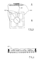
- Fig. 2 is a top view of the package of Fig. 1.
- the temperature at which the resins for the encapsulants are dispensed is higher than the utilisation temperature and the resins usually reduce their volume after polymerisation. This means that the temperature decrease causes a shrinkage of the resins which determines a tension build up in the module when it is cooled from the processing temperature down to the room temperature; the module at the end of the assembly presents a deformation with the four corners of the laminate lifted with respect to the centre.
- This is the above mentioned warpage effect, which can impact long term reliability of the module and cause problems in card assembly because of the non-coplanarity of the balls or leads: peripheral balls or leads might not touch solder screen printed on the board thus leading to an open circuit condition after reflow.
- each single silicon chip assembled on a MCM module must be separately covered with a resin cap in the way described above thus obtaining a non flat top surface with a plurality of distributed glob top mounds.
- an electronic module having a non-flat top surface characterized in that it further comprises a flat feature for facilitating the automatic picking of the module during the manufacturing process.
- a flat feature is added to an electronic module in order to allow to be picked with standard picking means requiring flat surfaces.
- This flat feature can be realised with different shapes and materials and attached to the module with different methods to fit different module shapes and satisfy different requirements.
- a preferred embodiment of the present invention is shown.
- On the MCM module represented four components 103 are attached on the substrate and each one is covered by a protective resin cap of irregular shape.
- a protective resin cap of irregular shape In the middle of the module substrate there is a portion free from components where a mushroom shaped stud is placed.
- This mushroom stud can be either permanently fixed (e.g. glued) or removably attached (e.g. press fitted) on the module.
- the flat surface allows the module to be picked up by a vacuum pick up machine or by all the picking tools requiring a flat surface. In case of press fitting, the stud can be easily removed after assembly of the module in order to reduce the profile of the final package. This is particularly useful when space saving is a critical requirement.
- Fig. 4 shows a different embodiment of the present invention. In this case a free central portion is not available.
- a round cap 401 as also represented in Fig. 5 is used.
- the cap 401 is connected to the module substrate 101 through four spacers positioned along the four sides of the substrate 101 in the middle. This position should minimise the impact of the module warpage on the disc.
- the cap is press fitted and then removable, but could as well be glued or permanently fixed in any different way (e.g. rivetted).
- the material used for the manufacture of the stud or the cap of the preferred embodiments described above can be any light weight material (e.g. plastic), but in case the MCM module has a high generation of heat a highly thermal conductive material could be employed. In this way the cap or the stud work as finned heat sinks.
- the space between the cap and the electronic components can also be filled with resin or thermal grease.
- a RFI (Radio Frequency Interference) shield can be realised by connecting the metal disc to the Ground signal plane/network.
- a Fraday Cage could also be realised.
- cap 401 Another possible additional use of the cap 401 is to print on it the identification data of the module, otherwise very difficult to be placed in case of a plurality of distributed glob top mounds.
Landscapes
- Engineering & Computer Science (AREA)
- Microelectronics & Electronic Packaging (AREA)
- Power Engineering (AREA)
- Condensed Matter Physics & Semiconductors (AREA)
- General Physics & Mathematics (AREA)
- Computer Hardware Design (AREA)
- Physics & Mathematics (AREA)
- Manufacturing & Machinery (AREA)
- Encapsulation Of And Coatings For Semiconductor Or Solid State Devices (AREA)
- Piezo-Electric Or Mechanical Vibrators, Or Delay Or Filter Circuits (AREA)
- Structures Or Materials For Encapsulating Or Coating Semiconductor Devices Or Solid State Devices (AREA)
- Solid State Image Pick-Up Elements (AREA)
- Casings For Electric Apparatus (AREA)
- Packaging Frangible Articles (AREA)
- Surface Acoustic Wave Elements And Circuit Networks Thereof (AREA)
Abstract
Description
Claims (14)
- An electronic module having a non-flat top surface characterized in that it further comprises a flat feature (301, 401) for facilitating the automatic picking of the module during the manufacturing process.
- The electronic module of claim 1 wherein the flat feature is mushroom shaped (301).
- The electronic module of any preceding claim wherein the flat feature (301, 401) is positioned in a central portion of the module.
- The electronic module of claim 1 wherein the flat feature has substantially the shape of a disc (401).
- The electronic module of any preceding claim wherein the flat feature (301, 401) is attached to the module substrate by means of a plurality of spacers.
- The electronic module of any preceding claim wherein the flat feature (301, 401) is removable.
- The electronic module of any preceding claim wherein the flat feature (301, 401) is of plastic material.
- The electronic module of any preceding claim wherein the flat feature (301, 401) is of highly thermal conductive material.
- The electronic module of any preceding claim wherein the module is of the Ball Grid Array (BGA) type.
- The electronic module of claim 9 wherein the module is of the Multi Chip Module (MCM) type.
- The electronic module of any preceding claim wherein the flat feature is separated by the active components by means of resin.
- A method, in the manufacturing of electronic modules having a non flat top surface, of adding a flat feature (301, 401) for facilitating the automatic picking of the module by means of picking tools.
- The method of claim 12 wherein the flat feature (301, 401) is removable.
- The method of claim 12 or 13 further comprising the step of picking and moving the module by means of a vacuum pick up tool.
Applications Claiming Priority (2)
| Application Number | Priority Date | Filing Date | Title |
|---|---|---|---|
| GB9625233 | 1996-12-04 | ||
| GB9625233A GB2320132A (en) | 1996-12-04 | 1996-12-04 | Handling electronic modules |
Publications (2)
| Publication Number | Publication Date |
|---|---|
| EP0847084A2 true EP0847084A2 (en) | 1998-06-10 |
| EP0847084A3 EP0847084A3 (en) | 1999-01-20 |
Family
ID=10803955
Family Applications (1)
| Application Number | Title | Priority Date | Filing Date |
|---|---|---|---|
| EP97306436A Withdrawn EP0847084A3 (en) | 1996-12-04 | 1997-08-22 | Electronic modules manufacturing |
Country Status (7)
| Country | Link |
|---|---|
| US (1) | US6049464A (en) |
| EP (1) | EP0847084A3 (en) |
| CN (1) | CN1123931C (en) |
| CA (1) | CA2222602C (en) |
| GB (1) | GB2320132A (en) |
| MY (1) | MY117869A (en) |
| SG (1) | SG55406A1 (en) |
Cited By (2)
| Publication number | Priority date | Publication date | Assignee | Title |
|---|---|---|---|---|
| DE19948295C1 (en) * | 1999-10-06 | 2001-06-21 | Bosch Gmbh Robert | Automatic circuit board assembly method has mounting adapter fitted to component for facilitating handling via standard automatic assembly device |
| US7070085B2 (en) | 2003-01-07 | 2006-07-04 | International Business Machines Corporation | Water soluble protective paste for manufacturing printed circuit boards |
Families Citing this family (5)
| Publication number | Priority date | Publication date | Assignee | Title |
|---|---|---|---|---|
| US6462271B2 (en) | 2000-12-27 | 2002-10-08 | International Business Machines Corporation | Capping structure for electronics package undergoing compressive socket actuation |
| US7255601B2 (en) * | 2004-12-21 | 2007-08-14 | Fci Americas Technology, Inc. | Cap for an electrical connector |
| US7264488B2 (en) * | 2006-01-03 | 2007-09-04 | Fci Americas Technology, Inc. | Pickup cap for electrical connector |
| US20080113532A1 (en) * | 2006-11-13 | 2008-05-15 | David Christopher Smeltz | Pick-and-place card guide clip-on grounding members |
| US8337219B2 (en) | 2011-02-19 | 2012-12-25 | Laird Technologies, Inc. | Card guide grounding strips |
Citations (4)
| Publication number | Priority date | Publication date | Assignee | Title |
|---|---|---|---|---|
| US4837184A (en) * | 1988-01-04 | 1989-06-06 | Motorola Inc. | Process of making an electronic device package with peripheral carrier structure of low-cost plastic |
| DE4340594A1 (en) * | 1992-12-01 | 1994-06-09 | Murata Manufacturing Co | Electronic surface mount device - has electronic element with exposed flat surface in its upper region for drawing up device with suction nozzle |
| EP0675538A2 (en) * | 1994-03-31 | 1995-10-04 | STMicroelectronics, Inc. | Integrated circuit package with flat topped heat sink |
| DE29617668U1 (en) * | 1996-10-10 | 1996-12-05 | Hagn, Erwin, 85368 Moosburg | Device for producing a suction surface on an object and electrical component formed thereby |
Family Cites Families (10)
| Publication number | Priority date | Publication date | Assignee | Title |
|---|---|---|---|---|
| US4667944A (en) * | 1985-08-29 | 1987-05-26 | Vichem Corporation | Means for handling semiconductor die and the like |
| US5055971A (en) * | 1989-12-21 | 1991-10-08 | At&T Bell Laboratories | Magnetic component using core clip arrangement operative for facilitating pick and place surface mount |
| JPH0744079Y2 (en) * | 1991-12-09 | 1995-10-09 | モレックス インコーポレーテッド | Surface mount connector auto mount cover |
| US5383797A (en) * | 1993-07-08 | 1995-01-24 | Molex Incorporated | System for handling electrical connectors by a vacuum-suction nozzle |
| GB9407137D0 (en) * | 1994-04-11 | 1994-06-01 | Amp Gmbh | Electrical connector suction platform for facilitating picking |
| US5507657A (en) * | 1994-09-23 | 1996-04-16 | Molex Incorporated | Electrical connector cover |
| GB2294678A (en) * | 1994-10-20 | 1996-05-08 | Thomas & Betts Corp | Methods of enabling articles to be transported |
| JP3014608U (en) * | 1994-12-07 | 1995-08-15 | モレックス インコーポレーテッド | Adsorption member for transporting connector |
| US5681174A (en) * | 1995-12-21 | 1997-10-28 | The Whitaker Corporation | Electrical connector with releasable positioning cover |
| US5694300A (en) * | 1996-04-01 | 1997-12-02 | Northrop Grumman Corporation | Electromagnetically channelized microwave integrated circuit |
-
1996
- 1996-12-04 GB GB9625233A patent/GB2320132A/en not_active Withdrawn
-
1997
- 1997-08-22 EP EP97306436A patent/EP0847084A3/en not_active Withdrawn
- 1997-11-03 CN CN97122453A patent/CN1123931C/en not_active Expired - Fee Related
- 1997-11-03 SG SG1997003942A patent/SG55406A1/en unknown
- 1997-11-03 MY MYPI97005190A patent/MY117869A/en unknown
- 1997-11-25 US US08/978,303 patent/US6049464A/en not_active Expired - Fee Related
- 1997-11-27 CA CA002222602A patent/CA2222602C/en not_active Expired - Fee Related
Patent Citations (4)
| Publication number | Priority date | Publication date | Assignee | Title |
|---|---|---|---|---|
| US4837184A (en) * | 1988-01-04 | 1989-06-06 | Motorola Inc. | Process of making an electronic device package with peripheral carrier structure of low-cost plastic |
| DE4340594A1 (en) * | 1992-12-01 | 1994-06-09 | Murata Manufacturing Co | Electronic surface mount device - has electronic element with exposed flat surface in its upper region for drawing up device with suction nozzle |
| EP0675538A2 (en) * | 1994-03-31 | 1995-10-04 | STMicroelectronics, Inc. | Integrated circuit package with flat topped heat sink |
| DE29617668U1 (en) * | 1996-10-10 | 1996-12-05 | Hagn, Erwin, 85368 Moosburg | Device for producing a suction surface on an object and electrical component formed thereby |
Cited By (2)
| Publication number | Priority date | Publication date | Assignee | Title |
|---|---|---|---|---|
| DE19948295C1 (en) * | 1999-10-06 | 2001-06-21 | Bosch Gmbh Robert | Automatic circuit board assembly method has mounting adapter fitted to component for facilitating handling via standard automatic assembly device |
| US7070085B2 (en) | 2003-01-07 | 2006-07-04 | International Business Machines Corporation | Water soluble protective paste for manufacturing printed circuit boards |
Also Published As
| Publication number | Publication date |
|---|---|
| US6049464A (en) | 2000-04-11 |
| MY117869A (en) | 2004-08-30 |
| SG55406A1 (en) | 1998-12-21 |
| GB9625233D0 (en) | 1997-01-22 |
| CN1190799A (en) | 1998-08-19 |
| CA2222602A1 (en) | 1998-06-04 |
| CN1123931C (en) | 2003-10-08 |
| GB2320132A (en) | 1998-06-10 |
| EP0847084A3 (en) | 1999-01-20 |
| CA2222602C (en) | 2003-06-24 |
Similar Documents
| Publication | Publication Date | Title |
|---|---|---|
| US9472485B2 (en) | Hybrid thermal interface material for IC packages with integrated heat spreader | |
| EP0729180B1 (en) | Packaging multi-chip modules without wirebond interconnection | |
| KR100734816B1 (en) | Optimized lid mounting for electronic device carriers | |
| US7211889B2 (en) | Semiconductor package and method for manufacturing the same | |
| US6639324B1 (en) | Flip chip package module and method of forming the same | |
| US6570259B2 (en) | Apparatus to reduce thermal fatigue stress on flip chip solder connections | |
| US7300822B2 (en) | Low warpage flip chip package solution-channel heat spreader | |
| US20090127700A1 (en) | Thermal conductor lids for area array packaged multi-chip modules and methods to dissipate heat from multi-chip modules | |
| US7112882B2 (en) | Structures and methods for heat dissipation of semiconductor integrated circuits | |
| CN107978569B (en) | Chip packaging structure and manufacturing method thereof | |
| EP1429377B1 (en) | Method of reflowing conductive terminals | |
| US6049464A (en) | Electronic modules manufacturing | |
| US20050121757A1 (en) | Integrated circuit package overlay | |
| US20050093153A1 (en) | BGA package with component protection on bottom | |
| KR100294602B1 (en) | Electronic ball grid array module with solder pads of different sizes | |
| US20040080033A1 (en) | Flip chip assembly and method for producing the same | |
| US6320136B1 (en) | Layered printed-circuit-board and module using the same | |
| US7804179B2 (en) | Plastic ball grid array ruggedization | |
| US20060175702A1 (en) | Ball grid array package | |
| US20030189245A1 (en) | Flip chip assembly and method for producing the same | |
| US6266249B1 (en) | Semiconductor flip chip ball grid array package | |
| GB2344690A (en) | Cavity down ball grid array module | |
| Fillion et al. | Demonstration of a chip scale chip-on-flex technology | |
| US20050090043A1 (en) | Manufacturing method of ball grid array package | |
| KR200179419Y1 (en) | Semiconductor package |
Legal Events
| Date | Code | Title | Description |
|---|---|---|---|
| PUAI | Public reference made under article 153(3) epc to a published international application that has entered the european phase |
Free format text: ORIGINAL CODE: 0009012 |
|
| AK | Designated contracting states |
Kind code of ref document: A2 Designated state(s): DE FR GB |
|
| AX | Request for extension of the european patent |
Free format text: AL;LT;LV;RO;SI |
|
| PUAL | Search report despatched |
Free format text: ORIGINAL CODE: 0009013 |
|
| AK | Designated contracting states |
Kind code of ref document: A3 Designated state(s): AT BE CH DE DK ES FI FR GB GR IE IT LI LU MC NL PT SE |
|
| AX | Request for extension of the european patent |
Free format text: AL;LT;LV;RO;SI |
|
| 17P | Request for examination filed |
Effective date: 19990615 |
|
| AKX | Designation fees paid |
Free format text: DE FR GB |
|
| GRAP | Despatch of communication of intention to grant a patent |
Free format text: ORIGINAL CODE: EPIDOSNIGR1 |
|
| STAA | Information on the status of an ep patent application or granted ep patent |
Free format text: STATUS: THE APPLICATION IS DEEMED TO BE WITHDRAWN |
|
| 18D | Application deemed to be withdrawn |
Effective date: 20080826 |