EP0846953B1 - Printed circuit board inspecting apparatus - Google Patents
Printed circuit board inspecting apparatus Download PDFInfo
- Publication number
- EP0846953B1 EP0846953B1 EP97121442A EP97121442A EP0846953B1 EP 0846953 B1 EP0846953 B1 EP 0846953B1 EP 97121442 A EP97121442 A EP 97121442A EP 97121442 A EP97121442 A EP 97121442A EP 0846953 B1 EP0846953 B1 EP 0846953B1
- Authority
- EP
- European Patent Office
- Prior art keywords
- board
- translator
- printed circuit
- pins
- circuit board
- Prior art date
- Legal status (The legal status is an assumption and is not a legal conclusion. Google has not performed a legal analysis and makes no representation as to the accuracy of the status listed.)
- Expired - Lifetime
Links
- 238000007689 inspection Methods 0.000 claims description 32
- 239000000523 sample Substances 0.000 claims description 21
- 239000011159 matrix material Substances 0.000 claims description 6
- 238000006073 displacement reaction Methods 0.000 claims description 3
- 238000012360 testing method Methods 0.000 description 37
- 238000006243 chemical reaction Methods 0.000 description 13
- 239000011295 pitch Substances 0.000 description 10
- 229920001971 elastomer Polymers 0.000 description 3
- 239000005060 rubber Substances 0.000 description 3
- 239000004020 conductor Substances 0.000 description 2
- 238000004519 manufacturing process Methods 0.000 description 2
- 238000005259 measurement Methods 0.000 description 1
- 230000000717 retained effect Effects 0.000 description 1
- 229920003051 synthetic elastomer Polymers 0.000 description 1
Images



Classifications
-
- G—PHYSICS
- G01—MEASURING; TESTING
- G01R—MEASURING ELECTRIC VARIABLES; MEASURING MAGNETIC VARIABLES
- G01R1/00—Details of instruments or arrangements of the types included in groups G01R5/00 - G01R13/00 and G01R31/00
- G01R1/02—General constructional details
- G01R1/06—Measuring leads; Measuring probes
- G01R1/067—Measuring probes
- G01R1/073—Multiple probes
- G01R1/07307—Multiple probes with individual probe elements, e.g. needles, cantilever beams or bump contacts, fixed in relation to each other, e.g. bed of nails fixture or probe card
- G01R1/07314—Multiple probes with individual probe elements, e.g. needles, cantilever beams or bump contacts, fixed in relation to each other, e.g. bed of nails fixture or probe card the body of the probe being perpendicular to test object, e.g. bed of nails or probe with bump contacts on a rigid support
- G01R1/07328—Multiple probes with individual probe elements, e.g. needles, cantilever beams or bump contacts, fixed in relation to each other, e.g. bed of nails fixture or probe card the body of the probe being perpendicular to test object, e.g. bed of nails or probe with bump contacts on a rigid support for testing printed circuit boards
-
- G—PHYSICS
- G01—MEASURING; TESTING
- G01R—MEASURING ELECTRIC VARIABLES; MEASURING MAGNETIC VARIABLES
- G01R1/00—Details of instruments or arrangements of the types included in groups G01R5/00 - G01R13/00 and G01R31/00
- G01R1/02—General constructional details
- G01R1/06—Measuring leads; Measuring probes
- G01R1/067—Measuring probes
- G01R1/073—Multiple probes
- G01R1/07307—Multiple probes with individual probe elements, e.g. needles, cantilever beams or bump contacts, fixed in relation to each other, e.g. bed of nails fixture or probe card
- G01R1/07364—Multiple probes with individual probe elements, e.g. needles, cantilever beams or bump contacts, fixed in relation to each other, e.g. bed of nails fixture or probe card with provisions for altering position, number or connection of probe tips; Adapting to differences in pitch
- G01R1/07378—Multiple probes with individual probe elements, e.g. needles, cantilever beams or bump contacts, fixed in relation to each other, e.g. bed of nails fixture or probe card with provisions for altering position, number or connection of probe tips; Adapting to differences in pitch using an intermediate adapter, e.g. space transformers
Definitions
- the present invention relates to a printed circuit board inspecting apparatus, and particularly pertains to improvements of the versatility of a universal-type printed circuit board inspecting apparatus.
- Conventional universal-type printed circuit board inspecting apparatus 51 as illustrated in Fig. 5, has upper jig 2 and lower jig 3.
- Upper jig 2 has base 6 on which probes 5 are mounted in matrix arrangement.
- Board 8 is coupled with base 6 through rods.
- Board 8 has through-holes 8a in the same position as that of probes 5.
- Board 8 is coupled with lower conversion board 49 through post 47.
- Lower conversion board 49 is formed with through-holes 49a at positions corresponding to the measuring points on the patterns printed circuit board 19 which is to be inserted and put on lower jig 3.
- Test pins 7 are respectively inserted into through-holes 8a and 49a. Test pins 7 cooperate with board 49 to convert the matrix arranged probe positions into actual measuring points.
- Conductivity test is done in the following manner.
- Lower jig 3 is raised by a lift (not illustrated), bringing each one end of test pins 7 into contact with printed circuit board 19 to be tested and the other ends of test pins 7 are brought into contact with probes 5 in upper jig 2. The same happens to lower jig 3.
- any printed circuit board can be measured by replacing lower conversion board 49 with another one having through-holes 49a arranged according to the measuring points of printed circuit board to be inspected.
- DE 42 37591 A describes an inspecting apparatus for inspecting conductivity between and among inspection points on a printed circuit board, comprising a plurality of probes arranged in a predetermined pattern, a translator board including a first set of terminals arranged in the same pattern as that of the probes and a second set of terminals arranged in the same pattern as that of the inspection points on the printed circuit board to be inspected, the terminals of the first set being respectively electrically interconnected with corresponding terminals of the second set, the translator board being exchangeably mounted on the apparatus; and interconnecting pins for electrically interconnecting the probes with corresponding terminals of the first set of the translator board.
- An object of the present invention is to provide a printed circuit board inspecting apparatus which is capable of using either a pitch converting pin or pitch converting board in accordance with patterns or types of the printed circuit board to be tested.
- an object of the present invention is to provide a printed circuit board inspection apparatus adapted for inspection of both fine and coarse pattern pitch printed circuit boards.
- Another object of the present invention is to provide a printed circuit board inspection apparatus in which a translator board for fine pitch board and a conversion board for coarse pitch board are alternatively used.
- Further object of the present invention is to provide a printed circuit board inspection apparatus wherein test pins for interconnecting probes and upper terminals of translator board are kept disengaged from the translator board while the apparatus is in rest condition.
- Still further object of the present invention is to provide a printed circuit board inspection apparatus wherein test pins for interconnecting probes and upper terminals of translator board are kept disengaged from the probes while the apparatus is in rest condition.
- an inspecting apparatus for inspecting conductivity between and among inspection points on a printed circuit board, comprises a plurality of probes arranged in a predetermined pattern, a translator board including a first set of terminals arranged in the same pattern as that of the probes and a second set of terminals arranged in the same pattern as that of the inspection points on a printed circuit board to be inspected, the first set of terminals being respectively interconnected with corresponding terminals of the second set, the translator board being exchangeably mounted on the apparatus, and interconnecting pins for electrically interconnecting the probes with corresponding terminals of the first set of the translator board.
- This inspecting apparatus further comprises a supporting board for supporting the interconnecting pins and a biasing member for biasing the supporting board to keep off the tips of the interconnecting pins from the translator board while the apparatus is at rest.
- a conventional conversion board as shown in Figure 5 can be exchanged with the translator board and used without substantially changing the stroke of a lift that lifts the printed circuit board to the position to be inspected.
- the conversion board has through holes arranged to correspond to the inspection points on the printed circuit board and respectively receive the interconnecting pins such that the pins may be brought into contact with the inspection points.
- a guide plate has a plurality of through-holed for guiding the interconnecting pins to the first set of terminals of the translator board.
- the guide plate may be coupled with the translator board with or without space therebetween.
- the set of the guide plate and the translator board may be exchanged with the conventional conversion board.
- First plate has a plurality of through holes each of which has a diameter substantially same as that of the interconnecting pin to receive the latter in smooth fitting manner.
- Second plate has a plurality of through holes each of which is slightly larger than that of the interconnecting pins for loose fitting with the pin, allowing slight displacement of the second plate relative-to the pins.
- Third plate is integrally coupled with the second plate and relative to the pins. Third plate is integrally coupled with the second plate and the translator board and is to be driven therewith to adjust them relative to the pins.
- each tip of the interconnecting pins is loosely received by corresponding through-hole of the guide plate with a distance from the translator board while the apparatus is at rest.
- FIG. 1 schematically illustrates a printed circuit board inspection apparatus 1 according to the present invention.
- Printed circuit board inspecting apparatus 1 has upper jig 2 and lower jig 3.
- Upper jig 2 has base 6 on which probes 5 are mounted in matrix arrangement.
- Board 8 is coupled with base 6 through a rod on which spring 43 is wound around.
- Board 8 has through-holes 8a arranged in a matrix and board 9 also has through-holes 9a, which are at the same positions as those of through-holes 8.
- Test pins 7 extend through through-holes 8a and 49a. In the present embodiment, test pin 7 has a diameter of 0.4 mm, and through-holes 8a and 9a have respectively a diameter of 0.5 mm. Heads 7a of test pins 7 are retained on the upper side of board 8.
- Pin raiser 15 is interposed between boards 8 and 9.
- Pin raiser 15 is composed of body 15a and spring 15b.
- Spring 15b urges the board 8 in the direction of the arrow ⁇ to move away from board 9.
- head 7a of test pin 7 is lifted in the direction of the arrow ⁇ , with tip 7b of test pin 7 being kept from contacting the upper surface of translator board 13 through clearance t0.
- Translator board 13 is fixed to board 9 with screws 21.
- the translator board is used for inspection of printed circuit boards of electric conductor patterns with pitches finer than those between the probes of a universal-type jig.
- the translator board 13 includes inspection electrodes 11c arranged to match the electric conductor pattern of a printed circuit board to be inspected.
- Translator board 13 includes converter 11 and electrically conductive rubber portion 12.
- Converter 11 is provided with electrodes 11a on the probe side and electrodes 11c on the inspection side.
- Electrode 11c on the inspection side is provided with electrically conductive rubber portion 12.
- Electrically conductive rubber portion 12 is equipped with non uniformly arranged PCR part 12r.
- the "Offgrid Adapter JP2000" manufactured by JSR Nippon Synthetic Rubber Co., Ltd. is used as translator board 13 in the present embodiment.
- Printed circuit board 19 to be inspected is put on lower jig 3 in the conventional way.
- pin raiser 15 between boards 8 and 9 prevents tip 7b from coming into contact with the measuring point of translator board 13 when no inspection occurs.
- the weight of test pin 7 is kept from translator board 13, preventing warping or damage of translator board 13.
- Through-holes 8a and 9a are designed to be slightly broader in diameter than test pins 7. Pitches are converted by translator board 13, and test pins 7 can be held almost vertical, avoiding the problem that tips of the test pins contact translator board 13 at points displaced from predetermined position.
- pin raiser 15 pulls up board 8 in the direction of the arrow ⁇ from board 9. It is possible that translator lowering member 25 urges translator board 13 in the direction opposite to the arrow ⁇ , as shown in Fig. 3. Within its body 25a, translator lowering member 25 incorporates a spring (not illustrated), which urges translator board 13 to move away from board 9.
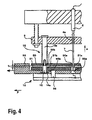
- Fig. 4 shows an embodiment in which the position of translator board 13 can be fine-adjusted relating to printed circuit board 19 to be inspected.
- a member corresponding to board 9 in Fig. 1 is composed of three boards 30, 31 and 32.
- Board 8 is formed with through-holes 8a respectively that receive test pin 7, as in the embodiment shown in Fig. 1.
- Board 30 is formed with through-holes 30a that respectively receive test pins 7, in the same manner as with board 8.
- Each test pin 7 is 0.4 mm in diameter, and each of through-holes 8a and 30a is 0.5 mm in diameter.
- Boards 31 and 32 are respectively formed with through-holes 31a and 32a, which are slightly larger in diameter than test pin 7.
- the diameter of test pin 7 is 0.4 mm, and that of through-holes 31a and 32a 0.8 mm.
- pin raiser 15 is provided between boards 8 and 30 to urge board 8 in the direction of the arrow ⁇ .
- Board 30 is formed with through-holes 30b.
- Boards 31 and 32 have through-holes 31b and 32b, respectively.
- Board 32 is formed with a spot facing of which a diameter is larger than that of head 16a of drop preventing screw 16.
- Drop preventing screw 16 is received by through-holes 31b and 32b, and the male screw of drop preventing screw 16 extends through through-holes 30b of board 30, and is screwed in pin raiser 15 to retain boards 31 and 32 on board 30.
- Through-holes 31b and 32b loosely receive drop preventing screw 16, and boards 31 and 32 are suspended with clearance t1 from board 30. In this condition, boards 31 and 32 can be moved relative to board 30. Pin raiser 15 retains board 30 not to move in the direction of arrow ⁇ relative to board 8.
- Positioning pin 35 retains translator board 13 and board 32 at positions.
- Board 32 is connected to a drive (not shown) and can move in the direction of the arrow ⁇ or in its opposite direction.
- test pin 7 has a diameter of 0.4 mm, and through-holes 31a and 32a have diameters of 0.8 mm. Thus, test pin 7 can move by 0.2 mm to the right or left.
- translator board 13 moves with board 32.
- test pin 7 is held vertical, as through-holes 31a and 32a are larger in diameter than test pin 7.
- test pin 7 can be held vertical by providing loose through-holes 9a at the same positions as these of through-holes 8a as shown in Fig. 1, and translator board 13 is employed for pitch conversion. Then, the embodiment enables two types of inspection, one of which employs translator board 13 as in the conventional universal type printed circuit board inspection apparatus 51, and the other of which uses test pin 7 without translator board 13.
- test pins 7 are held vertical extending through through-holes 8a and 30a. Accordingly, the embodiment is free from the problem that the tips of test pins 7 displace from inspection points when they engage a printed circuit board to be tested.
- test pins 7 are held vertical in this embodiment, they may be arranged to be held obliquely as in the conventional way, with pitches being reconverted by translator board 13.
- test pin 7 is not removed in this embodiment, an inspection using translator board can be done with a conventional printed circuit board inspection apparatus, without changing the shape of the tip of the probe (a dip).
- the position of translator board 13 can be adjusted, by slightly moving boards 31 and 32 horizontally (in X, Y, and ⁇ directions) with the board 32 being connected with a drive.
- Board 8 may also be connected with a drive to adjust the positions of boards 8, 30, 31 and 32. In this case, if at least through-holes 8a are made loose, displacement of probe 5 can be absorbed.
- Other through-holes, 30a, 31a and 32a may be either loose holes or fitting holes.
Landscapes
- Physics & Mathematics (AREA)
- General Physics & Mathematics (AREA)
- Testing Of Short-Circuits, Discontinuities, Leakage, Or Incorrect Line Connections (AREA)
- Measuring Leads Or Probes (AREA)
- Measurement Of Resistance Or Impedance (AREA)
Description
- The present invention relates to a printed circuit board inspecting apparatus, and particularly pertains to improvements of the versatility of a universal-type printed circuit board inspecting apparatus.
- Conventional universal-type printed circuit
board inspecting apparatus 51 as illustrated in Fig. 5, hasupper jig 2 andlower jig 3.Upper jig 2 hasbase 6 on which probes 5 are mounted in matrix arrangement. Board 8 is coupled withbase 6 through rods. Board 8 has through-holes 8a in the same position as that of probes 5. Board 8 is coupled withlower conversion board 49 throughpost 47.Lower conversion board 49 is formed with through-holes 49a at positions corresponding to the measuring points on the patterns printedcircuit board 19 which is to be inserted and put onlower jig 3.Test pins 7 are respectively inserted into through-holes 8a and 49a.Test pins 7 cooperate withboard 49 to convert the matrix arranged probe positions into actual measuring points. - Conductivity test is done in the following manner.
Lower jig 3 is raised by a lift (not illustrated), bringing each one end oftest pins 7 into contact with printedcircuit board 19 to be tested and the other ends oftest pins 7 are brought into contact with probes 5 inupper jig 2. The same happens to lowerjig 3. - In such conventional universal-type printed circuit
board inspection apparatus 51, any printed circuit board can be measured by replacinglower conversion board 49 with another one having through-holes 49a arranged according to the measuring points of printed circuit board to be inspected. - Nowadays, the pitches and spaces between printed circuit patterns become ever finer so that it is difficult to ensure accurate measurement with such conventional universal-type printed circuit
board inspecting apparatus 51 that employs exchangeable lower conversion board. - To cope with such problem, an inspection apparatus was proposed which employed a translator board instead of the test pins. (See Japanese patent application No. Showa54-129211.)
- However, the problems cited below occur when a translator board is mounted in space of test pins on such a conventional universal-type printed circuit board inspecting apparatus.
- Conductivity test is made with
lower jig 3 being raised by a lift (not illustrated). However, a given stroke is set for the movement oflower jig 3. Accordingly, if board 8,post 47 and conversionlower board 49 are removed from the universal-type printed circuitboard inspecting apparatus 51, the present stroke will be shorter than the stroke required for the inspection, disabling the operation of printed circuit board inspecting apparatus. - If the lifting range of the
lower jig 3 is changed to enable testing with the translator board to solve the above mentioned problem, inspections are possible only with a translator board. However, some inspections, such as those of relatively coarse-pitched printed circuit boards, are more easily done with the test pin system, because it is easier and cheaper to manufacturelower conversion boards 49 having through-holes 49a at given positions than to manufacture a translator board. - Moreover, when a printed circuit board that has been inspected, is reinspected, inspection is made with
lower conversion board 49, which has been stored and having through holes that meet the pattern of the inspected printed circuit board. In such reinspection,translator board 13 must be remade once the stroke of lifting the lower jig is adjusted. - Accordingly, DE 42 37591 A describes an inspecting apparatus for inspecting conductivity between and among inspection points on a printed circuit board, comprising a plurality of probes arranged in a predetermined pattern, a translator board including a first set of terminals arranged in the same pattern as that of the probes and a second set of terminals arranged in the same pattern as that of the inspection points on the printed circuit board to be inspected, the terminals of the first set being respectively electrically interconnected with corresponding terminals of the second set, the translator board being exchangeably mounted on the apparatus; and interconnecting pins for electrically interconnecting the probes with corresponding terminals of the first set of the translator board. An object of the present invention is to provide a printed circuit board inspecting apparatus which is capable of using either a pitch converting pin or pitch converting board in accordance with patterns or types of the printed circuit board to be tested.
- Accordingly an object of the present invention is to provide a printed circuit board inspection apparatus adapted for inspection of both fine and coarse pattern pitch printed circuit boards.
- Another object of the present invention is to provide a printed circuit board inspection apparatus in which a translator board for fine pitch board and a conversion board for coarse pitch board are alternatively used.
- Further object of the present invention is to provide a printed circuit board inspection apparatus wherein test pins for interconnecting probes and upper terminals of translator board are kept disengaged from the translator board while the apparatus is in rest condition.
- Still further object of the present invention is to provide a printed circuit board inspection apparatus wherein test pins for interconnecting probes and upper terminals of translator board are kept disengaged from the probes while the apparatus is in rest condition.
- According to the present invention, an inspecting apparatus for inspecting conductivity between and among inspection points on a printed circuit board, comprises a plurality of probes arranged in a predetermined pattern, a translator board including a first set of terminals arranged in the same pattern as that of the probes and a second set of terminals arranged in the same pattern as that of the inspection points on a printed circuit board to be inspected, the first set of terminals being respectively interconnected with corresponding terminals of the second set, the translator board being exchangeably mounted on the apparatus, and interconnecting pins for electrically interconnecting the probes with corresponding terminals of the first set of the translator board. This inspecting apparatus further comprises a supporting board for supporting the interconnecting pins and a biasing member for biasing the supporting board to keep off the tips of the interconnecting pins from the translator board while the apparatus is at rest.
- With the apparatus of the present invention, a conventional conversion board as shown in Figure 5 can be exchanged with the translator board and used without substantially changing the stroke of a lift that lifts the printed circuit board to the position to be inspected. The conversion board has through holes arranged to correspond to the inspection points on the printed circuit board and respectively receive the interconnecting pins such that the pins may be brought into contact with the inspection points.
- According to an embodiment of the present invention, a guide plate has a plurality of through-holed for guiding the interconnecting pins to the first set of terminals of the translator board. The guide plate may be coupled with the translator board with or without space therebetween. The set of the guide plate and the translator board may be exchanged with the conventional conversion board.
- According to the embodiment of the present invention, three plates work as the guide plate. First plate has a plurality of through holes each of which has a diameter substantially same as that of the interconnecting pin to receive the latter in smooth fitting manner. Second plate has a plurality of through holes each of which is slightly larger than that of the interconnecting pins for loose fitting with the pin, allowing slight displacement of the second plate relative-to the pins. Third plate is integrally coupled with the second plate and relative to the pins. Third plate is integrally coupled with the second plate and the translator board and is to be driven therewith to adjust them relative to the pins.
- According to the embodiment of the present invention, each tip of the interconnecting pins is loosely received by corresponding through-hole of the guide plate with a distance from the translator board while the apparatus is at rest.
- The above and other objects, features and advantages of the present invention will be apparent from the following detailed description of the preferred embodiments of the present invention in conjunction with the accompanying drawings, in which
- Fig. 1 is a partially cross-sectional schematic illustration of a printed circuit board inspection apparatus 1 as an embodiment of the present invention.
- Fig. 2 is cross-sections view of main portion of a translator board.
- Fig. 3 is a partially cross-sectional schematic illustration
of an embodiment using
translator lowerer 25. - Fig. 4 is a partially cross-section schematic illustration of another embodiment of the present invention which employs position adjusting mechanism.
- Fig. 5.is a partially cross-section schematic illustration of
conventional universal-type printed circuit
board inspection apparatus 51. -
- An embodiment of the present invention is described with reference to Fig. 1 which schematically illustrates a printed circuit board inspection apparatus 1 according to the present invention.
- Printed circuit board inspecting apparatus 1 has
upper jig 2 andlower jig 3.Upper jig 2 hasbase 6 on which probes 5 are mounted in matrix arrangement. Board 8 is coupled withbase 6 through a rod on whichspring 43 is wound around. Board 8 has through-holes 8a arranged in a matrix andboard 9 also has through-holes 9a, which are at the same positions as those of through-holes 8.Test pins 7 extend through through-holes 8a and 49a. In the present embodiment,test pin 7 has a diameter of 0.4 mm, and through-holes 8a and 9a have respectively a diameter of 0.5 mm. Heads 7a oftest pins 7 are retained on the upper side of board 8. -
Pin raiser 15 is interposed betweenboards 8 and 9.Pin raiser 15 is composed ofbody 15a andspring 15b.Spring 15b urges the board 8 in the direction of the arrow α to move away fromboard 9. Thus, head 7a oftest pin 7 is lifted in the direction of the arrow α, withtip 7b oftest pin 7 being kept from contacting the upper surface oftranslator board 13 through clearance t0.Translator board 13 is fixed toboard 9 withscrews 21. - Next, description is about
translator board 13, with reference to Fig. 2. The translator board is used for inspection of printed circuit boards of electric conductor patterns with pitches finer than those between the probes of a universal-type jig. Thetranslator board 13 includesinspection electrodes 11c arranged to match the electric conductor pattern of a printed circuit board to be inspected.Translator board 13 includesconverter 11 and electricallyconductive rubber portion 12.Converter 11 is provided withelectrodes 11a on the probe side andelectrodes 11c on the inspection side.Electrode 11c on the inspection side is provided with electricallyconductive rubber portion 12. Electricallyconductive rubber portion 12 is equipped with non uniformly arrangedPCR part 12r. The "Offgrid Adapter JP2000" manufactured by JSR Nippon Synthetic Rubber Co., Ltd. is used astranslator board 13 in the present embodiment. - Printed
circuit board 19 to be inspected is put onlower jig 3 in the conventional way. With the structure as mentioned above,pin raiser 15 betweenboards 8 and 9 preventstip 7b from coming into contact with the measuring point oftranslator board 13 when no inspection occurs. At the time, the weight oftest pin 7 is kept fromtranslator board 13, preventing warping or damage oftranslator board 13. - Through-holes 8a and 9a are designed to be slightly broader in diameter than test pins 7. Pitches are converted by
translator board 13, andtest pins 7 can be held almost vertical, avoiding the problem that tips of the test pinscontact translator board 13 at points displaced from predetermined position. - In the above mentioned embodiment,
pin raiser 15 pulls up board 8 in the direction of the arrow α fromboard 9. It is possible thattranslator lowering member 25 urgestranslator board 13 in the direction opposite to the arrow α, as shown in Fig. 3. Within its body 25a,translator lowering member 25 incorporates a spring (not illustrated), which urgestranslator board 13 to move away fromboard 9. - Explanation will then be made about another embodiment with reference to Fig. 4, which shows an embodiment in which the position of
translator board 13 can be fine-adjusted relating to printedcircuit board 19 to be inspected. - In this embodiment, a member corresponding to
board 9 in Fig. 1 is composed of threeboards test pin 7, as in the embodiment shown in Fig. 1.Board 30 is formed with through-holes 30a that respectively receivetest pins 7, in the same manner as with board 8. Eachtest pin 7 is 0.4 mm in diameter, and each of through-holes 8a and 30a is 0.5 mm in diameter. -
Boards holes 31a and 32a, which are slightly larger in diameter thantest pin 7. In the present embodiment, the diameter oftest pin 7 is 0.4 mm, and that of through-holes 31a and 32a 0.8 mm. - As in the embodiment shown Fig. 1,
pin raiser 15 is provided betweenboards 8 and 30 to urge board 8 in the direction of the arrow α.Board 30 is formed with through-holes 30b.Boards holes 31b and 32b, respectively.Board 32 is formed with a spot facing of which a diameter is larger than that ofhead 16a ofdrop preventing screw 16. Drop preventingscrew 16 is received by through-holes 31b and 32b, and the male screw ofdrop preventing screw 16 extends through through-holes 30b ofboard 30, and is screwed inpin raiser 15 to retainboards board 30. - Through-
holes 31b and 32b loosely receivedrop preventing screw 16, andboards board 30. In this condition,boards board 30.Pin raiser 15 retainsboard 30 not to move in the direction of arrow β relative to board 8. - Positioning pin 35 retains
translator board 13 andboard 32 at positions.
Board 32 is connected to a drive (not shown) and can move in the direction of the arrow β or in its opposite direction. In this embodiment mentioned above,test pin 7 has a diameter of 0.4 mm, and through-holes 31a and 32a have diameters of 0.8 mm. Thus,test pin 7 can move by 0.2 mm to the right or left. - When the drive (not shown) moves
board 32 in the direction of arrow β or oppositely,translator board 13 moves withboard 32. In this case,test pin 7 is held vertical, as through-holes 31a and 32a are larger in diameter thantest pin 7. Thus, without moving the entire upper jig,translator board 13 is easily positioned relative to printedcircuit board 19 to be inspected. - Further the tips of
test pins 7 are kept off from the patterns oftranslator board 13 in this embodiment so that the pattern will not be damaged whentranslator board 13 moves horizontally. Thus, instead of providinglower conversion board 49 as shown in Fig. 5,test pin 7 can be held vertical by providing loose through-holes 9a at the same positions as these of through-holes 8a as shown in Fig. 1, andtranslator board 13 is employed for pitch conversion. Then, the embodiment enables two types of inspection, one of which employstranslator board 13 as in the conventional universal type printed circuitboard inspection apparatus 51, and the other of which usestest pin 7 withouttranslator board 13. - In the present embodiment,
test pins 7 are held vertical extending through through-holes 8a and 30a. Accordingly, the embodiment is free from the problem that the tips oftest pins 7 displace from inspection points when they engage a printed circuit board to be tested. - Although
test pins 7 are held vertical in this embodiment, they may be arranged to be held obliquely as in the conventional way, with pitches being reconverted bytranslator board 13. - As
test pin 7 is not removed in this embodiment, an inspection using translator board can be done with a conventional printed circuit board inspection apparatus, without changing the shape of the tip of the probe (a dip). - In the present embodiment, the position of
translator board 13 can be adjusted, by slightly movingboards board 32 being connected with a drive. Board 8 may also be connected with a drive to adjust the positions ofboards - While the invention has been particularly shown and described with reference to preferred embodiments thereof, it will be understood by those skilled in the art that the foregoing and other changes in form and details can be made therein without departing from the scope of the invention.
Claims (4)
- An inspecting apparatus for inspecting conductivity between and among inspection points on a printed circuit board, said apparatus comprising:characterized by:a plurality of probes (5) arranged in a predetermined pattern;a translator board (13) including a first set of terminals (11a) arranged in the same pattern as that of the probes and a second set of terminals (11c) arranged in the same pattern as that of the inspection points on a printed circuit board to be inspected, the first set of terminals (11a) being respectively electrically interconnected with corresponding terminals of the second set (11c), the translator board (13) being exchangeably mounted on the apparatus; andinterconnecting pins (7) for electrically interconnecting the probes (5) with corresponding terminals (11a) of the first set of the translator board;
a supporting board (8) for supporting the interconnecting pins (7) and a biasing member (15b) for biasing the supporting board (8) to keep off the tips (7b) of the interconnecting pins (7) from the translator board (13) while the apparatus is at rest. - A printed circuit board inspecting apparatus according to Claim 1, further comprising a guide plate (9) including a plurality of through-holes (9a) for guiding the interconnecting pins (7) to the first set of terminals (11a) of the translator board (13), said guide plate (9) being integrally coupled with the translator board (13).
- A printed circuit board inspecting apparatus according to Claim 1, further comprising a first plate (30) having a plurality of through-holes (30a), each of which having a diameter substantially the same as that of the interconnecting pin (7) to receive the latter in smooth fitting manner; a second plate (31) having a plurality of through-holes (31a) each of which is slightly larger than that of the interconnecting pins (7) for loose fitting with the pins (7), allowing slight displacement of the second plate (31) relative to the pins (7); a third plate (32) integrally coupled with the second plate (31) and the translator board (13) and a driving member for adjusting the second and third plates (31, 32) and the translator board (13) relative to the pins (7).
- A printed circuit board inspecting apparatus according to any one of Claims 1 to 3, wherein said predetermined pattern is a matrix and the supporting board (8) includes a plurality of through-holes (8a) arranged in said matrix, each of the interconnecting pins (7) having an enlarged head (7a) so as to be held on an upper side of the supporting board and wherein a diameter of each through-hole (8a) is larger than a diameter of the respective interconnecting pin (7) passing therethrough.
Applications Claiming Priority (3)
| Application Number | Priority Date | Filing Date | Title |
|---|---|---|---|
| JP32563796 | 1996-12-05 | ||
| JP08325637A JP3099873B2 (en) | 1996-12-05 | 1996-12-05 | Method of using printed board inspection apparatus and universal type printed board inspection apparatus |
| JP325637/96 | 1996-12-05 |
Publications (3)
| Publication Number | Publication Date |
|---|---|
| EP0846953A2 EP0846953A2 (en) | 1998-06-10 |
| EP0846953A3 EP0846953A3 (en) | 1998-08-19 |
| EP0846953B1 true EP0846953B1 (en) | 2001-10-24 |
Family
ID=18179070
Family Applications (1)
| Application Number | Title | Priority Date | Filing Date |
|---|---|---|---|
| EP97121442A Expired - Lifetime EP0846953B1 (en) | 1996-12-05 | 1997-12-05 | Printed circuit board inspecting apparatus |
Country Status (4)
| Country | Link |
|---|---|
| US (1) | US6049214A (en) |
| EP (1) | EP0846953B1 (en) |
| JP (1) | JP3099873B2 (en) |
| DE (1) | DE69707624T2 (en) |
Families Citing this family (9)
| Publication number | Priority date | Publication date | Assignee | Title |
|---|---|---|---|---|
| US20020053734A1 (en) | 1993-11-16 | 2002-05-09 | Formfactor, Inc. | Probe card assembly and kit, and methods of making same |
| US6483328B1 (en) | 1995-11-09 | 2002-11-19 | Formfactor, Inc. | Probe card for probing wafers with raised contact elements |
| US6447339B1 (en) * | 2001-12-12 | 2002-09-10 | Tektronix, Inc. | Adapter for a multi-channel signal probe |
| US6876211B2 (en) * | 2002-03-13 | 2005-04-05 | Seagate Technology Llc | Printed circuit board test fixture that supports a PCB to be tested |
| CN100592432C (en) * | 2006-11-16 | 2010-02-24 | 鸿富锦精密工业(深圳)有限公司 | Mainboard fixing device |
| TWI439709B (en) * | 2006-12-29 | 2014-06-01 | Intest Corp | Manupulator and load positioning system for translating load along axis of translation |
| US8350584B2 (en) * | 2006-12-29 | 2013-01-08 | Intest Corporation | Test head positioning system and method |
| JP2013015508A (en) * | 2011-06-06 | 2013-01-24 | Ricoh Co Ltd | Substrate inspection jig and substrate inspection method |
| US11050208B2 (en) * | 2018-10-31 | 2021-06-29 | International Business Machines Corporation | Pre-screening, compliant pin guiding and quality monitoring press-fit apparatus |
Family Cites Families (10)
| Publication number | Priority date | Publication date | Assignee | Title |
|---|---|---|---|---|
| US3654585A (en) * | 1970-03-11 | 1972-04-04 | Brooks Research And Mfg Inc | Coordinate conversion for the testing of printed circuit boards |
| US4551675A (en) * | 1983-12-19 | 1985-11-05 | Ncr Corporation | Apparatus for testing printed circuit boards |
| US4724383A (en) * | 1985-05-03 | 1988-02-09 | Testsystems, Inc. | PC board test fixture |
| FR2634025B1 (en) * | 1988-07-08 | 1990-11-09 | Thomson Csf | PINING ADAPTER FOR TESTING HIGH DENSITY PRINTED CIRCUITS |
| US5399982A (en) * | 1989-11-13 | 1995-03-21 | Mania Gmbh & Co. | Printed circuit board testing device with foil adapter |
| DE4237591A1 (en) * | 1992-11-06 | 1994-05-11 | Mania Gmbh | PCB test facility with foil adapter |
| KR100288344B1 (en) * | 1991-09-17 | 2001-11-30 | 마쯔모또 에이찌 | Inspection electrode unit for printed wiring boards, inspection apparatus including the same, and inspection method for printed wiring boards |
| DE19507127A1 (en) * | 1995-03-01 | 1996-09-12 | Test Plus Electronic Gmbh | Adapter system for component boards, to be used in a test facility |
| US5883520A (en) * | 1996-06-14 | 1999-03-16 | Star Technology Group, Inc. | Retention of test probes in translator fixtures |
| US5828226A (en) * | 1996-11-06 | 1998-10-27 | Cerprobe Corporation | Probe card assembly for high density integrated circuits |
-
1996
- 1996-12-05 JP JP08325637A patent/JP3099873B2/en not_active Expired - Fee Related
-
1997
- 1997-12-05 US US08/985,848 patent/US6049214A/en not_active Expired - Fee Related
- 1997-12-05 DE DE69707624T patent/DE69707624T2/en not_active Expired - Fee Related
- 1997-12-05 EP EP97121442A patent/EP0846953B1/en not_active Expired - Lifetime
Also Published As
| Publication number | Publication date |
|---|---|
| EP0846953A2 (en) | 1998-06-10 |
| US6049214A (en) | 2000-04-11 |
| JP3099873B2 (en) | 2000-10-16 |
| EP0846953A3 (en) | 1998-08-19 |
| DE69707624D1 (en) | 2001-11-29 |
| DE69707624T2 (en) | 2002-07-18 |
| JPH10170580A (en) | 1998-06-26 |
Similar Documents
| Publication | Publication Date | Title |
|---|---|---|
| KR100343252B1 (en) | Connection method for inspection equipment and inspection equipment | |
| KR100213840B1 (en) | Semiconductor tester | |
| EP0846953A2 (en) | Printed circuit board inspecting apparatus, and method of using a universal-type printed circuit board inspecting apparatus | |
| JP2007256277A (en) | Apparatus for scan testing printed circuit board | |
| US8120375B2 (en) | Method for using probe card | |
| KR100995811B1 (en) | Probe unit for fine positioning of the probe | |
| CN1175270C (en) | Machines for electrical testing of printed circuits with adjustable probe positions | |
| US4834659A (en) | Adaptor in apparatus for electronically testing printed circuit boards | |
| KR101388989B1 (en) | Jig for substrate inspection, base units of jig and substrate inspection apparatus | |
| KR0155573B1 (en) | Inspection device of semiconductor device | |
| KR102236995B1 (en) | Eddy current test device | |
| JP3014055B2 (en) | Electrical check device for printed wiring boards | |
| CN115032428B (en) | A plug-in single board test device | |
| KR20070117452A (en) | Board inspection fixture and board inspection device | |
| KR20180125340A (en) | Contactor clamping device for display panel pallet | |
| CN224152598U (en) | A static fixture for a semiconductor power module | |
| CN223808227U (en) | Bending-resistant dynamic and static test device for insulating operating rod | |
| CN219292956U (en) | Flat cable welding positioning jig | |
| CN221148855U (en) | Portable testing mold for FPC flexible circuit board | |
| JPH0213861A (en) | Fixture of printed circuit board wiring tester | |
| JPS6161560B2 (en) | ||
| KR20000000251U (en) | Pitch adjusting device of pickup head for semiconductor handler | |
| JPH0438299Y2 (en) | ||
| KR20050067760A (en) | A semiconductor test device | |
| JPH045025Y2 (en) |
Legal Events
| Date | Code | Title | Description |
|---|---|---|---|
| PUAI | Public reference made under article 153(3) epc to a published international application that has entered the european phase |
Free format text: ORIGINAL CODE: 0009012 |
|
| AK | Designated contracting states |
Kind code of ref document: A2 Designated state(s): DE FR GB |
|
| AX | Request for extension of the european patent |
Free format text: AL;LT;LV;MK;RO;SI |
|
| PUAL | Search report despatched |
Free format text: ORIGINAL CODE: 0009013 |
|
| AK | Designated contracting states |
Kind code of ref document: A3 Designated state(s): AT BE CH DE DK ES FI FR GB GR IE IT LI LU MC NL PT SE |
|
| AX | Request for extension of the european patent |
Free format text: AL;LT;LV;MK;RO;SI |
|
| 17P | Request for examination filed |
Effective date: 19980921 |
|
| AKX | Designation fees paid |
Free format text: DE FR GB |
|
| RBV | Designated contracting states (corrected) |
Designated state(s): DE FR GB |
|
| 17Q | First examination report despatched |
Effective date: 19991129 |
|
| RTI1 | Title (correction) |
Free format text: PRINTED CIRCUIT BOARD INSPECTING APPARATUS |
|
| GRAG | Despatch of communication of intention to grant |
Free format text: ORIGINAL CODE: EPIDOS AGRA |
|
| RIN1 | Information on inventor provided before grant (corrected) |
Inventor name: MIKI, TAKASHI,NIDEC-READ CORP. Inventor name: NISHIKAWA, HIDEO |
|
| GRAG | Despatch of communication of intention to grant |
Free format text: ORIGINAL CODE: EPIDOS AGRA |
|
| GRAH | Despatch of communication of intention to grant a patent |
Free format text: ORIGINAL CODE: EPIDOS IGRA |
|
| GRAH | Despatch of communication of intention to grant a patent |
Free format text: ORIGINAL CODE: EPIDOS IGRA |
|
| GRAA | (expected) grant |
Free format text: ORIGINAL CODE: 0009210 |
|
| AK | Designated contracting states |
Kind code of ref document: B1 Designated state(s): DE FR GB |
|
| REF | Corresponds to: |
Ref document number: 69707624 Country of ref document: DE Date of ref document: 20011129 |
|
| REG | Reference to a national code |
Ref country code: GB Ref legal event code: IF02 |
|
| ET | Fr: translation filed | ||
| PLBE | No opposition filed within time limit |
Free format text: ORIGINAL CODE: 0009261 |
|
| STAA | Information on the status of an ep patent application or granted ep patent |
Free format text: STATUS: NO OPPOSITION FILED WITHIN TIME LIMIT |
|
| 26N | No opposition filed | ||
| PGFP | Annual fee paid to national office [announced via postgrant information from national office to epo] |
Ref country code: GB Payment date: 20021210 Year of fee payment: 6 |
|
| PGFP | Annual fee paid to national office [announced via postgrant information from national office to epo] |
Ref country code: FR Payment date: 20030214 Year of fee payment: 6 |
|
| PGFP | Annual fee paid to national office [announced via postgrant information from national office to epo] |
Ref country code: DE Payment date: 20030328 Year of fee payment: 6 |
|
| PG25 | Lapsed in a contracting state [announced via postgrant information from national office to epo] |
Ref country code: GB Free format text: LAPSE BECAUSE OF NON-PAYMENT OF DUE FEES Effective date: 20031205 |
|
| PG25 | Lapsed in a contracting state [announced via postgrant information from national office to epo] |
Ref country code: DE Free format text: LAPSE BECAUSE OF NON-PAYMENT OF DUE FEES Effective date: 20040701 |
|
| GBPC | Gb: european patent ceased through non-payment of renewal fee |
Effective date: 20031205 |
|
| PG25 | Lapsed in a contracting state [announced via postgrant information from national office to epo] |
Ref country code: FR Free format text: LAPSE BECAUSE OF NON-PAYMENT OF DUE FEES Effective date: 20040831 |
|
| REG | Reference to a national code |
Ref country code: FR Ref legal event code: ST |