EP0846273B1 - Dispositif d'interface radiofrequence pour transpondeur - Google Patents
Dispositif d'interface radiofrequence pour transpondeur Download PDFInfo
- Publication number
- EP0846273B1 EP0846273B1 EP96922729A EP96922729A EP0846273B1 EP 0846273 B1 EP0846273 B1 EP 0846273B1 EP 96922729 A EP96922729 A EP 96922729A EP 96922729 A EP96922729 A EP 96922729A EP 0846273 B1 EP0846273 B1 EP 0846273B1
- Authority
- EP
- European Patent Office
- Prior art keywords
- transponder
- coil
- terminals
- voltage
- interface
- Prior art date
- Legal status (The legal status is an assumption and is not a legal conclusion. Google has not performed a legal analysis and makes no representation as to the accuracy of the status listed.)
- Expired - Lifetime
Links
Images


Classifications
-
- G—PHYSICS
- G01—MEASURING; TESTING
- G01S—RADIO DIRECTION-FINDING; RADIO NAVIGATION; DETERMINING DISTANCE OR VELOCITY BY USE OF RADIO WAVES; LOCATING OR PRESENCE-DETECTING BY USE OF THE REFLECTION OR RERADIATION OF RADIO WAVES; ANALOGOUS ARRANGEMENTS USING OTHER WAVES
- G01S13/00—Systems using the reflection or reradiation of radio waves, e.g. radar systems; Analogous systems using reflection or reradiation of waves whose nature or wavelength is irrelevant or unspecified
- G01S13/02—Systems using reflection of radio waves, e.g. primary radar systems; Analogous systems
-
- G—PHYSICS
- G06—COMPUTING OR CALCULATING; COUNTING
- G06K—GRAPHICAL DATA READING; PRESENTATION OF DATA; RECORD CARRIERS; HANDLING RECORD CARRIERS
- G06K19/00—Record carriers for use with machines and with at least a part designed to carry digital markings
- G06K19/06—Record carriers for use with machines and with at least a part designed to carry digital markings characterised by the kind of the digital marking, e.g. shape, nature, code
- G06K19/067—Record carriers with conductive marks, printed circuits or semiconductor circuit elements, e.g. credit or identity cards also with resonating or responding marks without active components
- G06K19/07—Record carriers with conductive marks, printed circuits or semiconductor circuit elements, e.g. credit or identity cards also with resonating or responding marks without active components with integrated circuit chips
- G06K19/0701—Record carriers with conductive marks, printed circuits or semiconductor circuit elements, e.g. credit or identity cards also with resonating or responding marks without active components with integrated circuit chips at least one of the integrated circuit chips comprising an arrangement for power management
-
- G—PHYSICS
- G01—MEASURING; TESTING
- G01S—RADIO DIRECTION-FINDING; RADIO NAVIGATION; DETERMINING DISTANCE OR VELOCITY BY USE OF RADIO WAVES; LOCATING OR PRESENCE-DETECTING BY USE OF THE REFLECTION OR RERADIATION OF RADIO WAVES; ANALOGOUS ARRANGEMENTS USING OTHER WAVES
- G01S13/00—Systems using the reflection or reradiation of radio waves, e.g. radar systems; Analogous systems using reflection or reradiation of waves whose nature or wavelength is irrelevant or unspecified
- G01S13/74—Systems using reradiation of radio waves, e.g. secondary radar systems; Analogous systems
- G01S13/75—Systems using reradiation of radio waves, e.g. secondary radar systems; Analogous systems using transponders powered from received waves, e.g. using passive transponders, or using passive reflectors
- G01S13/751—Systems using reradiation of radio waves, e.g. secondary radar systems; Analogous systems using transponders powered from received waves, e.g. using passive transponders, or using passive reflectors wherein the responder or reflector radiates a coded signal
- G01S13/758—Systems using reradiation of radio waves, e.g. secondary radar systems; Analogous systems using transponders powered from received waves, e.g. using passive transponders, or using passive reflectors wherein the responder or reflector radiates a coded signal using a signal generator powered by the interrogation signal
-
- G—PHYSICS
- G06—COMPUTING OR CALCULATING; COUNTING
- G06K—GRAPHICAL DATA READING; PRESENTATION OF DATA; RECORD CARRIERS; HANDLING RECORD CARRIERS
- G06K7/00—Methods or arrangements for sensing record carriers, e.g. for reading patterns
- G06K7/0008—General problems related to the reading of electronic memory record carriers, independent of its reading method, e.g. power transfer
-
- H—ELECTRICITY
- H02—GENERATION; CONVERSION OR DISTRIBUTION OF ELECTRIC POWER
- H02M—APPARATUS FOR CONVERSION BETWEEN AC AND AC, BETWEEN AC AND DC, OR BETWEEN DC AND DC, AND FOR USE WITH MAINS OR SIMILAR POWER SUPPLY SYSTEMS; CONVERSION OF DC OR AC INPUT POWER INTO SURGE OUTPUT POWER; CONTROL OR REGULATION THEREOF
- H02M7/00—Conversion of AC power input into DC power output; Conversion of DC power input into AC power output
- H02M7/02—Conversion of AC power input into DC power output without possibility of reversal
- H02M7/04—Conversion of AC power input into DC power output without possibility of reversal by static converters
- H02M7/06—Conversion of AC power input into DC power output without possibility of reversal by static converters using discharge tubes without control electrode or semiconductor devices without control electrode
- H02M7/10—Conversion of AC power input into DC power output without possibility of reversal by static converters using discharge tubes without control electrode or semiconductor devices without control electrode arranged for operation in series, e.g. for multiplication of voltage
-
- H—ELECTRICITY
- H02—GENERATION; CONVERSION OR DISTRIBUTION OF ELECTRIC POWER
- H02M—APPARATUS FOR CONVERSION BETWEEN AC AND AC, BETWEEN AC AND DC, OR BETWEEN DC AND DC, AND FOR USE WITH MAINS OR SIMILAR POWER SUPPLY SYSTEMS; CONVERSION OF DC OR AC INPUT POWER INTO SURGE OUTPUT POWER; CONTROL OR REGULATION THEREOF
- H02M7/00—Conversion of AC power input into DC power output; Conversion of DC power input into AC power output
- H02M7/02—Conversion of AC power input into DC power output without possibility of reversal
- H02M7/04—Conversion of AC power input into DC power output without possibility of reversal by static converters
- H02M7/06—Conversion of AC power input into DC power output without possibility of reversal by static converters using discharge tubes without control electrode or semiconductor devices without control electrode
- H02M7/10—Conversion of AC power input into DC power output without possibility of reversal by static converters using discharge tubes without control electrode or semiconductor devices without control electrode arranged for operation in series, e.g. for multiplication of voltage
- H02M7/103—Containing passive elements (capacitively coupled) which are ordered in cascade on one source
Definitions
- the present invention relates to the interface radio frequency of a transponder, and in particular the circuit voltage converter of such an interface.
- the invention applies in particular to the interface radio frequency of a transponder used as a device contactless identification.
- Devices of this type include an antenna electromagnetic in the form of an inductive coil of very small dimensions, connected in input / output to a integrated circuit through a converter circuit voltage, providing the DC supply voltage of the integrated circuit.
- Transponders of this type do not have battery and are intended to exchange data with a interrogation or identification device to which they are not connected by a wired connection. Voltage power the transponder needs to operate is therefore obtained from a radio frequency excitation signal emitted by the device question mark. This radio frequency signal is rectified in the transponder and the voltage thus produced is used to charge a capacitor constituting a means energy storage. The energy thus stored is used by transponder circuits to write to it information in logic circuits, including memories, and to modulate a radio frequency signal from response intended for the reading of the transponder by the interrogation device.
- transponder device Such a transponder device is described in the US document A-4,196,418.
- This device includes effect a rectifier circuit for rectifying and therefore to use the voltage of the resonator circuit for supply the various components of the device.
- transponders can in practice be used in a wide variety of applications, including for remote object identification.
- one of the problems posed lies in the fact that the input voltage of the interface of the transponder determines the limit distance of operation, i.e. maximum distance acceptable between transmitter or receiver of a signal electromagnetic and the transponder to allow data exchange between the source and the transponder. Therefore, to increase the operating distance, it is known in the prior art to use a voltage doubler at the output of the rectifier circuit, but in this case, the rectifier diodes of the interface risk of cracking due to excessive tension reverse caused by this doubler.
- the object of the present invention is to remedy these disadvantages, and to propose an interface device able to increase the operating distance while preventing a large reverse voltage from being applied to the rectifier diodes of the interface. Moreover, the invention aims to provide a device allowing the incorporation of standard circuits of protection, which is not possible with a doubler of classic tension.
- Another object of the invention is to propose a transponder interface capable of generating current sufficient for the transponder to receive a microprocessor or other integrated circuits having a relatively high current consumption, especially non-volatile memory.
- the invention relates to an interface transponder radio frequency, comprising a coil forming the transponder antenna and a circuit voltage converter connected on the one hand to the terminals of said coil and on the other hand to the power supply terminals DC voltage of an integrated logic circuit of the transponder, characterized in that the terminals of the coil are connected to floating potentials by relative to the transponder substrate, so that the potential of none of the coil terminals goes below of the potential of the substrate, and in that said voltage converter is a voltage tripler which comprises a first rectifier connected to the terminals of the coil and constituted by a first diode in series with a first capacitor, a second rectifier connected to terminals of the first diode and constituted by a second diode in series with a second capacitor, and a third rectifier connected between the terminals of the first capacitor and constituted by a third diode in series with a third capacitor.
- the invention also relates to a device transponder comprising an interface device having any of the foregoing features.
- FIG. 1 We have represented in this figure a block diagram showing the main functional blocks of a transponder, and particular of its radiofrequency interface 1.
- a transponder has an antenna in the form of a coil 2 of small dimensions, preferably connected in parallel to a capacitor 3, and to the entry of a stage voltage converter 4 which transforms the alternative input voltage available at terminals 5.6 coil 2, in direct voltage (Vdd-Vss) allowing to supply a block of logic circuits 7 of the transponder, consisting for example of a memory or a microprocessor.
- the input signal available at the terminals of coil 2 is also demodulated, in the direction of writing, by a demodulation block 8 for writing data information to the integrated circuits 7 of the transponder.
- the data intended for be read from the transponder are modulated by a modulation block 9 supplying the coil 2 for the reading of data from the transponder by a contactless identification device (not shown).
- the write signal to the transponder is used by a clock recovery block 10 used to generate a clock signal for logic circuits 7 of the transponder, synchronous signal of the external recognition device.
- the invention relates more particularly to voltage converter 4 of radio frequency interface 1 of the transponder.
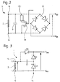
- Figure 2 represents a diagram of the input / output interface according to the state of the technique, in which identical elements or similar to those in figure 1 are assigned a number identical reference.
- the diagram in Figure 2 makes call to a Gräetz 11 bridge connected to the terminals 5.6 of coil 2, and generating a voltage output continues Vdd-Vss.
- a transistor 12 used to modulate the radiofrequency field in modulating coil current 2 using the information binaries to be read from the transponder, which are brought on the gate G of the transistor.
- the transistor 12 is connected in series with a resistor 13.
- Interface assembly 1 at the Gräetz 11 bridge is not not very effective for highly resistive loads.
- the output voltage (Vdd-Vss) of the bridge is at least one diode voltage drop (0.7V) to the amplitude of the input voltage of the coil 2.
- the modulation transistor 12 is highly resistive in weak fields. Therefore it it is not recommended to add a resistor 13 in series with transistor 12. It follows that the resistance of modulation in weak fields is high, which causes a slow decrease in the current of the coil 2 and can thus cause false clock pulses. This effect becomes even more critical since the modulation takes place only during half a wave of the coil voltage. This results in a shift of the point of operation of the clock extraction circuit 10.
- Figure 3 representing another input / output interface diagram according to the state of the technique, which uses a rectifier stage 14 with a doubler voltage, a terminal 6 of the coil 2 being connected to the substrate of the transponder's logic circuits.
- the voltage doubler 14 is more effective for the weak coil voltages as the assembly of Figure 2, so that the problems with modulation are less apparent, the operating distance being greater due to the higher modulation voltage.
- diode D3 must be added in order to generate the high current required during writing. This diode is exposed to a relatively reverse voltage high, about three times the magnitude of the voltage coil input, when the voltage doubler 14 is connected to a low load (not shown). This is a significant disadvantage for designs to based on poly-diodes, which have voltages of relatively weak breakdown.
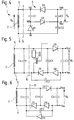
- a radiofrequency interface 1 according to the invention is shown schematically in Figure 4.
- the interface 1 includes a coil 2 and a voltage converter 4 delimited by the broken line 15.
- the converter 4 is mounted as a voltage multiplier, plus precisely as a voltage tripler in the example represented, without this example having a character limiting, since other multiplication ratios of voltage can be retained by the skilled person in according to the specific needs of the application considered.
- the voltage converter 4 includes a first rectifier (D1, C1) which charges the capacitor C1 under a voltage amplitude equal to the amplitude of the input voltage.
- the rectifier stage (D1, C1) is followed by a second stage rectifier (D2, C2) which again rectifies the voltage of output of the first rectifier, so that the voltage of second rectifier output across capacitor C2 is now of double the amplitude of the voltage input Ve.
- Signals input Ve and output Vs are shown respectively in Figures 7 and 8.
- the input voltage a radio frequency transponder interface has general an amplitude between 1 and 20 Volts and a frequency of the order of 125 kHz to a few MHz, and the amplitude of the DC output voltage sought is in the range of 1 to 5 Volts.
- the input voltage has in the example shown an amplitude of the order of 1.3 Volts.
- the mounting of the converter voltage 4 is made so that the terminals 5,6 of the coil 2 are at floating potential with respect to potential of the Vss substrate. So unlike the mounting of the state of the art ( Figure 2), none of the terminals 5,6 of the coil 2 do not pass under the potential Vss, so that none of the diodes of the rectifier stages is exposed to a reverse voltage of amplitude greater than double the amplitude of the input voltage, so that breakdown voltages of the diodes of the rectifier stages less likely to be affected even when used of poly-diodes.
- FIG. 5 represents a variant of the interface 1 of Figure 4, in which the modulation transistor 12 of the voltage converter, as well as a resistor 13 connected in series with it.
- This very simple modulation arrangement is possible from fact that during normal operation of the interface 1, none of the terminals 5,6 of the coil 2 has a potential located outside the range between Vss-0.7 V and Vdd + 0.7 V.
- the modulation transistor 12 has a resistance to the lower passing state, so that a resistance 13 can be used to achieve a rapid decrease in coil current 2 under all conditions operation.
- This rapid decrease results in a easily detectable signal in the reading device outside, while reducing the risk of signals clock errors in interface 1, since it remains always a sufficient voltage amplitude between the terminals 5.6 of the coil to extract the clock signal in good conditions.
- a capacitor C4 connected to the terminals of the coil 2, so as to form between the coil and the capacitor C4 a resonant circuit with the same frequency as that of the electromagnetic field, making it possible to improve the coupling factor and therefore use less energy for the transmission of information between the transponder and the external reading device.
- the polarity of diodes D1, D2, D3 is reversed compared to that corresponding to FIG. 4, this inversion being due to p-type junction technology rather than type n.
- Figure 6 relates to an additional variant of the interface according to the invention, in which the modulation transistor 12 has not been shown at for the sake of simplicity.
- the stray diode D4 is taken into account present on the substrate between coil 2 and the output of interface 1.
- this diode D4 is used as a single-wave rectifier, allowing reduce the voltage drop by 0.7 Volt during writing to the transducer. Indeed, in this case, at instead of having D1, D2, D3 connected in series, there remains only D3 and D4, so that the DC output voltage Vs is even higher than in the case of FIG. 5.
- the substrate diodes, of the D4 type have higher breakdown voltages than poly-diodes which are floating relative to the substrate of the transponder, there is no risk of breakdown.
- the interface radio frequency according to the invention perfectly fulfills the goals set. It allows you to combine the advantages of known montages with Gräetz bridge and doubler, while avoiding their disadvantages.
- none of the interface rectifier stage diodes are not exposed at a reverse voltage greater than twice the voltage across the input / output coil. Therefore the risk of breakdown is less than it is in the case of a voltage doubler interface, even in using poly-diodes.
- the DC output voltage is more high, for the same input voltage at the coil.
- the operating distance of the transponder is increased in large proportions to go from a few centimeters to several meters.
- the transponder may include a microprocessor.
Landscapes
- Engineering & Computer Science (AREA)
- Radar, Positioning & Navigation (AREA)
- Remote Sensing (AREA)
- Physics & Mathematics (AREA)
- General Physics & Mathematics (AREA)
- Theoretical Computer Science (AREA)
- Microelectronics & Electronic Packaging (AREA)
- Computer Hardware Design (AREA)
- Computer Networks & Wireless Communication (AREA)
- Power Engineering (AREA)
- Computer Vision & Pattern Recognition (AREA)
- Artificial Intelligence (AREA)
- Near-Field Transmission Systems (AREA)
- Radar Systems Or Details Thereof (AREA)
- Burglar Alarm Systems (AREA)
Description
- l'interface comporte un transistor de modulation dont le drain et la source sont connectés entre les bornes de la bobine, et dont la grille est alimentée par un signal de modulation issu du circuit intégré du transpondeur.
- ledit transistor de modulation est connecté en série avec une résistance, de sorte que le courant de la bobine varie rapidement de façon à moduler le champ radiofréquence.
- avantageusement, une diode de substrat est connectée entre une borne de la bobine et le substrat du transpondeur, en parallèle auxdites premières et secondes diodes, de façon à diminuer la chute de tension d'écriture de l'ordre de 0,7V.
- de préférence un condensateur est connecté aux bornes de la bobine, de façon à former un circuit résonant améliorant la transmission d'énergie entre le transpondeur et un lecteur extérieur.
- la figure 1 est un schéma de principe représentant les principaux blocs fonctionnels d'un transpondeur;
- la figure 2 est un schéma de l'interface d'entrée/sortie d'un transpondeur de l'état de la technique, utilisant un redresseur à pont de Gräetz;
- la figure 3 est un schéma de l'interface d'entrée/sortie d'un transpondeur selon l'état de la technique, utilisant un étage redresseur à doubleur de tension;
- la figure 4 est un schéma d'un premier mode de réalisation de l'interface radiofréquence selon l'invention, destinée à être utilisée avec un transpondeur;
- la figure 5 est un schéma d'un second mode de réalisation de l'interface radiofréquence selon l'invention;
- la figure 6 est un schéma d'un troisième mode de réalisation de l'interface d'entrée/sortie selon l'invention;
- la figure 7 est une représentation en fonction du temps du signal d'entrée sinusoïdal disponible à l'entrée de l'interface des figures 4 à 6;
- la figure 8 est une représentation en fonction du temps de la tension redressée disponible à la sortie de l'interface des figures 4 à 6.
Claims (7)
- Dispositif (1) d'interface radiofréquence d'un transpondeur, comportant une bobine (2) formant l'antenne du transpondeur et un circuit convertisseur de tension (4) connecté d'une part aux bornes (5,6) de ladite bobine (2) et d'autre part aux bornes (Vdd,Vss) d'alimentation en tension continue d'un circuit logique intégré (7) du transpondeur, caractérisé en ce que les bornes (5,6) de la bobine (2) sont connectées à des potentiels flottants par rapport au substrat du transpondeur, de sorte que le potentiel d'aucune des bornes (5,6) de la bobine (2) ne passe en-dessous du potentiel (Vss) du substrat, et en ce que ledit convertisseur de tension (4) est un tripleur de tension qui comporte un premier redresseur (D1,C1) connecté aux bornes (5,6) de la bobine et constitué par une première diode (D1) en série avec un premier condensateur (C1), un second redresseur (D2,C2) connecté aux bornes de la première diode (D1) et constitué par une seconde diode (D2) en série avec un second condensateur (C2), et un troisième redresseur (D3,C3) connecté entre aux bornes du premier condensateur (C1) et constitué par une troisième diode (D3) en série avec un troisième condensateur (C3).
- Dispositif (1) selon la revendication 1, caractérisé en ce qu'il comporte un transistor de modulation (12) dont le drain (D) et la source (S) sont connectés entre les bornes (5,6) de la bobine (2), et dont la grille (S) est alimentée par un signal de modulation issu du circuit intégré (7) du transpondeur.
- Dispositif selon la revendication 2, caractérisé en ce que ledit transistor de modulation (12) est connecté en série avec une résistance (13), de sorte que le courant de la bobine (2) varie rapidement de façon à moduler le champ radiofréquence.
- Dispositif (1) selon l'une quelconque des revendications précédentes, caractérisé en ce qu'une diode de substrat (D4) est connectée entre une borne (6) de la bobine (2) et le substrat du transpondeur, en parallèle auxdites premières et secondes diodes (D1,D2), de façon à diminuer la chute de tension d'écriture de l'ordre de 0,7V.
- Dispositif (1) selon la revendication précédente, caractérisé en ce qu'un condensateur (C4) est connecté aux bornes (5,6) de la bobine (2), de façon à former un circuit résonant améliorant la transmission d'énergie entre le transpondeur et un lecteur extérieur.
- Dispositif transpondeur, caractérisé en ce qu'il comporte un dispositif d'interface (1) selon l'une quelconque des revendications précédentes.
- Dispositif transpondeur selon la revendication 6, caractérisé en ce qu'il comporte un microprocesseur.
Applications Claiming Priority (3)
| Application Number | Priority Date | Filing Date | Title |
|---|---|---|---|
| FR9509414 | 1995-08-02 | ||
| FR9509414A FR2737622B1 (fr) | 1995-08-02 | 1995-08-02 | Dispositif d'interface radiofrequence pour transpondeur |
| PCT/CH1996/000268 WO1997005504A1 (fr) | 1995-08-02 | 1996-07-26 | Dispositif d'interface radiofrequence pour transpondeur |
Publications (2)
| Publication Number | Publication Date |
|---|---|
| EP0846273A1 EP0846273A1 (fr) | 1998-06-10 |
| EP0846273B1 true EP0846273B1 (fr) | 1999-06-23 |
Family
ID=9481647
Family Applications (1)
| Application Number | Title | Priority Date | Filing Date |
|---|---|---|---|
| EP96922729A Expired - Lifetime EP0846273B1 (fr) | 1995-08-02 | 1996-07-26 | Dispositif d'interface radiofrequence pour transpondeur |
Country Status (10)
| Country | Link |
|---|---|
| US (1) | US6011488A (fr) |
| EP (1) | EP0846273B1 (fr) |
| JP (1) | JP3118001B2 (fr) |
| KR (1) | KR19990029024A (fr) |
| AT (1) | ATE181601T1 (fr) |
| CA (1) | CA2228697A1 (fr) |
| DE (1) | DE69603029T2 (fr) |
| FR (1) | FR2737622B1 (fr) |
| WO (1) | WO1997005504A1 (fr) |
| ZA (1) | ZA966556B (fr) |
Families Citing this family (23)
| Publication number | Priority date | Publication date | Assignee | Title |
|---|---|---|---|---|
| US7511621B1 (en) | 1995-08-31 | 2009-03-31 | Intermec Ip Corp. | High-performance mobile power antennas |
| US6400274B1 (en) * | 1995-08-31 | 2002-06-04 | Intermec Ip Corp. | High-performance mobile power antennas |
| US6243013B1 (en) * | 1999-01-08 | 2001-06-05 | Intermec Ip Corp. | Cascaded DC voltages of multiple antenna RF tag front-end circuits |
| TW368617B (en) * | 1997-11-27 | 1999-09-01 | Eta S A Fabriques D Edauches | Portable object, in particular a watch, including multiple selectable electronic modules |
| EP0953936B1 (fr) * | 1998-02-17 | 2001-05-09 | Infineon Technologies AG | Porteur d'information fonctionnant avec ou sans contact |
| FR2776865B1 (fr) * | 1998-03-31 | 2000-05-05 | Commissariat Energie Atomique | Dispositif de teletransmission par couplage inductif |
| DE19920873B4 (de) * | 1998-11-11 | 2006-02-09 | Lackmann Phymetric Gmbh | Vorrichtung für eine linearbewegliche Einrichtung |
| GB2352931A (en) * | 1999-07-29 | 2001-02-07 | Marconi Electronic Syst Ltd | Piezoelectric tag |
| JP4823458B2 (ja) | 1999-10-22 | 2011-11-24 | エヌエックスピー ビー ヴィ | 負荷変調手段及び負荷変調過程において改良された電源を有するデータキャリア |
| WO2003065302A1 (fr) * | 2002-02-01 | 2003-08-07 | Koninklijke Philips Electronics N.V. | Adaptation de la tension de bobine d'une etiquette a l'intensite de champ |
| US6859190B2 (en) * | 2002-06-04 | 2005-02-22 | Intermec Ip Corp | RFID tag with a quadrupler or N-tupler circuit for efficient RF to DC conversion |
| JP3803085B2 (ja) * | 2002-08-08 | 2006-08-02 | 株式会社日立製作所 | 無線icタグ |
| JP4267983B2 (ja) * | 2002-09-25 | 2009-05-27 | 株式会社豊田中央研究所 | 起動信号出力回路 |
| JP2004303174A (ja) * | 2003-04-01 | 2004-10-28 | Seiko Epson Corp | 非接触タグ用の電子回路及び非接触タグ |
| DE10322888A1 (de) * | 2003-05-21 | 2004-12-16 | Atmel Germany Gmbh | Intergrierter Schaltkreis mit Transponder |
| DE10356259B4 (de) * | 2003-12-03 | 2010-07-22 | Atmel Automotive Gmbh | Verfahren und Schaltungsanordnung zum Vergrößern einer Funktionsreichweite bei einer aus einem elektromagnetischen Feld mit Energie versorgten Vorrichtung |
| TWI254252B (en) * | 2004-12-21 | 2006-05-01 | Holtek Semiconductor Inc | Power processing interface of passive radio frequency identification system |
| US7482926B2 (en) * | 2005-10-28 | 2009-01-27 | Intermec Ip Corp. | System and method of enhancing range in a radio frequency identification system |
| KR100721057B1 (ko) | 2005-11-03 | 2007-05-22 | 한국전자통신연구원 | 무선주파수 식별 태그를 위한 전압체배기 |
| KR100659272B1 (ko) * | 2005-12-15 | 2006-12-20 | 삼성전자주식회사 | 과전압 제어가 가능한 무선인증용 태그 및 그의 과전압제어 방법 |
| KR100696776B1 (ko) | 2006-02-17 | 2007-03-19 | 주식회사 하이닉스반도체 | 불휘발성 강유전체 메모리를 포함하는 rfid에서의 전압멀티플라이어 |
| KR20150145849A (ko) | 2014-06-19 | 2015-12-31 | 주식회사 대유위니아 | 냉장고 |
| DE102016106385A1 (de) * | 2016-04-07 | 2017-10-12 | Huf Hülsbeck & Fürst Gmbh & Co. Kg | Fahrzeugtürgriff mit Steuerschaltung |
Family Cites Families (4)
| Publication number | Priority date | Publication date | Assignee | Title |
|---|---|---|---|---|
| US3478258A (en) * | 1967-05-24 | 1969-11-11 | Sony Corp | Transformerless voltage reducing rectifier circuit |
| US4075632A (en) * | 1974-08-27 | 1978-02-21 | The United States Of America As Represented By The United States Department Of Energy | Interrogation, and detection system |
| GB1577920A (en) * | 1976-11-01 | 1980-10-29 | Nedap Nv | Detection plate for identification systems |
| US5266926A (en) * | 1991-05-31 | 1993-11-30 | Avid Marketing, Inc. | Signal transmission and tag power consumption measurement circuit for an inductive reader |
-
1995
- 1995-08-02 FR FR9509414A patent/FR2737622B1/fr not_active Expired - Fee Related
-
1996
- 1996-07-26 EP EP96922729A patent/EP0846273B1/fr not_active Expired - Lifetime
- 1996-07-26 WO PCT/CH1996/000268 patent/WO1997005504A1/fr not_active Ceased
- 1996-07-26 KR KR1019980700327A patent/KR19990029024A/ko not_active Ceased
- 1996-07-26 AT AT96922729T patent/ATE181601T1/de not_active IP Right Cessation
- 1996-07-26 DE DE69603029T patent/DE69603029T2/de not_active Expired - Lifetime
- 1996-07-26 CA CA002228697A patent/CA2228697A1/fr not_active Abandoned
- 1996-07-26 US US08/983,328 patent/US6011488A/en not_active Expired - Fee Related
- 1996-07-26 JP JP09507058A patent/JP3118001B2/ja not_active Expired - Fee Related
- 1996-08-01 ZA ZA9606556A patent/ZA966556B/xx unknown
Also Published As
| Publication number | Publication date |
|---|---|
| KR19990029024A (ko) | 1999-04-15 |
| JP3118001B2 (ja) | 2000-12-18 |
| DE69603029D1 (de) | 1999-07-29 |
| FR2737622B1 (fr) | 1997-09-12 |
| EP0846273A1 (fr) | 1998-06-10 |
| CA2228697A1 (fr) | 1997-02-13 |
| FR2737622A1 (fr) | 1997-02-07 |
| WO1997005504A1 (fr) | 1997-02-13 |
| JPH11510597A (ja) | 1999-09-14 |
| ATE181601T1 (de) | 1999-07-15 |
| DE69603029T2 (de) | 2000-01-27 |
| ZA966556B (en) | 1998-03-20 |
| US6011488A (en) | 2000-01-04 |
Similar Documents
| Publication | Publication Date | Title |
|---|---|---|
| FR2737622A1 (fr) | Dispositif d'interface radiofrequence pour transpondeur | |
| EP2098981B1 (fr) | Dispositif de communication sans contact | |
| EP1617550B1 (fr) | Circuit d'alimentation adaptable | |
| EP2016537B1 (fr) | Procede et dispositif de transmission de donnees par modulation de charge | |
| FR2867927A1 (fr) | Unite de transmission de donnees ayant une interface de transmission de donnees et procede d'exploitation de l'unite de transmission de donnees | |
| EP1094604B1 (fr) | Circuit élévateur de tension de type pompe de charge | |
| WO2002001496A1 (fr) | Dispositif peripherique d'affichage sans contact pour objet portable sans contact | |
| EP3082072B1 (fr) | Bloc récepteur d'une radio-étiquette | |
| CA2657699A1 (fr) | Dispositif d'identification par radiofrequence (rfid) appose sur un objet a identifier | |
| EP1164535B1 (fr) | Dispositif de production d'un champ électromagnétique pour transpondeur | |
| EP1190376A1 (fr) | Dispositif de modulation de charge dans un circuit integre tele-alimente | |
| EP1269702A1 (fr) | Demodulateur d'un signal alternatif module en amplitude | |
| FR2853479A1 (fr) | Dispositif de teletransmission par couplage inductif a modulation multiniveaux | |
| FR2739990A1 (fr) | Dispositif de circuit integre a caracteristique de diode | |
| WO2005029726A1 (fr) | Objet portatif à démodulation multiniveaux, couplé inductivement à une station fixe | |
| EP3648362A1 (fr) | Procédé de limitation du niveau de tension issue d'un champ magnétique reçu par un transpondeur et transpondeur correspondant | |
| EP1672388A1 (fr) | Transpondeur électromagnétique dépourvu d'alimentation autonome | |
| FR2835119A1 (fr) | Demodulateur a large dynamique pour cartes a puce ou etiquettes sans contact | |
| FR2890501A1 (fr) | Circuit integre sans contact passif comprenant un interrupteur de modulation d'impedance d'antenne n'inhibant pas une pompe de charge primaire | |
| EP1309938A1 (fr) | Antenne de generation d'un champ electromagnetique pour transpondeur | |
| FR2750227A1 (fr) | Dispositif pour stabiliser la tension d'alimentation d'un microcircuit | |
| EP1039408A1 (fr) | Telealimentation d'un transpondeur électromagnétique | |
| KR100966996B1 (ko) | Rfid 장치 | |
| FR3132581A1 (fr) | Dispositif de communication sans contact | |
| FR2807585A1 (fr) | Dispositif redresseur dans un circuit integre tele-alimente |
Legal Events
| Date | Code | Title | Description |
|---|---|---|---|
| PUAI | Public reference made under article 153(3) epc to a published international application that has entered the european phase |
Free format text: ORIGINAL CODE: 0009012 |
|
| 17P | Request for examination filed |
Effective date: 19980302 |
|
| AK | Designated contracting states |
Kind code of ref document: A1 Designated state(s): AT CH DE GB LI NL |
|
| GRAG | Despatch of communication of intention to grant |
Free format text: ORIGINAL CODE: EPIDOS AGRA |
|
| RIN1 | Information on inventor provided before grant (corrected) |
Inventor name: BUESSER, WOLFGANG |
|
| 17Q | First examination report despatched |
Effective date: 19980903 |
|
| GRAG | Despatch of communication of intention to grant |
Free format text: ORIGINAL CODE: EPIDOS AGRA |
|
| GRAH | Despatch of communication of intention to grant a patent |
Free format text: ORIGINAL CODE: EPIDOS IGRA |
|
| GRAH | Despatch of communication of intention to grant a patent |
Free format text: ORIGINAL CODE: EPIDOS IGRA |
|
| GRAA | (expected) grant |
Free format text: ORIGINAL CODE: 0009210 |
|
| AK | Designated contracting states |
Kind code of ref document: B1 Designated state(s): AT CH DE GB LI NL |
|
| REF | Corresponds to: |
Ref document number: 181601 Country of ref document: AT Date of ref document: 19990715 Kind code of ref document: T |
|
| REG | Reference to a national code |
Ref country code: CH Ref legal event code: EP |
|
| REF | Corresponds to: |
Ref document number: 69603029 Country of ref document: DE Date of ref document: 19990729 |
|
| REG | Reference to a national code |
Ref country code: CH Ref legal event code: NV Representative=s name: ICB INGENIEURS CONSEILS EN BREVETS SA |
|
| GBT | Gb: translation of ep patent filed (gb section 77(6)(a)/1977) |
Effective date: 19990923 |
|
| RBV | Designated contracting states (corrected) |
Designated state(s): AT CH DE GB LI NL |
|
| PLBE | No opposition filed within time limit |
Free format text: ORIGINAL CODE: 0009261 |
|
| STAA | Information on the status of an ep patent application or granted ep patent |
Free format text: STATUS: NO OPPOSITION FILED WITHIN TIME LIMIT |
|
| 26N | No opposition filed | ||
| REG | Reference to a national code |
Ref country code: GB Ref legal event code: IF02 |
|
| PGFP | Annual fee paid to national office [announced via postgrant information from national office to epo] |
Ref country code: NL Payment date: 20020625 Year of fee payment: 7 |
|
| PGFP | Annual fee paid to national office [announced via postgrant information from national office to epo] |
Ref country code: CH Payment date: 20020626 Year of fee payment: 7 Ref country code: AT Payment date: 20020626 Year of fee payment: 7 |
|
| PGFP | Annual fee paid to national office [announced via postgrant information from national office to epo] |
Ref country code: GB Payment date: 20020627 Year of fee payment: 7 |
|
| PG25 | Lapsed in a contracting state [announced via postgrant information from national office to epo] |
Ref country code: GB Free format text: LAPSE BECAUSE OF NON-PAYMENT OF DUE FEES Effective date: 20030726 Ref country code: AT Free format text: LAPSE BECAUSE OF NON-PAYMENT OF DUE FEES Effective date: 20030726 |
|
| PG25 | Lapsed in a contracting state [announced via postgrant information from national office to epo] |
Ref country code: LI Free format text: LAPSE BECAUSE OF NON-PAYMENT OF DUE FEES Effective date: 20030731 Ref country code: CH Free format text: LAPSE BECAUSE OF NON-PAYMENT OF DUE FEES Effective date: 20030731 |
|
| PG25 | Lapsed in a contracting state [announced via postgrant information from national office to epo] |
Ref country code: NL Free format text: LAPSE BECAUSE OF NON-PAYMENT OF DUE FEES Effective date: 20040201 |
|
| REG | Reference to a national code |
Ref country code: CH Ref legal event code: PL |
|
| GBPC | Gb: european patent ceased through non-payment of renewal fee |
Effective date: 20030726 |
|
| NLV4 | Nl: lapsed or anulled due to non-payment of the annual fee |
Effective date: 20040201 |
|
| PGFP | Annual fee paid to national office [announced via postgrant information from national office to epo] |
Ref country code: DE Payment date: 20130621 Year of fee payment: 18 |
|
| REG | Reference to a national code |
Ref country code: DE Ref legal event code: R119 Ref document number: 69603029 Country of ref document: DE |
|
| PG25 | Lapsed in a contracting state [announced via postgrant information from national office to epo] |
Ref country code: DE Free format text: LAPSE BECAUSE OF NON-PAYMENT OF DUE FEES Effective date: 20150203 |
|
| REG | Reference to a national code |
Ref country code: DE Ref legal event code: R119 Ref document number: 69603029 Country of ref document: DE Effective date: 20150203 |