EP0845779A2 - Storage and transmission of one-bit data - Google Patents
Storage and transmission of one-bit data Download PDFInfo
- Publication number
- EP0845779A2 EP0845779A2 EP97307995A EP97307995A EP0845779A2 EP 0845779 A2 EP0845779 A2 EP 0845779A2 EP 97307995 A EP97307995 A EP 97307995A EP 97307995 A EP97307995 A EP 97307995A EP 0845779 A2 EP0845779 A2 EP 0845779A2
- Authority
- EP
- European Patent Office
- Prior art keywords
- bit
- input
- signal
- digital signal
- bit digital
- Prior art date
- Legal status (The legal status is an assumption and is not a legal conclusion. Google has not performed a legal analysis and makes no representation as to the accuracy of the status listed.)
- Granted
Links
Images
Classifications
-
- G—PHYSICS
- G11—INFORMATION STORAGE
- G11B—INFORMATION STORAGE BASED ON RELATIVE MOVEMENT BETWEEN RECORD CARRIER AND TRANSDUCER
- G11B20/00—Signal processing not specific to the method of recording or reproducing; Circuits therefor
- G11B20/10—Digital recording or reproducing
- G11B20/10527—Audio or video recording; Data buffering arrangements
-
- G—PHYSICS
- G11—INFORMATION STORAGE
- G11B—INFORMATION STORAGE BASED ON RELATIVE MOVEMENT BETWEEN RECORD CARRIER AND TRANSDUCER
- G11B20/00—Signal processing not specific to the method of recording or reproducing; Circuits therefor
- G11B20/10—Digital recording or reproducing
- G11B20/12—Formatting, e.g. arrangement of data block or words on the record carriers
-
- G—PHYSICS
- G11—INFORMATION STORAGE
- G11B—INFORMATION STORAGE BASED ON RELATIVE MOVEMENT BETWEEN RECORD CARRIER AND TRANSDUCER
- G11B27/00—Editing; Indexing; Addressing; Timing or synchronising; Monitoring; Measuring tape travel
- G11B27/10—Indexing; Addressing; Timing or synchronising; Measuring tape travel
- G11B27/19—Indexing; Addressing; Timing or synchronising; Measuring tape travel by using information detectable on the record carrier
- G11B27/28—Indexing; Addressing; Timing or synchronising; Measuring tape travel by using information detectable on the record carrier by using information signals recorded by the same method as the main recording
- G11B27/32—Indexing; Addressing; Timing or synchronising; Measuring tape travel by using information detectable on the record carrier by using information signals recorded by the same method as the main recording on separate auxiliary tracks of the same or an auxiliary record carrier
- G11B27/322—Indexing; Addressing; Timing or synchronising; Measuring tape travel by using information detectable on the record carrier by using information signals recorded by the same method as the main recording on separate auxiliary tracks of the same or an auxiliary record carrier used signal is digitally coded
- G11B27/323—Time code signal, e.g. on a cue track as SMPTE- or EBU-time code
-
- H—ELECTRICITY
- H03—ELECTRONIC CIRCUITRY
- H03K—PULSE TECHNIQUE
- H03K19/00—Logic circuits, i.e. having at least two inputs acting on one output; Inverting circuits
- H03K19/20—Logic circuits, i.e. having at least two inputs acting on one output; Inverting circuits characterised by logic function, e.g. AND, OR, NOR, NOT circuits
- H03K19/21—EXCLUSIVE-OR circuits, i.e. giving output if input signal exists at only one input; COINCIDENCE circuits, i.e. giving output only if all input signals are identical
Definitions
- This invention relates to the storage and transmission of one-bit (or "delta-sigma modulated) data, such as one-bit digital audio signals.
- a convenient way of storing one-bit digital audio signals with currently available equipment is to multiplex groups of bits of the one-bit signal into data words, and then to record the data words on conventional multi-bit PCM recording equipment.
- a one-bit signal at 64fs (where fs is, for example, 48 kHz) can be treated in this way by multiplexing 64 successive bits of the one-bit signal into 4 x 16-bit words, which can then be recorded on two stereo channels of a standard so-called AES/EBU digital audio recorder.
- This invention provides apparatus for storing and/or transmitting a one-bit digital signal, the apparatus comprising:
- the invention addresses the above problems by inverting a subset (e.g. 50%) of the data bits of the one-bit signal before they are recorded or transmitted, and then re-inverting that subset on reception or reproduction.
- This provides a processing scheme which is transparent to the signals when they are properly received or reproduced.
- the alternate bit inversion built into the replay or reception side of the apparatus will generate a one-bit output signal having a subset of inverted bits, representing a lower level signal in the one-bit domain.
- alternate bits of the input signal are inverted and so the output during a mute would be alternate ones and zeroes - the one-bit equivalent of digital silence.
- This invention also provides apparatus for formatting a one-bit digital signal for storage and/or transmission, the apparatus comprising an inverter for inverting a subset of the data bits of an input one-bit digital signal, to generate a bit-inverted signal to be stored or transmitted.
- This invention also provides apparatus for receiving a one-bit digital signal after storage and/or transmission, the apparatus comprising an inverter for inverting a subset of the data bits of the received one-bit digital signal.
- This invention also provides a method of storing and/or transmitting a one-bit digital signal, the method comprising the successive steps of:
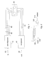
- a one-bit digital data recording system comprises a demultiplexer 10 for receiving an input one-bit digital audio signal 20, a data recorder 30 (in this case, a so-called AES/EBU standard digital audio recorder), and a multiplexer 40 for generating an output one-bit digital audio signal 50.
- Bit-inverters 60 and 70 are connected between the demultiplexer 10 and the data recorder 30 and between the data recorder 30 and the multiplexer 40.
- the input one-bit signal 20 comprises successive individual data bits: b 1 , b 2 , b 3 , b 4 , b 5 , b 6 , b 7 , ..., ... b 63 , b 64 , b 65 , b 66 , ...
- the AES/EBU recorder 30 is designed to record 16-bit data words (each representing a PCM audio sample) at a sampling rate of 48kHz.
- the demultiplexer 10 forms groups of the data bits of the one-bit input signal and passing them to the AES/EBU recorder 30 for recording as though they were 16-bit PCM data words.
- the one-bit digital audio signal has a data rate (bit rate) of 64fs, where fs is 48kHz, and so for each sample period of the 48kHz AES/EBU recorder, 64 bits of the one-bit digital audio signal must be multiplexed and recorded as data words. Therefore, four 16-bit data words are required to be formed for each 48kHz sample period.
- Four data words per sample period correspond to four audio channels being recorded on the AES/EBU data recorder. In fact, this can be configured as two stereo channels to accommodate the four data words per sample period.
- the two stereo channels are represented by pairs of signals 80, 90 in Figure 1 1 .
- bit streams each comprising alternate data bits from the input one-bit signal. Therefore, the bit streams would contain:
- Each of the two bit streams is then sub-divided to form the two channels of a respective stereo pair, for recording on the AES/EBU recorder. This is done by taking alternate groups of 16 adjacent bits and assigning them to one of the left and right channels of that stereo pair. So, using the notation established above, the following 16-bit data words would be generated for recording on the AES/EBU recorder 30:
- the inverters 60 invert the data bits of one of the stereo pairs before recording. Similar inverters 70 invert the same stereo pair when it is reproduced from the recorder 30. Because each stereo pair is formed from a respective bit stream, which in turn is formed of alternate bits of the input one-bit signal, the inverters 60 have the effect of inverting alternate bits of the input one-bit signal. These bits are then re-inverted on replay by the inverters 70 to reconstruct the bits of the input one-bit signal.
- the multiplexer 40 operates in a complementary manner to the demultiplexer 10, to convert replayed 16-bit data words into the one-bit signal b 1 , b 2 , b 3 , b 4 ...
- One advantage of this embodiment is that if there is an error which leads to a failure during replay on the AES/EBU recorder 30, that recorder will "mute" to a signal comprising successive digital zeroes. This is no problem in a PCM system, because a signal of all zeroes represents silence. However, in a one-bit signal, a signal of all zeroes represents a very loud noise indeed.
- the inverters 70 are operable to invert alternate bits output by the AES/EBU recorder (alternate in the sense that they become alternate within the one-bit signal output by the multiplexer 40), a mute signal is transformed into an output one-bit signal comprising alternate ones and zeroes.
- a signal of alternate ones and zeroes is a close representation of silence in a one-bit system.
- a mute signal may also be output and will be treated in the same way.
- the recorder 30 may be replaced by a transmission medium such as a cable, optical fibre or satellite link. If the transmission medium is disconnected or fails in any other way, or if it mutes through any transmission problems, then the inverters 70 have the same effect of transforming a PCM digital silence into a one-bit digital silence signal.
- a transmission medium such as a cable, optical fibre or satellite link.
- any inversion pattern which results in a silence signal having a substantially even distribution of ones and zeroes could perform the same function, and indeed there can be advantages in using an inversion pattern which inverts, perhaps, four bits at "random" positions within each 8-bit group of the input one-bit signal, to "spread out” the spectral energy of the "digital silence" signal.
- an inversion pattern which inverts, perhaps, four bits at "random" positions within each 8-bit group of the input one-bit signal, to "spread out” the spectral energy of the "digital silence” signal.
- Figure 2 schematically illustrates a generic bit inverter which could perform this function in place of the inverters 60 and 70.
- bit stream to be inverted is supplied on an input 100, and a bit-inverted bit stream is generated at an output 110.
- the inversion is performed by an exclusive-OR gate 120, which acts on two inputs: the input signal 100 and a bit stream generated by a shift register 130 connected in a feedback arrangement so that it repeatedly supplies a sequence of (in this case) eight bits to the exclusive-OR gate 120.
Abstract
Description
b1, b2, b3, b4, b5, b6, b7, ..., ... b63, b64, b65, b66, ...
- bit stream 1:
- b1, b3, b5, b7, ...
- bit stream 2:
- b4, b6, b8, ...
- left:
- b1, b3, b5 ... b29, b31
- right:
- b33, b35, b37, b39 ... b61, b63
- left:
- b2, b4, b6 ... b30, b32
- right:
- b34, b36, b38, b40 ... b62, b64
Claims (15)
- Apparatus for storing and/or transmitting a one-bit digital signal, the apparatus comprising:an input inverter for inverting a subset of the data bits of an input one-bit digital signal, to generate a bit-inverted signal;a storage and/or transmission medium for storing and/or transmitting the bit-inverted signal; andan output inverter for inverting the subset of the data bits of the bit-inverted signal, to regenerate the input one-bit digital signal.
- Apparatus according to claim 1, in which the storage and/or transmission medium is operable to store and/or transmit data words each having a predetermined number of data bits.
- Apparatus according to claim 2, in which:the storage and/or transmission medium is an AES/EBU standard digital audio recorder; andthe predetermined number of bits in each data word is 16 bits.
- Apparatus according to claim 2 or claim 3, comprising:a multiplexer for multiplexing data bits of the input one-bit signal into data words each having the predetermined number of data bits;the input inverter being operable to invert a subset of data words output by the multiplexer, to form the bit-inverted signal.
- Apparatus according to claim 4, in which the multiplexer is operable:to multiplex the input one-bit digital signal into two bit streams respectively formed of alternate data bits of the input one-bit digital signal; andto form data words from the bit streams, the data words for each bit stream comprising groups of successive bits of that bit stream.
- Apparatus according to claim 4 or claim 5, in which the output inverter is operable to invert the subset of data words of the bit-inverted signal;the apparatus comprising a demultiplexer for demultiplexing data words output by the output inverter, to regenerate the input one-bit digital signal.
- Apparatus according to any one of the preceding claims, in which the subset of data bits of the input one-bit digital signal inverted by the input inverter comprises substantially one half of the data bits of the input one-bit digital signal.
- Apparatus according to any one of the preceding claims, in which the input inverter is operable to invert alternate data bits of the input one-bit digital signal.
- Apparatus according to any one of claims 1 to 3, in which the input inverter comprises:means for providing an inversion control signal having a signal state varying between two predetermined states; andcontrol logic operable to selectively invert data bits of the input one-bit digital signal in response to a current state of the inversion control signal.
- Apparatus according to claim 9, in which:the providing means comprises a shift register having a one-bit output fed back to an input of the shift register; andthe control logic comprises an exclusive-OR gate operable to combine a current bit output by the shift register with a current bit of the input one-bit digital signal.
- Apparatus according to any one of the preceding claims, in which the storage and/or transmission medium is operable to output a mute signal comprising successive data bits of the same data value if a storage, reproduction and/or transmission error, failure or cessation occurs.
- Apparatus for formatting a one-bit digital signal for storage and/or transmission, the apparatus comprising an inverter for inverting a subset of the data bits of an input one-bit digital signal, to generate a bit-inverted signal to be stored or transmitted.
- Apparatus for receiving a one-bit digital signal after storage and/or transmission, the apparatus comprising an inverter for inverting a subset of the data bits of the received one-bit digital signal.
- Apparatus according to any one of the preceding claims, in which the input one-bit digital signal is a one-bit digital audio signal.
- A method of storing and/or transmitting a one-bit digital signal, the method comprising the successive steps of:(i) inverting a subset of the data bits of an input one-bit digital signal, to generate a bit-inverted signal;(ii) storing and/or transmitting the bit-inverted signal; and(iii) inverting the subset of the data bits of the bit-inverted signal, to regenerate the input one-bit digital signal.
Applications Claiming Priority (2)
| Application Number | Priority Date | Filing Date | Title |
|---|---|---|---|
| GB9624670A GB2319930B (en) | 1996-11-27 | 1996-11-27 | Storage and transmission of one-bit data |
| GB9624670 | 1996-11-27 |
Publications (3)
| Publication Number | Publication Date |
|---|---|
| EP0845779A2 true EP0845779A2 (en) | 1998-06-03 |
| EP0845779A3 EP0845779A3 (en) | 1999-05-26 |
| EP0845779B1 EP0845779B1 (en) | 2005-05-25 |
Family
ID=10803566
Family Applications (1)
| Application Number | Title | Priority Date | Filing Date |
|---|---|---|---|
| EP97307995A Expired - Lifetime EP0845779B1 (en) | 1996-11-27 | 1997-10-09 | Storage and transmission of one-bit data |
Country Status (6)
| Country | Link |
|---|---|
| US (1) | US6970753B2 (en) |
| EP (1) | EP0845779B1 (en) |
| JP (1) | JPH10215182A (en) |
| KR (1) | KR100488632B1 (en) |
| DE (1) | DE69733336T2 (en) |
| GB (1) | GB2319930B (en) |
Cited By (2)
| Publication number | Priority date | Publication date | Assignee | Title |
|---|---|---|---|---|
| EP1998331A1 (en) | 2007-05-30 | 2008-12-03 | Sony Corporation | Digital recording apparatus and method, digital reproduction apparatus and method, and digital data conversation apparatus |
| EP2107745A1 (en) * | 2008-03-31 | 2009-10-07 | Linear Technology Corporation | Method and system for bit polarization coding |
Families Citing this family (1)
| Publication number | Priority date | Publication date | Assignee | Title |
|---|---|---|---|---|
| FR2892244A1 (en) * | 2005-10-18 | 2007-04-20 | St Microelectronics Sa | Pulse density modulation sequence coherence detection circuit, e.g. for digital amplifier, has multiplexer suppressing analog signal based on control signal and generating square signal at frequency half of sequence oversampling frequency |
Citations (6)
| Publication number | Priority date | Publication date | Assignee | Title |
|---|---|---|---|---|
| JPS6394718A (en) * | 1986-10-09 | 1988-04-25 | Oki Electric Ind Co Ltd | Delta sigma type ad converter offset cancellation system |
| EP0385288A2 (en) * | 1989-03-02 | 1990-09-05 | ANT Nachrichtentechnik GmbH | Method for the time-division multiplex transmission of digital messages |
| JPH04331517A (en) * | 1991-05-02 | 1992-11-19 | Ricoh Co Ltd | Device and method for adding signal |
| EP0607714A1 (en) * | 1993-01-20 | 1994-07-27 | Schlumberger Industries S.A. | Multiple stage frequency modulated circuit |
| GB2287624A (en) * | 1994-03-03 | 1995-09-20 | Sony Corp | Audio signal processing circuits |
| EP0735461A1 (en) * | 1995-03-31 | 1996-10-02 | Sony Corporation | 1-Bit signal processing apparatus capable of amplitude modulation and recording or reproducing apparatus having loaded thereon the signal processing apparatus |
Family Cites Families (19)
| Publication number | Priority date | Publication date | Assignee | Title |
|---|---|---|---|---|
| DE2046964B2 (en) * | 1970-09-23 | 1973-02-15 | Siemens AG, 1000 Berlin u 8000 München | METHOD OF MEASURING BIT ERROR FREQUENCY IN SYNCHRONOUS TRANSMISSION |
| US3916179A (en) * | 1972-09-13 | 1975-10-28 | Westinghouse Electric Corp | Electronic integrator with voltage controlled time constant |
| US4142066A (en) * | 1977-12-27 | 1979-02-27 | Bell Telephone Laboratories, Incorporated | Suppression of idle channel noise in delta modulation systems |
| GB2101849A (en) * | 1981-06-01 | 1983-01-19 | Philips Electronic Associated | Encrypting digital signals for phase modulation on a carrier wave |
| GB2125654B (en) * | 1982-08-13 | 1986-01-29 | Hazeltine Corp | Intranetwork code division multiple access communication system |
| JPS6045978A (en) * | 1983-08-22 | 1985-03-12 | Nissan Motor Co Ltd | Method and apparatus for recording data |
| JPS6069928A (en) * | 1983-09-26 | 1985-04-20 | Pioneer Electronic Corp | Method for transmitting delta modulation signal |
| US4813040A (en) * | 1986-10-31 | 1989-03-14 | Futato Steven P | Method and apparatus for transmitting digital data and real-time digitalized voice information over a communications channel |
| GB8806452D0 (en) * | 1988-03-18 | 1988-04-20 | Imperial College | Digital data security system |
| NL8800988A (en) * | 1988-04-15 | 1989-11-01 | Philips Nv | SYSTEM FOR TRANSMISSION OF VIDEO SIGNALS WITH ADAPTIVE CODEWORD ALLOCATION, AND TRANSMITTER AND RECEIVER SUITABLE FOR THE SYSTEM. |
| US5142551A (en) * | 1991-02-28 | 1992-08-25 | Motorola, Inc. | Signal weighting system for digital receiver |
| US5550825A (en) * | 1991-11-19 | 1996-08-27 | Scientific-Atlanta, Inc. | Headend processing for a digital transmission system |
| US5347587A (en) * | 1991-11-20 | 1994-09-13 | Sharp Kabushiki Kaisha | Speaker driving device |
| US5283807A (en) * | 1992-10-21 | 1994-02-01 | Tutankhamon Electronics, Inc. | EMI suppression coding |
| US5451942A (en) * | 1994-02-04 | 1995-09-19 | Digital Theater Systems, L.P. | Method and apparatus for multiplexed encoding of digital audio information onto a digital audio storage medium |
| JP3465401B2 (en) * | 1994-03-03 | 2003-11-10 | ソニー株式会社 | Audio signal processing device and audio recording device |
| JP3238587B2 (en) * | 1994-12-27 | 2001-12-17 | バー−ブラウン・コーポレーション | Oversampling digital-to-analog converter with automatic muting function |
| SE507373C2 (en) * | 1996-09-06 | 1998-05-18 | Ericsson Telefon Ab L M | Device and method for pulse shaping and power amplification |
| US5793318A (en) * | 1997-02-05 | 1998-08-11 | Hewlett-Packard Company | System for preventing of crosstalk between a raw digital output signal and an analog input signal in an analog-to-digital converter |
-
1996
- 1996-11-27 GB GB9624670A patent/GB2319930B/en not_active Expired - Fee Related
-
1997
- 1997-07-03 JP JP9178557A patent/JPH10215182A/en not_active Withdrawn
- 1997-10-09 DE DE69733336T patent/DE69733336T2/en not_active Expired - Lifetime
- 1997-10-09 EP EP97307995A patent/EP0845779B1/en not_active Expired - Lifetime
- 1997-11-27 KR KR1019970063296A patent/KR100488632B1/en not_active IP Right Cessation
-
2001
- 2001-06-19 US US09/884,208 patent/US6970753B2/en not_active Expired - Fee Related
Patent Citations (6)
| Publication number | Priority date | Publication date | Assignee | Title |
|---|---|---|---|---|
| JPS6394718A (en) * | 1986-10-09 | 1988-04-25 | Oki Electric Ind Co Ltd | Delta sigma type ad converter offset cancellation system |
| EP0385288A2 (en) * | 1989-03-02 | 1990-09-05 | ANT Nachrichtentechnik GmbH | Method for the time-division multiplex transmission of digital messages |
| JPH04331517A (en) * | 1991-05-02 | 1992-11-19 | Ricoh Co Ltd | Device and method for adding signal |
| EP0607714A1 (en) * | 1993-01-20 | 1994-07-27 | Schlumberger Industries S.A. | Multiple stage frequency modulated circuit |
| GB2287624A (en) * | 1994-03-03 | 1995-09-20 | Sony Corp | Audio signal processing circuits |
| EP0735461A1 (en) * | 1995-03-31 | 1996-10-02 | Sony Corporation | 1-Bit signal processing apparatus capable of amplitude modulation and recording or reproducing apparatus having loaded thereon the signal processing apparatus |
Non-Patent Citations (1)
| Title |
|---|
| PATENT ABSTRACTS OF JAPAN vol. 017, no. 174 (E-1346), 5 April 1993 & JP 04 331517 A (RICOH CO LTD), 19 November 1992 * |
Cited By (4)
| Publication number | Priority date | Publication date | Assignee | Title |
|---|---|---|---|---|
| EP1998331A1 (en) | 2007-05-30 | 2008-12-03 | Sony Corporation | Digital recording apparatus and method, digital reproduction apparatus and method, and digital data conversation apparatus |
| US8154430B2 (en) | 2007-05-30 | 2012-04-10 | Sony Corporation | Digital recording apparatus and method, digital reproduction apparatus and method, and digital data conversion apparatus |
| EP2107745A1 (en) * | 2008-03-31 | 2009-10-07 | Linear Technology Corporation | Method and system for bit polarization coding |
| US7656337B2 (en) | 2008-03-31 | 2010-02-02 | Linear Technology Corporation | Method and system for bit polarization coding |
Also Published As
| Publication number | Publication date |
|---|---|
| GB9624670D0 (en) | 1997-01-15 |
| JPH10215182A (en) | 1998-08-11 |
| EP0845779A3 (en) | 1999-05-26 |
| GB2319930B (en) | 2001-05-16 |
| DE69733336T2 (en) | 2006-02-02 |
| KR19980042812A (en) | 1998-08-17 |
| US20020026254A1 (en) | 2002-02-28 |
| US6970753B2 (en) | 2005-11-29 |
| KR100488632B1 (en) | 2005-09-14 |
| GB2319930A (en) | 1998-06-03 |
| EP0845779B1 (en) | 2005-05-25 |
| DE69733336D1 (en) | 2005-06-30 |
Similar Documents
| Publication | Publication Date | Title |
|---|---|---|
| JP3038219B2 (en) | Device for transmitting and receiving data words representing digitized analog signals | |
| EP0599824B1 (en) | Intensity-stereo encoding and decoding in a transmission system | |
| NO951549D0 (en) | Multichannel transmission and / or storage of digital signals | |
| EP0820664B1 (en) | N-channel transmission, compatible with 2-channel transmission and 1-channel transmission | |
| US3629823A (en) | Information-handling system having error correction capabilities | |
| JP3993229B2 (en) | Transmission and reception of first and second main signal components | |
| EP0845779B1 (en) | Storage and transmission of one-bit data | |
| EA003213B1 (en) | Embedding a first digital information signal into a second digital information signal for transmission via a transmission medium | |
| CZ293070B6 (en) | Method and apparatus for encoding a plurality of digital information signals, a record medium and apparatus for decoding a received transmission signal | |
| US7088779B2 (en) | Method and apparatus for reducing the word length of a digital input signal and method and apparatus for recovering a digital input signal | |
| US4314369A (en) | Digital coding process for recording sound channels with a television signal and apparatus realizing this process | |
| JPH11298999A (en) | Multi-channel pcm sound signal transmitting system | |
| EP1151433B1 (en) | Data encoding/decoding device and apparatus using the same | |
| JPS59161948A (en) | Time division multiplexer | |
| RU2267171C2 (en) | Transmission of digital information signal, having m-byte selections of pulse-code modulation | |
| EP0996251A1 (en) | Sub-scrambling/descrambling method and sub-scrambling/descrambling device | |
| JP3185420B2 (en) | Multi-channel multiplexer | |
| KR100472402B1 (en) | Apparatus and method for encoding a plurality of information signals | |
| KR0157666B1 (en) | Audio scramble system, audio scramble apparatus and audio descramble apparatus | |
| JPH0378015B2 (en) | ||
| JPS5940731A (en) | Noise eliminating device | |
| JPH09330560A (en) | Preventing method for copying of code information, encoding device therefor, decoding device therefor, and recording medium | |
| JPH10106168A (en) | Digital disk player | |
| JP3365239B2 (en) | Code information copy protection method and decoding device | |
| KR930005438B1 (en) | Parallel processing discrambling circuit of decoding system for cdp |
Legal Events
| Date | Code | Title | Description |
|---|---|---|---|
| PUAI | Public reference made under article 153(3) epc to a published international application that has entered the european phase |
Free format text: ORIGINAL CODE: 0009012 |
|
| AK | Designated contracting states |
Kind code of ref document: A2 Designated state(s): DE FR NL |
|
| AX | Request for extension of the european patent |
Free format text: AL;LT;LV;RO;SI |
|
| PUAL | Search report despatched |
Free format text: ORIGINAL CODE: 0009013 |
|
| AK | Designated contracting states |
Kind code of ref document: A3 Designated state(s): AT BE CH DE DK ES FI FR GB GR IE IT LI LU MC NL PT SE |
|
| AX | Request for extension of the european patent |
Free format text: AL;LT;LV;RO;SI |
|
| 17P | Request for examination filed |
Effective date: 19991102 |
|
| AKX | Designation fees paid |
Free format text: DE FR NL |
|
| 17Q | First examination report despatched |
Effective date: 20021112 |
|
| GRAP | Despatch of communication of intention to grant a patent |
Free format text: ORIGINAL CODE: EPIDOSNIGR1 |
|
| GRAP | Despatch of communication of intention to grant a patent |
Free format text: ORIGINAL CODE: EPIDOSNIGR1 |
|
| GRAS | Grant fee paid |
Free format text: ORIGINAL CODE: EPIDOSNIGR3 |
|
| GRAA | (expected) grant |
Free format text: ORIGINAL CODE: 0009210 |
|
| AK | Designated contracting states |
Kind code of ref document: B1 Designated state(s): DE FR NL |
|
| REF | Corresponds to: |
Ref document number: 69733336 Country of ref document: DE Date of ref document: 20050630 Kind code of ref document: P |
|
| ET | Fr: translation filed | ||
| PLBE | No opposition filed within time limit |
Free format text: ORIGINAL CODE: 0009261 |
|
| STAA | Information on the status of an ep patent application or granted ep patent |
Free format text: STATUS: NO OPPOSITION FILED WITHIN TIME LIMIT |
|
| 26N | No opposition filed |
Effective date: 20060228 |
|
| PGFP | Annual fee paid to national office [announced via postgrant information from national office to epo] |
Ref country code: DE Payment date: 20141022 Year of fee payment: 18 Ref country code: FR Payment date: 20141022 Year of fee payment: 18 |
|
| PGFP | Annual fee paid to national office [announced via postgrant information from national office to epo] |
Ref country code: NL Payment date: 20141021 Year of fee payment: 18 |
|
| REG | Reference to a national code |
Ref country code: DE Ref legal event code: R119 Ref document number: 69733336 Country of ref document: DE |
|
| REG | Reference to a national code |
Ref country code: NL Ref legal event code: MM Effective date: 20151101 |
|
| PG25 | Lapsed in a contracting state [announced via postgrant information from national office to epo] |
Ref country code: DE Free format text: LAPSE BECAUSE OF NON-PAYMENT OF DUE FEES Effective date: 20160503 |
|
| REG | Reference to a national code |
Ref country code: FR Ref legal event code: ST Effective date: 20160630 |
|
| PG25 | Lapsed in a contracting state [announced via postgrant information from national office to epo] |
Ref country code: FR Free format text: LAPSE BECAUSE OF NON-PAYMENT OF DUE FEES Effective date: 20151102 Ref country code: NL Free format text: LAPSE BECAUSE OF NON-PAYMENT OF DUE FEES Effective date: 20151101 |