EP0844654A2 - Heat treatment method for a silicon wafer and a silicon wafer heat-treated by the method - Google Patents
Heat treatment method for a silicon wafer and a silicon wafer heat-treated by the method Download PDFInfo
- Publication number
- EP0844654A2 EP0844654A2 EP97309246A EP97309246A EP0844654A2 EP 0844654 A2 EP0844654 A2 EP 0844654A2 EP 97309246 A EP97309246 A EP 97309246A EP 97309246 A EP97309246 A EP 97309246A EP 0844654 A2 EP0844654 A2 EP 0844654A2
- Authority
- EP
- European Patent Office
- Prior art keywords
- heat treatment
- silicon wafer
- temperature
- wafer
- heat
- Prior art date
- Legal status (The legal status is an assumption and is not a legal conclusion. Google has not performed a legal analysis and makes no representation as to the accuracy of the status listed.)
- Ceased
Links
Images

Classifications
-
- H—ELECTRICITY
- H01—ELECTRIC ELEMENTS
- H01L—SEMICONDUCTOR DEVICES NOT COVERED BY CLASS H10
- H01L21/00—Processes or apparatus adapted for the manufacture or treatment of semiconductor or solid state devices or of parts thereof
- H01L21/02—Manufacture or treatment of semiconductor devices or of parts thereof
- H01L21/04—Manufacture or treatment of semiconductor devices or of parts thereof the devices having at least one potential-jump barrier or surface barrier, e.g. PN junction, depletion layer or carrier concentration layer
- H01L21/18—Manufacture or treatment of semiconductor devices or of parts thereof the devices having at least one potential-jump barrier or surface barrier, e.g. PN junction, depletion layer or carrier concentration layer the devices having semiconductor bodies comprising elements of Group IV of the Periodic System or AIIIBV compounds with or without impurities, e.g. doping materials
- H01L21/30—Treatment of semiconductor bodies using processes or apparatus not provided for in groups H01L21/20 - H01L21/26
- H01L21/322—Treatment of semiconductor bodies using processes or apparatus not provided for in groups H01L21/20 - H01L21/26 to modify their internal properties, e.g. to produce internal imperfections
- H01L21/3221—Treatment of semiconductor bodies using processes or apparatus not provided for in groups H01L21/20 - H01L21/26 to modify their internal properties, e.g. to produce internal imperfections of silicon bodies, e.g. for gettering
- H01L21/3225—Thermally inducing defects using oxygen present in the silicon body for intrinsic gettering
Definitions
- the present invention relates to a heat treatment method for reducing in a simple and reliable manner micro-defects which exist in the surface of a single-crystal wafer of semiconductor silicon.
- the present invention also relates to a silicon wafer which is heat-treated by the above method.
- Such silicon wafers are manufactured in a manner in which a cylindrical single-crystal silicon ingot is sliced into wafers, and the surfaces of the sliced wafers are then mirror-polished.
- a single-crystal silicon ingot is usually manufactured by the Czochralski method (pulling method).
- CZ silicon wafers manufactured from a single-crystal silicon ingot grown by the Czochralski method contain micro-defects which are generated due to precipitation of oxygen or the like and which serve as nuclei of oxidation induced stacking faults and crystal defects (grown-in defects) called COP (crystal originated particles).
- COP crystal originated particles
- This method is effective to a certain degree for the reduction of oxidation induced stacking faults in the surface of a wafer.
- the method is dangerous due to the use of hydrogen gas as a heat treatment ambient gas.
- a heat treatment apparatus must employ a special explosion-proof feature, which makes the apparatus complex and expensive and involves complicated operations.
- the heat treatment time is relatively long. From the viewpoint of the process time extending from loading of wafers into a heat treatment furnace to unloading therefrom, the method is poor in productivity and high in cost. Additionally, the surfaces of the thus-heat-treated wafer still contain approximately 50 oxidation induced stacking faults per square centimeter.
- a heat treatment method which does not use hydrogen is proposed in Japanese Patent Application Laid-Open ( kokai ) No. 7-45622. According to this method, until wafers reach a temperature of 1100°C to 1200°C, in a non-oxidation atmosphere the wafers are heated at such a temperature-rising rate as not to cause slip dislocation in the wafers, and then cooled at such a temperature-lowering rate as not to cause slip dislocation in the wafers.
- This method is also effective to a certain degree for the reduction of oxidation induced stacking faults, but requires a relatively long time for heat treatment.
- a temperature-rising or -lowering rate as not to cause slip dislocation in a wafer means, for example, 20°C/min to 30°C/min, indicating that time required for loading wafers into or unloading from a heat treatment furnace is relatively long.
- the overall process time covering loading, heat treatment, and unloading is relatively long, so that this method is also poor in productivity and high in cost.
- wafers at room temperature are gradually loaded at a speed of 15 cm/min into a heat treatment furnace maintained at a temperature lower than 1000°C.
- the heat treatment furnace is heated to a desired temperature at a slow rate of, for example, 10°C/min.
- the heat treatment furnace is cooled to a temperature lower than 1000°C at a slow rate of, for example, 5°C/min.
- the heat-treated wafers are unloaded from the heat treatment furnace at a slow speed; for example, a speed identical to the loading speed.
- each step of the heat treatment process specifically loading of wafers into a heat treatment furnace, temperature raising, heat treatment, temperature lowering, and unloading, requires a relatively long time.
- the overall productivity of the heat treatment process is reduced, and the heat treatment cost increases significantly.
- the present invention has been accomplished to solve the above-mentioned problems, and an object of the present invention is to provide a low-cost heat treatment method for a silicon wafer capable of removing crystal defects and micro-defects which are present in the vicinity of the surface of a silicon wafer and serve as nuclei of oxidation stacking faults, in a simple and reliable manner and within a short period of time, with no use of gas endangering safety such as hydrogen, and no use of a special apparatus associated with use of such a dangerous gas.
- Another object of the present invention is to provide a silicon wafer manufactured in accordance with the above heat treatment method.
- the present invention provides a heat treatment method for a silicon wafer comprising the steps of: loading a silicon wafer, on which a natural oxide film is formed at least at the surface thereof, directly into a heat treatment furnace heated to a temperature within the range of 1000°C to the melting point of silicon; heat-treating the silicon wafer at a temperature within the range; and unloading the silicon wafer having a temperature within the range from the heat treatment furnace immediately after the heat treatment is completed.
- micro-defects which serve as nuclei of oxidation induced stacking faults can be reduced.
- a silicon wafer is loaded directly into a high-temperature heat treatment furnace and unloaded from the furnace immediately after the heat treatment is completed.
- loading and unloading operations are completed in a negligibly short period of time, and temperature-raising and -lowering operations are not involved, thereby carrying out the heat treatment process in a very short period of time.
- hydrogen is not used as an ambient gas for heat treatment, so that an ordinary heat treatment furnace can be employed for heat treatment of silicon wafers.
- a natural oxide film must be formed on the surfaces of a silicon wafer to be heat-treated. This prevents the surfaces of a silicon wafer from altering due to thermal nitriding or etching which would otherwise be induced by heat treatment, and from being contaminated with impurities.
- the natural oxide film is intentionally formed by cleaning a silicon wafer to be heat-treated in an acid or alkali cleaning solution containing hydrogen peroxide.
- a natural oxide film formed merely by allowing a silicon wafer to stand in the atmosphere or by rinsing a silicon wafer in pure water is thin and coarse, so that the aforementioned alteration or contamination may not be prevented. In actuality, the thus-formed natural oxide film itself may be contaminated while being left in the atmosphere.
- a silicon wafer is heat-treated at a temperature ranging from 1200°C to 1350°C.
- Heat treatment in such a high temperature range efficiently annihilates micro-defects which serve as nuclei of oxidation induced stacking faults, and reduces heat treatment time. Thus, wafers are less contaminated.
- an ambient gas for heat treatment is nitrogen, inert gas, a mixture of nitrogen and inert gas, or a mixture of any of these gases and oxygen and/or water vapor.
- Such an ambient gas prevents the surface of a wafer from altering or being contaminated during heat treatment.
- the time of heat treatment is 1 second to 2 minutes.
- micro-defects which serve as nuclei of oxidation induced stacking faults of various sizes can be sufficiently annihilated, thereby improving productivity.
- the present invention provides a silicon wafer which is heat-treated by the method of the invention, thereby having few micro-defects which serve as nuclei of oxidation induced stacking defects. Therefore, silicon wafers of considerably high quality can be obtained.
- the present invention through heat treatment over a very short period of time, micro-defects which serve as nuclei of oxidation induced stacking faults in the surfaces of silicon wafers can be sufficiently annihilated.
- the heat treatment does not use any dangerous gas such as hydrogen, a special apparatus is not required. Therefore, the present invention enables silicon wafers of high quality to be manufactured at lower cost, and can be valuably utilized in the industries.
- nuclei of oxidation induced stacking faults tend to grow due to wafers being gradually heated from room temperature to a certain high temperature; consequently, wafers must undergo high-temperature heat treatment for 30 minutes or longer in the aforementioned hydrogen ambient or non-oxidation ambient in order to annihilate the grown nuclei.
- nuclei of oxidation induced stacking faults begin to melt.
- nitrogen when nitrogen is used as an ambient gas, nitrogen supplies vacancies into a wafer through the surface thereof, nuclei of oxidation induced stacking faults at the surface of the wafer can be annihilated very effectively. Nevertheless, heat treatment must be carried out for a long time of 30 minutes or longer in a hydrogen ambient or non-oxidation ambient as mentioned above. This is because a wafer is gradually heated to a high temperature at which nuclei of oxidation induced stacking faults are annihilated, and consequently nuclei have grown during this gradual temperature rise.
- the present inventors therefore, have taken an approach of heating a wafer to a desired high temperature as quick as possible instead of gradually so as not to allow growth of nuclei of oxidation induced stacking defects, whereby the nuclei are annihilated by high-temperature heat treatment over a short period of time.
- the present invention was accomplished based on the above-described idea.
- a silicon wafer is directly loaded into a heat treatment furnace maintained at a desired high temperature and unloaded from the furnace immediately after the heat treatment is completed, in contrast with a conventional method in which a wafer is gradually loaded into a heat treatment furnace, the furnace is then gradually heated to a desired high temperature, the furnace is gradually cooled after the heat treatment is completed, and then the wafer is gradually unloaded from the furnace.
- nuclei of oxidation induced stacking faults remain ungrown. Thus, the nuclei can be annihilated by high-temperature heat treatment over a short period of time.
- the heat treatment time can be significantly reduced, so that productivity is far improved as compared with conventional methods. Further, since the method of the present invention requires no special apparatus, such as that required when hydrogen gas is used, low-cost heat treatment is achieved.
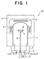
- FIG. 1 shows an example of a heat treatment furnace for heat-treating a wafer at a high temperature according to the method of the present invention.
- a heat-treatment furnace 10 of FIG. 1 includes a bell jar 1 which is formed from, for example, silicon carbide and in which a wafer is heat-treated. Heaters 2 and 2' surround the bell jar 1 so as to heat the bell jar 1. The heater 2' is separated from the heater 2 along a vertical direction. Also, power supplied to the heater 2' is independent of that to the heater 2 for independent power control between the heaters 2 and 2'. The heating method is not limited thereto, but so-called radiation heating and induction heating may also be applicable.
- the bell jar 1 and the heaters 2 and 2' are housed in a housing 3 serving as a heat shield.
- a water-cooled chamber 4 and a base plate 5 are arranged at the lower portion of a furnace so as to isolate the interior of the bell jar 1 from the atmosphere.
- a wafer 8 is held on a stage 7, which is attached to the top end of a support shaft 6, which, in turn, is moved vertically by means of a motor 9.
- the water-cooled chamber 4 has an unillustrated wafer port which is opened and closed by means of a gate valve.
- a gas inlet and a gas outlet are provided in the base plate 5 so that the gas ambient within the furnace can be adjusted.
- a heat treatment method of the present invention is carried out in the procedure described below.
- the interior of the bell jar 1 is heated to a desired temperature ranging from 1000°C to the melting point of silicon by the heaters 2 and 2' and is then held at the desired temperature.
- a temperature distribution can be established within the bell jar 1 along a vertical direction. Accordingly, the heat-treatment temperature of a wafer is determined by the position of the stage 7, i.e. the amount of insertion of the support shaft 6 into the furnace.
- a wafer is inserted through the wafer port of the water-cooled chamber 4 by an unillustrated wafer handling apparatus arranged by the heat treatment furnace 10.
- the inserted wafer is placed in, for example, an SiC boat provided on the stage 7 which is situated at the bottom standby position. Since the water-cooled chamber 4 and the base plate 5 are water-cooled, the wafer located at this standby position is not heated to a high temperature.
- the motor 9 Upon completion of placing the wafer on the stage 7, the motor 9 is immediately driven to insert the support shaft 6 into the furnace so that the stage 7 is raised to a heat treatment position where a desired temperature ranging from 1000°C to the melting point of silicon is established (hereinafter referred to as the "desired temperature position"), thereby heat-treating the wafer at the temperature.
- a desired temperature ranging from 1000°C to the melting point of silicon
- the desired temperature position a desired temperature ranging from 1000°C to the melting point of silicon
- the stage 7 is halted at the desired temperature position for a predetermined time, thereby subjecting the wafer to high-temperature heat treatment over the halting time.
- the motor 9 is immediately driven to withdraw the support shaft 6 from the interior of the furnace down to the bottom standby position in the water-cooled chamber 4. This lowering motion can be completed in approximately 20 seconds, for example.
- the wafer on the stage 7 is quickly cooled, since the water-cooled chamber 4 and the base plate 5 are water-cooled. Finally, the wafer is unloaded from inside the water-cooled chamber 4 by the wafer handling apparatus, thus completing the heat treatment.
- these wafers can be sequentially loaded into and heat-treated in the heat treatment furnace 10 maintained at a predetermined high temperature.
- a silicon wafer is directly loaded into a heat treatment furnace heated to a temperature ranging from 1000°C to the melting point of silicon, the silicon wafer undergoes heat treatment at a temperature of the range, and then the silicon wafer heated to a temperature of the range is unloaded from the heat treatment furnace immediately after the heat treatment is completed.
- the present invention does not involve the operations of gradually loading a wafer into and unloading from a heat treatment furnace and raising and lowering the temperature of the heat treatment furnace.
- moving a wafer to a desired heat treatment position in a furnace requires a certain time, which depends on the capability of a moving apparatus and may range from several seconds to several minutes.
- nuclei of oxidation induced stacking faults do not grow.
- nuclei of oxidation induced stacking faults can be reliably annihilated. Further, since the overall time of the heat treatment process can be reduced, an improvement in productivity and cost is attained.
- a natural oxide film must be formed on the surfaces of a silicon wafer to be heat-treated. This means that heat treatment of the present invention must not be carried out immediately after a silicon wafer undergoes etching or cleaning with hydrofluoric acid, which removes an oxide film from the surfaces of a silicon wafer.
- heat treatment of the present invention will alters the surfaces of a silicon wafer due to thermal nitriding or etching or cause contamination with impurities.
- this natural oxide film is intentionally formed by cleaning a silicon wafer to be heat-treated in an acid or alkali cleaning solution containing hydrogen peroxide.
- Silicon wafers are always cleaned before heat treatment. Therefore, if a natural oxide film is formed in the cleaning step, no additional step is required, and therefore the process can be made efficient.
- a natural oxide film formed merely by allowing a silicon wafer to stand in the atmosphere or rinsing a silicon wafer in pure water is thin and coarse, so that the alteration or contamination of the surfaces of a wafer may not be prevented in heat treatment. In actuality, the thus-formed natural oxide film itself may be contaminated while being left in the atmosphere.
- Examples of acid containing hydrogen peroxide include a mixture of hydrochloric acid and hydrogen peroxide, while examples of alkali include a mixture of hydrogen peroxide and NH 3 , KOH, and NaOH.
- the present invention is not limited thereto. Any other cleaning solutions capable of causing a fine natural oxide film to be formed on the surfaces of a wafer are acceptable.
- the temperature of heat treatment according to the present invention ranges from 1000°C to the melting point of silicon, particularly from 1200°C to 1350°C.
- the temperature range of 1000°C to the melting point of silicon is effective for annihilation of micro-defects which serve as nuclei of oxidation induced stacking faults.
- a temperature in excess of 1350°C is close to the melting point of silicon; consequently, the shape of a wafer may deform, and continuously operating a heat treatment furnace at such a high temperature may raise a problem in heat resistance of the heat treatment furnace.
- a temperature lower than 1200°C slows the rate of annihilation of nuclei of oxidation induced stacking faults, resulting in longer time of heat treatment. As the time of heat treatment increases, a wafer is more likely to be contaminated.
- a heat treatment temperature ranging from 1200°C to 1350°C enables efficient annihilation of micro-defects which serve as nuclei of oxidation induced stacking faults, and allows the time of heat treatment to be reduced, thereby reducing contamination of a wafer.
- the time of heat treatment is preferably 1 second to 2 minutes.
- nuclei of oxidation induced stacking faults do not grow, so that heat treatment for at most 2 minutes is sufficient. If a wafer is heat-treated for over 2 minutes, the wafer may be contaminated. Also, for reliable annihilation of oxidation induced stacking faults, a wafer is preferably heat-treated for at least 1 second or so.
- heat treatment according to the present invention can sufficiently annihilate micro-defects which serve as nuclei of oxidation induced stacking faults, within a very short period of time.
- a preferred ambient gas for heat treatment is nitrogen, inert gas, a mixture of nitrogen and inert gas, or a mixture of any of these gases and oxygen and/or water vapor.
- Such a gas ambient in combination with a natural oxide film formed on a wafer, suppresses alteration or contamination of the surfaces of a wafer during heat treatment.
- nitrogen as an ambient gas does not involve contamination of a wafer or danger as in the case where hydrogen is used.
- silicon and nitrogen react with each other on the surfaces of a wafer, the surfaces will be nitrided. Therefore, a natural oxide film must be formed on the surfaces of a wafer.
- high-temperature heat treatment in a 100% nitrogen ambient may cause a natural oxide film to evaporate with resultant partial nitriding of the surfaces of a wafer, adding a small amount of oxygen or water vapor to nitrogen is more effective.
- a single-crystal silicon ingot 6 inches (approx. 155 mm) dia., p type, 8-12 ⁇ cm, orientation: ⁇ 100> was pulled by the Czochralski method.
- a single-crystal silicon ingot is usually pulled at a speed of approximately 1 mm/min or more, but was intentionally pulled at a speed of approximately 0.75 mm/min so that nuclei of oxidation induced stacking defects were more likely to generate in a ring shape in the grown crystal bar.
- these silicon mirror wafers were cleaned in a mixture solution of hydrogen peroxide and NH 3 and then rinsed with pure water to thereby form a natural oxide film having a thickness of approximately 20 angstroms on the surfaces of the wafers.
- Heat treatment was carried out in a gas ambient consisting of 99% of nitrogen and 1% of oxygen at 1250°C for 1 second.
- the wafer underwent the normal preparatory treatment for measurement of oxidation induced stacking faults. Specifically, the wafer underwent heat treatment at 1200°C for 100 minutes in a pyrogenic oxidation ambient. Further, the surfaces of the wafer were lightly etched with a mixed acid of hydrofluoric acid, nitric acid, dichromic acid, and acetic acid. Thereafter, the density of oxidation induced stacking faults was measured through a microscope at intervals of 5 mm from the center of the wafer. Measurements of the density of oxidation induced stacking faults were up to 50 faults/cm 2 . (See FIGS. 2 and 3.)
- Another one of the aforementioned six silicon wafers was not subjected to heat treatment according to the present invention and measured for the density of oxidation induced stacking faults. As a result, the measured maximum density of oxidation induced stacking faults was in excess of 7000 faults/cm 2 . (See FIG. 2.)
- a further one of the aforementioned six silicon wafers was subjected to high-temperature heat treatment according to the present invention under conditions similar to those of Example 1 except that the time of heat treatment was 5 seconds. Subsequently, the wafer was measured for the density of oxidation induced stacking faults. As a result, measurements of the density of oxidation induced stacking faults were up to 20 faults/cm 2 . (See FIG. 3.)
- Still another one of the aforementioned six silicon wafers was subjected to high-temperature heat treatment according to the present invention under conditions similar to those of Example 1 except that the time of heat treatment was 10 seconds. Subsequently, the wafer was measured for the density of oxidation induced stacking faults. As a result, measurements of the density of oxidation induced stacking faults were up to 20 faults/cm 2 . (See FIG. 3.)
- a still further one of the aforementioned six silicon wafers was subjected to high-temperature heat treatment according to the present invention under conditions similar to those of Example 1 except that the time of heat treatment was 20 seconds. Subsequently, the wafer was measured for the density of oxidation induced stacking faults. As a result, measurements of the density of oxidation induced stacking faults were up to 20 faults/cm 2 . (See FIG. 3.)
- a still further one of the aforementioned six silicon wafers was subjected to high-temperature heat treatment according to the present invention under conditions similar to those of Example 1 except that the time of heat treatment was 40 seconds. Subsequently, the wafer was measured for the density of oxidation induced stacking faults. As a result, measurements of the density of oxidation induced stacking faults was up to 20 faults/cm 2 . (See FIG. 3.)
- the silicon wafers of Examples 1 to 5 were free from generation of hazes due to nitriding at wafer surfaces and generation of slip dislocations, both of which might have occurred due to heat treatment of the present invention. Further, the silicon wafers of Examples 1 to 5 were free from other kinds of crystal defects.
- the method of the present invention can reliably annihilate oxidation induced stacking faults through heat treatment over a short period of time.
- the present invention is not limited to the above-described embodiment.
- the above-described embodiment is a mere example, and those having the substantially same structure as that described in the appended claims and providing the similar action and effects are included in the scope of the present invention.
- a heat treatment furnace as shown in FIG. 1 is used.
- the present invention is not limited thereto. In principle, any furnaces may be used so long as they are ordinarily used for heat treatment of silicon wafers and can be heated to a temperature of 1000°C or higher.
Abstract
Description
Claims (6)
- A heat treatment method for a silicon wafer, characterized in that a silicon wafer, on which a natural oxide film is formed at least at the surface thereof, is loaded directly into a heat treatment furnace heated to a temperature within a temperature range of 1000°C to the melting point of silicon; the silicon wafer is heat-treated at a temperature within the temperature range; and the silicon wafer having a temperature within the temperature range is unloaded from the heat treatment furnace immediately after the heat treatment is completed.
- A heat treatment method for a silicon wafer according to Claim 1, characterized in that the natural oxide film is intentionally formed by cleaning the silicon wafer to be heat-treated in an acid or alkali cleaning solution containing hydrogen peroxide.
- A heat treatment method for a silicon wafer according to Claim 1 or 2, characterized in that the silicon wafer is heat-treated at a temperature in a range of 1200°C to 1350°C.
- A heat treatment method for a silicon wafer according to any one of Claims 1 - 3, characterized in that the heat treatment is performed in the presence of an ambient gas selected from the group consisting of nitrogen, inert gas, a mixture of nitrogen and inert gas, and a mixture of any of these gases and at least one of oxygen and water vapor.
- A heat treatment method for a silicon wafer according to any one of Claims 1 - 4, characterized in that the heat treatment is performed for a period of 1 second to 2 minutes.
- A silicon wafer which is heat-treated by the method according to any one of Claims 1 - 5, thereby having few micro-defects which serve as nuclei of oxidation induced stacking defects.
Applications Claiming Priority (2)
| Application Number | Priority Date | Filing Date | Title |
|---|---|---|---|
| JP8327734A JPH10154713A (en) | 1996-11-22 | 1996-11-22 | Silicon wafer and its heat-treating method |
| JP327734/96 | 1996-11-22 |
Publications (2)
| Publication Number | Publication Date |
|---|---|
| EP0844654A2 true EP0844654A2 (en) | 1998-05-27 |
| EP0844654A3 EP0844654A3 (en) | 1999-01-27 |
Family
ID=18202394
Family Applications (1)
| Application Number | Title | Priority Date | Filing Date |
|---|---|---|---|
| EP97309246A Ceased EP0844654A3 (en) | 1996-11-22 | 1997-11-18 | Heat treatment method for a silicon wafer and a silicon wafer heat-treated by the method |
Country Status (4)
| Country | Link |
|---|---|
| US (1) | US6204188B1 (en) |
| EP (1) | EP0844654A3 (en) |
| JP (1) | JPH10154713A (en) |
| TW (1) | TW355820B (en) |
Cited By (2)
| Publication number | Priority date | Publication date | Assignee | Title |
|---|---|---|---|---|
| CN105624795A (en) * | 2016-03-09 | 2016-06-01 | 中国科学院上海微系统与信息技术研究所 | Heat treatment method for n-type silicon wafer |
| DE102016125340A1 (en) * | 2016-12-22 | 2018-06-28 | Infineon Technologies Ag | A method of forming a semiconductor substrate, a method of forming a semiconductor device, a semiconductor substrate, and a semiconductor device |
Families Citing this family (10)
| Publication number | Priority date | Publication date | Assignee | Title |
|---|---|---|---|---|
| WO1999010570A1 (en) * | 1997-08-26 | 1999-03-04 | Sumitomo Metal Industries, Ltd. | High-quality silicon single crystal and method of producing the same |
| JP3487334B2 (en) * | 1998-07-17 | 2004-01-19 | 三菱住友シリコン株式会社 | Method for analyzing impurities in silicon substrate |
| WO2000012786A1 (en) * | 1998-08-31 | 2000-03-09 | Shin-Etsu Handotai Co., Ltd. | Method for producing silicon single crystal wafer and silicon single crystal wafer |
| DE69908965T2 (en) * | 1998-10-14 | 2004-05-13 | Memc Electronic Materials, Inc. | HEAT TEMPERATURE SINGLE CRYSTAL SILICON WITH LOW ERROR DENSITY |
| JP2000256092A (en) * | 1999-03-04 | 2000-09-19 | Shin Etsu Handotai Co Ltd | Silicon wafer |
| JP4633977B2 (en) * | 2001-08-30 | 2011-02-16 | 信越半導体株式会社 | Annealed wafer manufacturing method and annealed wafer |
| JP4524983B2 (en) * | 2002-10-22 | 2010-08-18 | 信越半導体株式会社 | Method for manufacturing silicon wafer |
| JP5223771B2 (en) * | 2009-05-08 | 2013-06-26 | 東京エレクトロン株式会社 | Film forming method, gate electrode structure forming method and processing apparatus |
| JP5565079B2 (en) * | 2010-05-10 | 2014-08-06 | 信越半導体株式会社 | Manufacturing method of SOI wafer |
| MY188961A (en) * | 2013-07-01 | 2022-01-14 | Solexel Inc | High-throughput thermal processing methods for producing high-efficiency crystalline silicon solar cells |
Citations (6)
| Publication number | Priority date | Publication date | Assignee | Title |
|---|---|---|---|---|
| US4432809A (en) * | 1981-12-31 | 1984-02-21 | International Business Machines Corporation | Method for reducing oxygen precipitation in silicon wafers |
| US4868133A (en) * | 1988-02-11 | 1989-09-19 | Dns Electronic Materials, Inc. | Semiconductor wafer fabrication with improved control of internal gettering sites using RTA |
| DE4142466A1 (en) * | 1991-12-20 | 1993-06-24 | Siemens Ag | Accelerating cooling in rapid thermal annealing of semiconductor wafer - using rows of light sources by moving reflector plates to reduce reflection |
| US5279973A (en) * | 1990-10-16 | 1994-01-18 | Kabushiki Kaisha Toshiba | Rapid thermal annealing for semiconductor substrate by using incoherent light |
| US5352615A (en) * | 1994-01-24 | 1994-10-04 | Motorola, Inc. | Denuding a semiconductor substrate |
| US5445975A (en) * | 1994-03-07 | 1995-08-29 | Advanced Micro Devices, Inc. | Semiconductor wafer with enhanced pre-process denudation and process-induced gettering |
Family Cites Families (14)
| Publication number | Priority date | Publication date | Assignee | Title |
|---|---|---|---|---|
| US4784975A (en) * | 1986-10-23 | 1988-11-15 | International Business Machines Corporation | Post-oxidation anneal of silicon dioxide |
| US5011794A (en) * | 1989-05-01 | 1991-04-30 | At&T Bell Laboratories | Procedure for rapid thermal annealing of implanted semiconductors |
| JPH0758698B2 (en) * | 1990-08-22 | 1995-06-21 | 信越半導体株式会社 | Boron diffusion method to semiconductor wafer |
| CA2059841A1 (en) * | 1991-01-24 | 1992-07-25 | Ichiro Hayashida | Surface treating solutions and cleaning method |
| KR940009597B1 (en) * | 1991-08-22 | 1994-10-15 | 삼성전자 주식회사 | Forming method of gate oxide film |
| US5308400A (en) * | 1992-09-02 | 1994-05-03 | United Microelectronics Corporation | Room temperature wafer cleaning process |
| US5334556A (en) * | 1993-03-23 | 1994-08-02 | Texas Instruments Incorporated | Method for improving gate oxide integrity using low temperature oxidation during source/drain anneal |
| JPH0786289A (en) * | 1993-07-22 | 1995-03-31 | Toshiba Corp | Semiconductor silicon wafer and its manufacture |
| JPH0745622A (en) | 1993-07-29 | 1995-02-14 | Sumitomo Sitix Corp | Method for reducing oxidation-induced stacking fault of silicon wafer |
| JP3404873B2 (en) * | 1994-03-25 | 2003-05-12 | 株式会社デンソー | Method for manufacturing semiconductor device |
| US5516730A (en) * | 1994-08-26 | 1996-05-14 | Memc Electronic Materials, Inc. | Pre-thermal treatment cleaning process of wafers |
| JP2652344B2 (en) | 1994-09-02 | 1997-09-10 | 東芝セラミックス株式会社 | Silicon wafer |
| US5580816A (en) * | 1995-06-07 | 1996-12-03 | Harris Corporation | Local oxidation process for high field threshold applications |
| US5851892A (en) * | 1997-05-07 | 1998-12-22 | Cypress Semiconductor Corp. | Fabrication sequence employing an oxide formed with minimized inducted charge and/or maximized breakdown voltage |
-
1996
- 1996-11-22 JP JP8327734A patent/JPH10154713A/en active Pending
-
1997
- 1997-11-10 US US08/966,863 patent/US6204188B1/en not_active Expired - Fee Related
- 1997-11-11 TW TW086116854A patent/TW355820B/en active
- 1997-11-18 EP EP97309246A patent/EP0844654A3/en not_active Ceased
Patent Citations (6)
| Publication number | Priority date | Publication date | Assignee | Title |
|---|---|---|---|---|
| US4432809A (en) * | 1981-12-31 | 1984-02-21 | International Business Machines Corporation | Method for reducing oxygen precipitation in silicon wafers |
| US4868133A (en) * | 1988-02-11 | 1989-09-19 | Dns Electronic Materials, Inc. | Semiconductor wafer fabrication with improved control of internal gettering sites using RTA |
| US5279973A (en) * | 1990-10-16 | 1994-01-18 | Kabushiki Kaisha Toshiba | Rapid thermal annealing for semiconductor substrate by using incoherent light |
| DE4142466A1 (en) * | 1991-12-20 | 1993-06-24 | Siemens Ag | Accelerating cooling in rapid thermal annealing of semiconductor wafer - using rows of light sources by moving reflector plates to reduce reflection |
| US5352615A (en) * | 1994-01-24 | 1994-10-04 | Motorola, Inc. | Denuding a semiconductor substrate |
| US5445975A (en) * | 1994-03-07 | 1995-08-29 | Advanced Micro Devices, Inc. | Semiconductor wafer with enhanced pre-process denudation and process-induced gettering |
Non-Patent Citations (1)
| Title |
|---|
| KERN W.: 'THE EVOLUTION OF SILICON WAFER CLEANING TECHNOLOGY' JOURNAL OF THE ELECTROCHEMICAL SOCIETY vol. 137, no. 6, 01 June 1990, pages 1887 - 1892, XP000570485 * |
Cited By (3)
| Publication number | Priority date | Publication date | Assignee | Title |
|---|---|---|---|---|
| CN105624795A (en) * | 2016-03-09 | 2016-06-01 | 中国科学院上海微系统与信息技术研究所 | Heat treatment method for n-type silicon wafer |
| CN105624795B (en) * | 2016-03-09 | 2018-05-15 | 中国科学院上海微系统与信息技术研究所 | A kind of n-type silicon chip heat treatment method |
| DE102016125340A1 (en) * | 2016-12-22 | 2018-06-28 | Infineon Technologies Ag | A method of forming a semiconductor substrate, a method of forming a semiconductor device, a semiconductor substrate, and a semiconductor device |
Also Published As
| Publication number | Publication date |
|---|---|
| US6204188B1 (en) | 2001-03-20 |
| TW355820B (en) | 1999-04-11 |
| JPH10154713A (en) | 1998-06-09 |
| EP0844654A3 (en) | 1999-01-27 |
Similar Documents
| Publication | Publication Date | Title |
|---|---|---|
| EP0962556B1 (en) | Nitrogen doped single crystal silicon wafer with few defects and method for its production | |
| US6680260B2 (en) | Method of producing a bonded wafer and the bonded wafer | |
| EP0959154B1 (en) | A method for producing an epitaxial silicon single crystal wafer and the epitaxial single crystal wafer | |
| US8476149B2 (en) | Method of manufacturing single crystal silicon wafer from ingot grown by Czocharlski process with rapid heating/cooling process | |
| EP0942077B1 (en) | A method for producing a silicon single crystal wafer and a silicon single crystal wafer | |
| JP3800006B2 (en) | Manufacturing method of silicon single crystal wafer and silicon single crystal wafer | |
| TWI553173B (en) | An annealing wafer, an annealing wafer, and a method of manufacturing the device | |
| JP3451908B2 (en) | SOI wafer heat treatment method and SOI wafer | |
| JPH11260677A (en) | Semiconductor silicon wafer, manufacture thereof and heat treatment equipment | |
| JP6044660B2 (en) | Silicon wafer manufacturing method | |
| US6204188B1 (en) | Heat treatment method for a silicon wafer and a silicon wafer heat-treated by the method | |
| JPH11186277A (en) | Single crystal silicon wafer and heat treatment method thereof | |
| US7211141B2 (en) | Method for producing a wafer | |
| KR19990037496A (en) | Heat Treatment Method of Silicon Wafer and Silicon Wafer Heat Treated thereby | |
| JP2002043318A (en) | Method for manufacturing silicon single crystal wafer | |
| EP1422753B1 (en) | Production method for anneal wafer | |
| JP3518324B2 (en) | Heat treatment method for silicon wafer and silicon wafer | |
| EP0973190A2 (en) | Silicon wafer and method for producing it | |
| JPH11322490A (en) | Production of silicon single crystal wafer and silicon single crystal wafer | |
| US6403502B1 (en) | Heat treatment method for a silicon wafer and a silicon wafer heat-treated by the method | |
| JP4552415B2 (en) | Method for manufacturing silicon wafer | |
| EP1052313B1 (en) | Silicon wafer and method of manufacture thereof | |
| JP3690254B2 (en) | Silicon wafer heat treatment method and silicon wafer | |
| JP4385539B2 (en) | Heat treatment method for silicon single crystal wafer | |
| KR19980042668A (en) | Silicon Wafer Heat Treatment Method and Silicon Heat Treated thereby |
Legal Events
| Date | Code | Title | Description |
|---|---|---|---|
| PUAI | Public reference made under article 153(3) epc to a published international application that has entered the european phase |
Free format text: ORIGINAL CODE: 0009012 |
|
| AK | Designated contracting states |
Kind code of ref document: A2 Designated state(s): DE FR GB IT NL |
|
| AX | Request for extension of the european patent |
Free format text: AL;LT;LV;MK;RO;SI |
|
| PUAL | Search report despatched |
Free format text: ORIGINAL CODE: 0009013 |
|
| AK | Designated contracting states |
Kind code of ref document: A3 Designated state(s): AT BE CH DE DK ES FI FR GB GR IE IT LI LU MC NL PT SE |
|
| AX | Request for extension of the european patent |
Free format text: AL;LT;LV;MK;RO;SI |
|
| RHK1 | Main classification (correction) |
Ipc: H01L 21/316 |
|
| 17P | Request for examination filed |
Effective date: 19990628 |
|
| AKX | Designation fees paid |
Free format text: DE FR GB IT NL |
|
| 17Q | First examination report despatched |
Effective date: 20000211 |
|
| STAA | Information on the status of an ep patent application or granted ep patent |
Free format text: STATUS: THE APPLICATION HAS BEEN REFUSED |
|
| 18R | Application refused |
Effective date: 20021215 |