EP0843260A1 - Automatic shelf-address assignment for shelves containing disk drives and error detection method and apparatus - Google Patents
Automatic shelf-address assignment for shelves containing disk drives and error detection method and apparatus Download PDFInfo
- Publication number
- EP0843260A1 EP0843260A1 EP97119570A EP97119570A EP0843260A1 EP 0843260 A1 EP0843260 A1 EP 0843260A1 EP 97119570 A EP97119570 A EP 97119570A EP 97119570 A EP97119570 A EP 97119570A EP 0843260 A1 EP0843260 A1 EP 0843260A1
- Authority
- EP
- European Patent Office
- Prior art keywords
- shelf
- magnitude
- address
- terminal
- input
- Prior art date
- Legal status (The legal status is an assumption and is not a legal conclusion. Google has not performed a legal analysis and makes no representation as to the accuracy of the status listed.)
- Granted
Links
Images


Classifications
-
- G—PHYSICS
- G06—COMPUTING OR CALCULATING; COUNTING
- G06F—ELECTRIC DIGITAL DATA PROCESSING
- G06F11/00—Error detection; Error correction; Monitoring
- G06F11/07—Responding to the occurrence of a fault, e.g. fault tolerance
- G06F11/0703—Error or fault processing not based on redundancy, i.e. by taking additional measures to deal with the error or fault not making use of redundancy in operation, in hardware, or in data representation
- G06F11/0751—Error or fault detection not based on redundancy
- G06F11/0754—Error or fault detection not based on redundancy by exceeding limits
-
- G—PHYSICS
- G06—COMPUTING OR CALCULATING; COUNTING
- G06F—ELECTRIC DIGITAL DATA PROCESSING
- G06F12/00—Accessing, addressing or allocating within memory systems or architectures
- G06F12/02—Addressing or allocation; Relocation
- G06F12/06—Addressing a physical block of locations, e.g. base addressing, module addressing, memory dedication
- G06F12/0646—Configuration or reconfiguration
- G06F12/0669—Configuration or reconfiguration with decentralised address assignment
- G06F12/0676—Configuration or reconfiguration with decentralised address assignment the address being position dependent
Definitions
- This invention relates to the field of data processing, and more specifically to the automatic assignment of individual shelf addresses to all of the shelves that are within a multi-shelf cabinet, thereby enabling the disk drives that are held by each shelf to be addressed by one or more hosts, or data processors, using the combination of an automatically assigned shelf address and an individual disk drive address.
- shelf addresses are either assigned manually, or they are not assigned at all. Manual shelf addressing is prone to human error, and it is time consuming. In addition, the manual assignment of cabinet shelf addresses becomes invalid each time the shelves are reconfigured.
- Schemes that provide a form of automatic shelf addressing include the use of physical, or electrical interlocks at each cabinet position that is adapted to hold a shelf. These arrangements, however, are prone to mechanical/electrical failure, and no means is provided in the prior art to detect such failures.
- the present invention provides an automatic, shelf-to-shelf, address assignment to a plurality of shelves that are contained in a multi-shelf cabinet.
- the invention in its broad form, resides in apparatus for providing a data processing shelf address to each of a plurality of shelves in a cabinet of a data processing system as recited in claim 1.
- each shelf is automatically assigned a unique data processing address; each shelf holds eight physically individual disk drives, and a given disk drive is addressed using a combination of the assigned data processing shelf address and the data processing address of the given disk drive.
- the eight disk drives may be arranged, for example, in a redundant array of independent discs (RAID) configuration.
- RAID redundant array of independent discs
- Other cabinet configurations may include fifteen or more individual shelves.
- Error detection apparatus detects a failure in the automatic assignment of shelf addresses.
- Checking apparatus validates the input/output (I/O) communication that occurs between the individual cabinet shelves.
- a physical cabinet having a plurality of physically individual and physically spaced shelves.
- Each shelf may contain a plurality of individually addressable disk drives.
- Each such shelf/disk drive has it its own unique data processing address that comprises a combination of the shelf address and the disk drive address.
- logical shelf addresses are assigned based upon the physical location of the shelves within the cabinet.
- Each shelf includes an Environmental Monitor Unit (EMU) that is constructed and arranged as described hereinafter.
- EMU Environmental Monitor Unit
- the described embodiment of the invention operates to detect:
- the apparatus described herein also operates to detect shelf addressing faults that are caused by missing or bad interconnect cables. Fault detection of the shelf cable interconnection system is necessary to ensure that valid shelf addresses have been assigned. This function is particularly desirable when a large cabinet contains a plurality of individual shelves wherein a capability must be provided to locate and detect any shelf-to-shelf interconnect problem.
- the following interconnect problems and shelf addressing problems are examples;
- the described embodiment of the present invention provides automatic shelf address assignment every time the cabinet system is configured or reconfigured.
- the present invention validates the shelf address assignments and removes the opportunity for human error.
- two redundant apparatus provide the automatic disk drive shelf address assignment and error detection functions described hereinafter.
- a cabinet holds a plurality "M" of shelves (where the decimal number “M” is an integer). These shelves are physically arranged in a sequential order from shelf-1 to shelf-"M".
- the EMU of shelf-1 receives a first-shelf addressing analog DC input voltage; for example, having an analog magnitude that can be designated as "a”.
- the shelf-1 address voltage is in fact a first magnitude step "a" above the magnitude 0 VDC.
- this EMU within this first shelf now checks to ensure that this its received first shelf address voltage (whose magnitude should be “a” VDC) is, in fact, within a correct analog voltage range that extends from a low value of "n” VDC to a high value of ("M" times "n") VDC.
- this correct voltage range is generated by way of a precision 5 VDC (i.e., plus or a minus 0.02 %) power supply, and in this case, the first-shelf-address voltage "n" is not within the correct range if it is found to be equal to either 0 VDC or 5 VDC, thereby providing an indication that an open-circuit or short-circuit has occurred in the analog cable/connector at the address input of shelf-1.
- this analog shelf address voltage is converted to a digital shelf-1 address voltage by the use of an analog-to-digital converter (ADC).
- ADC analog-to-digital converter
- the resulting binary number is then used as the data processing address for shelf-1.
- An example of such a data processing address for the first shelf is binary "00001".
- the EMU within shelf-1 now operates to increment this binary shelf-1 address by a binary one, i.e., to the binary value "00010", whereupon this incremented shelf address is converted to an analog voltage and applied to an address input to the second shelf for use as a shelf-2 data processing address.
- this analog next shelf or shelf-2 address that was applied to the input of shelf-2 is now converted back to a binary number within the EMU of shelf-1.
- this binary and converted-back next shelf-2 address is compared to that EMU's incrementation of the binary shelf-1 address. If a match is not found, an error in next shelf addressing is generated.
- this checking function operates to detect an open-circuit or a short-circuit within the analog cable/connectors that are used to connect shelf-1 to shelf-2.
- the above apparatus/method operates sequentially at each individual one of the "M” shelves, thus providing an address for shelf-2 that is equal to an analog/digital magnitude of "2a", providing an address for shelf-3 that is equal to an analog/digital magnitude of "3a", --------- and providing an address for shelf-M that is equal to an analog/digital magnitude of "Ma”.
- an EMU timer is started when the addressing/error-detection process of the EMU starts, and if the EMU does not complete its above described process within the time period of the timer, an addressing error message is generated.
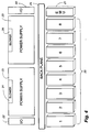
- Figure 1 provides a front view of a vertically extending cabinet 10 having four shelves, i.e. shelf-1 identified by numeral 11, shelf-2 identified by numeral 12, shelf-3 identified by numeral 13, and shelf-4 identified by numeral 14. Note that in this non-limiting example, the shelves are configured in a top-to-bottom physical/logical sequence configuration.
- FIG. 1 illustrates that cabinet 10 may include the number “M” of individual shelves, in which case a 3-shelf group “N-1", “N” and “N+1" is also provided.
- Each shelf within cabinet 10 is provided with a pair of lower-disposed and redundant input-ports or connectors 15, and a pair of upper-disposed and redundant output ports or connectors 16. Note that the two upper output ports 16 of a lower shelf, for example shelf-2 , are located closely adjacent to the two lower input ports 15 of the next adjacent shelf-3. As will be appreciated, ports 15 can also be called receiver ports, whereupon ports 16 would be called transmitter ports.
- the adjacent shelf ports 15,16 are connected by way of a short-length, 2-wire, cable 17 that prevents an inadvertent misconnection between the output port of a lower shelf and a port of another shelf.
- cables 17 are about 6 inches long.
- the top shelf is not have a cable 17 connected to its top disposed redundant pair of output ports 1.
- the construction and arrangement illustrated utilizes an analog voltage having a closely controller or precision magnitude that is received by the two input ports 15 of each shelf.
- the beginning shelf in the logical/physical sequence comprises bottom shelf-1, i.e. shelf 11, and this first shelf receives a precision-magnitude voltage from a cabinet identification (ID) box 19, by way of a conductor 18.
- ID cabinet identification
- all other shelves within the cabinet receive this required analog and precision magnitude voltage from the output port 16 of the next lower shelf by way of an above described cable 17.
- Figure 1 is of generally and identical construction and arrangement.
- Figure 2 is a top/front perspective view that shows one of the shelves, for example shelf-2 or shelf 12 of Figure 1.
- Figure 3 is a top/rear perspective view of shelf-2.
- each shelf includes eight physically individual disk drives that are individually and collectively identified as 20.
- disk drives 20 are well known dual-ported disk drives.
- Each shelf is also provided with an environmental-monitor-unit or EMU 21 that is constructed and arranged as will be described later.
- each shelf includes a redundant pair of opposite end disposed input/output (I/O) modules 22 that include the above described input/output ports 15/16.
- a redundant pair of DC power supplies 23 are also provided to supply both 5-volt and 12-volt operating power to disk drives 20, and to supply 5-volt operating power to I/O modules 22 and EMU 21.
- each shelf power supply 23 includes a cooling air blower 24, and the various components of each shelf are interconnected by way of a backplane member.
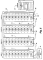
- Figure 5 provides a showing of the manner in which the four EMUs 21 of the first four shelves 11-14 (i.e., shelf-1 - shelf-4) of Figure 1 are interconnected to a host or server 30.
- a bus or cable 31 interconnects all 32 disk drives 20 to server 30.
- Bus portion 131 connects shelf-4 to shelf-5 when such an additional shelf is present in cabinet 10.
- the data processing mode of operation may take a variety of forms, as is well known in the art, and will not be described herein.
- the eight disk drives within an individual shelf may be configured as a RAID group of disk drives.
- a bus or cable 32 interconnects all four shelf EMUs 21 to server 30.
- Cable portion 132 is used to connect the EMU of shelf-4 to shelf-5 when an additional shelf-5 is present in cabinet 10.
- this reporting of a shelf address assignment error to server 30 comprises the detection by an EMU 21 that the magnitude of one of the analog/digital voltages that is used for the generation of a logical shelf address is out of an acceptable voltage range.
- This error reporting to server 30 can be called "out of band reporting".
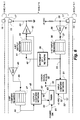
- FIG 6 is a schematic diagram that shows the construction and arrangement of a shelf EMU 21 for shelf "N" of Figure 1.
- the various shelf EMUs 21 are of generally identical construction and arrangement insofar as implementation of the present apparatus/method invention is concerned.
- the various shelf EMUs 21 perform other functions that are not related to the present invention, and these additional functions will not be described herein.
- the operation of EMUs 21 can be provided by a programmed microprocessor, by the interconnection of a number of discrete logic components, and/or by the use of an application-specific integrated circuit.
- input connector 16 of shelf “N” is provided with an analog voltage 35 whose analog magnitude comprises the decimal equivalent of the following binary value; -- (the binary address of shelf “N-1) plus (a binary one).
- -- the binary address of shelf "N-1) plus (a binary one).
- the shelf address of shelf “N-1” is decimal-5.
- the 5-bit binary address of shelf “N-1” is therefor "00101”.
- shelf "N-1” provides and output voltage 35 to shelf “N” having an magnitude that is the equivalent of binary "00110”.
- the EMU 21 that is within shelf “N-1” has operated to ensure the magnitude of analog voltage 35 comprises the correct address for shelf "N".
- An Analog-to-Digital Converter (ADC) 36 now operates to generate an digital analog voltage that is stored in 5-bit input register 38.
- the content of register 38 is the data processing address of shelf “N” that will be used when the disk drives 20 of shelf “N” are used in data processing operations. As stated, this operation can take many forms and will not be described herein.
- the 5-bit binary number now stored in register 38 is now presented to a network 39 that operates to increment the binary stored content of register 38 by a binary-1.
- the data processing address of shelf “N” has been incremented by "1”, and in this manner, the data processing address of shelf "N+1" has been generated on conductor 40.
- This next-shelf-address 40 is now stored in 5-bit output register 41 and is presented to bus or cable 44.
- a Digital to Analog Converter (DAC) 42 now operates to convert this next-shelf-address 44 into an analog voltage 43 whose magnitude is representative of the magnitude of the binary number that comprises next-shelf-address 44.
- This analog next-shelf voltage 43 is now presented to input connector 16 of shelf "N+1".
- analog voltage 43 is now presented as an input to ADC 45.
- the binary output 46 of ADC 45 is then stored in 5-bit output compare register 47.
- the stored content of register 47 should be the data processing address of next shelf "N+1".
- a digital output compare network 48 it provided with a first input that comprises the 5-bit output 49 of compare register 47 and a second input that comprises the 5-bit output 44 of output register 41. So long as these two 5-bit binary values are of the same magnitude, no error signal 50 is reported to server 30 of Figure 5 by way of bus 32. However, when the two binary values 44,49 are not of the same magnitude, this lack of matching is taken as a detection of the fact that the EMU 21 of shelf "N" has failed to generate the proper next-shelf-address for application to the input connector 16 of shelf "N+1".
- the shelf EMUs 21 advantageously operate to (1) accept a valid analog shelf address signal 35 from a prior shelf, (2) generate a digital shelf address signal 38 from the analog shelf address signal 35, (3) increment the shelf address signal 38 by "1", (4) generate an analog next-shelf-address signal 43 from the incremented signal, (5) apply this analog next-shelf-address signal 43 to the input 16 of the next shelf, (6) check to determine that the generated next-address-signal is of the correct magnitude, and (7) generate an error signal 50 when it is determined that an incorrect next-shelf-address signal 43 has been sent to the next shelf.
- an input compare network 51 receives three binary inputs, i.e. a 5-VDC or binary "11111” input 52, a ground, zero-voltage or binary "00000” input 53, and the binary output 54 of 5-bit input register 38.
- the purpose of compare network 51 is to determine if the cable-17/connector 16 input to shelf "N" is either open-circuit or short-circuit.
- input analog voltage 35 is of a zero magnitude
- comparison network 51 provides an error output 55 to server 30 by way of bus 32.
- analog input voltage 55 is equal to 5-VDC, and comparison network again provides an error output 55 to server 30.
- each shelf EMU 21 must be accomplished within a given time period, and if it is not, an error signal 50 is generated to server 30.
- a 2-second timer 60 is provided. Timer 60 is set into operation upon the detection of a power-on-event 61 for cabinet 10 (or at a time shortly thereafter), and timer 60 is reset, that is its timing operation is interrupted, by a reset signal 62 that is generated by digital compare network 48 after network 48 has operated to compare signal 49 to signal 44. In the event that timer 60 times-out before reset signal 62 is generated, then timer 60 operates to generate an error signal 63 to conductor 50 of Figure 6.
- each inter-shelf cable 17 is used only to electrically attach two physically adjacent shelves, since the shelves are mounted into cabinet 10 from the bottom up, and since the logical shelf addresses are automatically assigned in this same bottom up sequential order, the physical shelf locations within cabinet 10 map directly into the logical shelf addressing that is used for data processing purposes.
- each of the shelves 1 through M includes two sets of identical output connector 15 interconnect cable 17, input connector 16 pairs that operate as described relative to Figure 6.
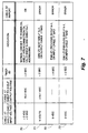
- Figure 7 is a truth table that shows the operation of the Figure 6 EMU 21. Entry 70 of this table represents the condition wherein the analog voltage 35 that is present on input cable 17 to shelf "N" is both greater-than 0 VDC and less-than 5 VDC; i.e., input voltage 35 is within a proper shelf-address analog voltage range. In addition, for condition 70 the output cable 17 that extends to shelf "N+1" contains an analog voltage level "N+1", and the 2-second timing interval of timer 60 has not expired.
- cable 32 reports "OK”, to server 30, thus indicating that a normal cabinet 10 power-on-event has occurred, that shelf "N” to shelf “N+1” interconnection is proper, that a valid shelf address has been provided to shelf "N”, and that a valid next-shelf address has been generated for shelf "N+1".
- EMU 21 that is within a shelf by a physically different but identical EMU 21. This event is called an EMU "hot swap". When this event occurs, all of the shelves that are below, and all of the shelves that are above this new-EMU shelf in the shelf sequence, will continue to report a valid shelf address.
- the EMU 21 for this new-EMU shelf now cycles or operates a valid shelf address is thereby set for this new-EMU shelf, and a valid next-shelf address is generated for the shelf that is next in sequence to the new-EMU shelf.
- Entry 71 of Figure 7 shows the operation of the Figure 6 EMU 21 for the condition where the analog voltage 35 that is present on input cable 17 to shelf "N" is again of a proper analog voltage shelf-address magnitude, indicated in Figure 7 as "n". However, in this case, the shelf's output connector/cable 115/17 that extends to the input connector 16 of shelf "N+1" contains an analog voltage that is not of the correct analog voltage level or magnitude "N+1". Again in table entry 71 the 2-second timing interval of timer 60 has not expired.
- cable 32 reports "ERROR” to server 30, thus indicating that a fault exists in that shelf's EMU 21, that the address of next shelf “N+1” was not properly generated by shelf “N”, or that a fault exists in the output connector/cable 15/17 of shelf "N".
- Entries 72 and 73 of Figure 7 are for the two fault conditions open input cable/connector 17/16 and shorted input cable/connector 17/16, respectively. In both of these conditions, and after the 2-second timing interval of timer 60 has expired, an "ERROR" message is sent to server 30 by way of bus or cable 32.
- the error message of table entries 72,73 both operate to indicate that the EMU 21 of shelf “N” is bad, that the previous shelf “N-1" did not provide a next-shelf-address to shelf “N” that was within the proper analog range "n”, or that the input cable/connector 17/16 of shelf “N” is bad.
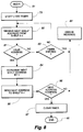
- Figure 8 is a showing of the operation of the Figure 6 the EMU 21 that is within an active shelf in flowchart form.
- the first step in this process is function 79 at which 2-second timer 60 of Figure 6 is set; i.e., the timer begins timing or counting from zero.
- Step 80 in this process is a function whereat a next-shelf address of shelf "N” is received from shelf "N-1", this being analog voltage 35 of Figure 6.
- input compare network 51 of Figure 6 checks to determine if this received next shelf address 80 is valid. If not, an error message is generated at function 82, but only after the 2-second timing period of timer 60 has expired as is indicated by the "yes" output of decision function 83.
- increment-by-one network 39 of Figure 6 operates to increase the binary value of the address of shelf "N" by one, as is shown at function 84.
- This incremented binary shelf address magnitude is then applied as an analog voltage 43 to the input connector 16 of the next shelf, i.e. to the input of shelf "N+1", as is shown at function 85.
- EMU 21 of shelf "N” now operates as shown by three entries 71,72,73 of Figure 7 to ensure that a number of errors have not occurred.
- the next address checking function is indicated in Figure 8 at decision function 86.
- the first of the conditions to be checked involves the use of Figure 6's compare network 48 to ensure that the incremented binary value 40 is the same as the binary output 46 of ADC 45, i.e. decision function 86.
- the question was the address received by shelf "N" properly increased to a value that is equal to the address of shelf N+1, is addressed.
- the second and third conditions to be checked relate to factors that include the operative condition of the cable/connector that transmits the next shelf address to shelf "N+1". If there is a short circuit or an open circuit in this cable/connector arrangement, the binary output 46 of ADC 45 will not properly compare to the binary output 40 of increment network 39.
- Timer 60 thus provides a time-supervisor feature of this invention.
- the Figure 8 function 79 operates to set 2-second timer 60 into operation.
- Decision function 83 operates to continuously monitor the state of timer 60, looking for time-out of the timer. If a time-out occurs at any time during operation of the Figure 8 process, the "yes" output of decision function 83 operates to generate error message 82. If no error is detected by Figure 8's decision function 83, then function 87 operates to reset timer 60 to zero by virtue of the "yes" output of decision function 86.
Landscapes
- Engineering & Computer Science (AREA)
- Theoretical Computer Science (AREA)
- Physics & Mathematics (AREA)
- General Engineering & Computer Science (AREA)
- General Physics & Mathematics (AREA)
- Quality & Reliability (AREA)
- Debugging And Monitoring (AREA)
- Small-Scale Networks (AREA)
- Management Or Editing Of Information On Record Carriers (AREA)
Abstract
Description
- Figure 1 is a front view of a vertically extending multi shelf cabinet in accordance with an embodiment of the invention, the cabinet having four shelves that are physically configured in a bottom-to-top sequential configuration, and wherein the cabinet is shown as being expandable to the number M of individual shelves.
- Figure 2 is a top/front perspective view that shows one of the shelves of Figure 1.
- Figure 3 is a top/rear perspective view of the shelf of Figure 2.
- Figure 4 is a top view block diagram of the Figure 2,3 shelf.
- Figure 5 provides a showing of the manner in
which the four EMUs of the first four shelves
(i.e., shelf-1 through shelf-4) of Figure 1 are
interconnected to a host or
server 30 for the purpose of digital data processing, and for the automatic shelf addressing and error monitoring purposes. - Figure 6 is a schematic circuit diagram that shows the construction and arrangement of a shelf EMU for shelf "N" of Figure 1.
- Figure 7 is a truth table that shows the operation of the Figure 6 EMU.
- Figure 8 is a showing of the operation of the Figure 6 EMU in flowchart form.
Claims (10)
- Apparatus for automatically providing a different data processing shelf address to each one of a plurality of shelves that are contained in a sequential physical order within a cabinet of a data processing system, said plurality of shelves including a shelf N, a shelf N-1 that is physically located immediately adjacent to shelf N and on a downstream side of shelf N, and a shelf N+1 that is physically located immediately adjacent to shelf N and on an upstream side of shelf N, said apparatus comprising:a shelf address output-terminal within shelf N-1 electrically connected to a shelf address input-terminal within shelf N by way of a first electrical connection, said shelf N-1 output-terminal providing a next-shelf address voltage of a given magnitude to said input-terminal of shelf N;magnitude incrementing circuitry within shelf N operable to increase said given magnitude of said next-shelf address voltage to a higher magnitude that comprises an address for shelf N+1; anda shelf address output-terminal within shelf N electrically connected to a shelf address input-terminal within shelf N+1 by way of a second electrical connection, said shelf N output-terminal providing said higher magnitude next-shelf shelf address voltage to said input-terminal within shelf N+1.
- The apparatus of claim 1 including:a supervisory timer having a timing interval;said supervisory timer being set in operation upon said shelf N-1 output-terminal receiving a next-shelf address voltage of a given magnitude to said input-terminal of shelf N, said supervisory timer being reset upon said shelf N output-terminal providing said higher magnitude next-shelf shelf address voltage to said input-terminal within shelf N+1.
- The apparatus of claim 2 including redundant said first and second electrical connections.
- The apparatus of claim 1, wherein said given magnitude of said next-shelf address voltage is normally within a valid-magnitude-range between zero and an upper-limit magnitude, and wherein said shelf-N includes:first comparing circuitry operable to compare said given magnitude of said next-shelf address voltage received by shelf N to said valid-magnitude-range, wherein said shelf N includes:second comparing circuitry operable to compare said higher magnitude next-shelf address voltage produced by said magnitude incrementing circuitry to said higher magnitude shelf address voltage applied to said input-terminal within shelf N+1 in order to determine that they are of the same magnitude.
- The apparatus of claim 4 including:fault-indicating circuitry connected to said first comparing circuitry and to said second comparing circuitry;said fault-indicating circuitry operating to indicate a fault whenever it is determined that said next-shelf voltage received by shelf N is not within said valid-magnitude-range, and whenever it is determined that said higher magnitude shelf address voltage applied to said input-terminal within shelf N+1 is not of the same magnitude as said higher magnitude next-shelf address voltage produced by said magnitude incrementing circuitry, said apparatus further including:third comparing circuitry operable to check said higher magnitude shelf address voltage applied to said input-terminal within shelf N+1 to determine that said higher magnitude shelf address voltage is within said valid-magnitude-range;said fault-indicating circuitry additionally operating to indicate a fault whenever it is determined that said higher magnitude shelf address voltage is not within said valid-magnitude-range.
- A method for automatically providing a different data processing shelf address to each one of a plurality of physically ordered shelves that are contained within a cabinet of a data processing system, said plurality of shelves including a shelf N, a shelf N-1 that is physically located immediately adjacent to shelf N and on one side of shelf N, and a shelf N+1 that is physically located immediately adjacent to shelf N and on an opposite side of shelf N, comprising the steps of:providing a shelf address output-terminal within shelf N-1;providing a shelf address input-terminal within shelf N;interconnecting said shelf address output-terminal within shelf N-1 to said shelf address input-terminal within shelf N by way of a first electrical conductor;said shelf N-1 output-terminal providing a next-shelf address voltage of a given magnitude to said input-terminal of shelf N;providing magnitude incrementing circuitry within shelf N operable to increase said given magnitude of said next-shelf address voltage to a higher magnitude that comprises an address of shelf N+1;providing a shelf address output-terminal within shelf N;providing an shelf address input-terminal within shelf N+1; andelectrically connected said shelf address output-terminal within shelf N to said shelf address input-terminal within shelf N+1 by way of a second electrical conductor to thereby provide said higher magnitude next-shelf shelf address voltage to said input-terminal within shelf N+1.
- The method of claim 6 including the step of:providing a redundant pair of said first and second electrical conductors, wherein said given magnitude of said next-shelf address voltage is normally within a valid-magnitude-range that is greater than a zero-magnitude and is less than an upper-limit magnitude, and including the step of:providing first comparing circuitry within shelf N operable to compare said given magnitude of said next-shelf address voltage received by shelf N to said valid-magnitude-range.
- The method of claim 7 including the step of:providing second comparing circuitry operable to compare said higher magnitude next-shelf address voltage produced by said magnitude incrementing circuitry to said higher magnitude shelf address voltage applied to said input-terminal within shelf N+1 in order to determine that they are of the same magnitude, further including the step of:providing fault-indicating circuitry connected to said first comparing circuitry and to said second comparing circuitry;said fault-indicating circuitry operating to indicate a fault whenever it is determined that said next-shelf voltage received by shelf N is not within said valid-magnitude-range, and whenever it is determined that said higher magnitude shelf address voltage applied to said input-terminal within shelf N+1 is not of the same magnitude as said higher magnitude next-shelf address voltage produced by said magnitude incrementing circuitry.
- The method of claim 8 including the step of:providing third comparing circuitry operable to check said higher magnitude shelf address voltage applied to said input-terminal within shelf N+1 to determine that said higher magnitude shelf address voltage is within said valid-magnitude-range;said fault-indicating circuitry additionally operating to indicate a fault whenever it is determined that said higher magnitude shelf address voltage is not within said valid-magnitude-range, further including the steps of:providing a supervisory timer that is operable to time-out at the end of a fixed timing interval; andstarting said supervisory timer when said next-shelf address voltage of a given magnitude is applied to said input-terminal of said shelf N;said fixed timing interval normally being longer than the a time interval that is necessary to complete said method;said fault-indicating circuitry additionally operating to indicate a fault whenever it is determined that said supervisory timer has timed out.
- Apparatus for automatically assigning data processing addresses to each of the integer quantity M of physically individual shelves that are within a cabinet, said M shelves being arranged in a sequential order from a first shelf-1 to a last shelf M, said sequential order providing intermediate shelves comprising shelf-2 through shelf M-1, each of said shelves having:an input-terminal adapted to receive a next-shelf address signal having an address-indicative magnitude;an output terminal adapted to transmit a next-shelf address signal having an address-indicative magnitude;a magnitude increasing network operable to step-increase the magnitude of a received next-shelf address signal to a higher magnitude, thereby generating a higher magnitude next-shelf address signal that is applied to said output-terminal;said apparatus including;a first quantity M of electrical cables;a voltage source providing a next-shelf address signal having a low magnitude that comprises a data processing address for said shelf-1;a first of said electrical cables operating to connect said voltage source to said input-terminal of said shelf-1;the quantity M-2 of said electrical cables operating to individually connect said output-terminals to said input-terminals of said shelf-2 through said shelf M-1; anda last of said electrical cables operating to connect said output-terminal of said shelf M-1 to said input-terminal of said shelf-M.
Applications Claiming Priority (2)
| Application Number | Priority Date | Filing Date | Title |
|---|---|---|---|
| US08/746,739 US5790782A (en) | 1996-11-15 | 1996-11-15 | Automatic disk drive shelf address assignment and error detection method and apparatus |
| US746739 | 1996-11-15 |
Publications (2)
| Publication Number | Publication Date |
|---|---|
| EP0843260A1 true EP0843260A1 (en) | 1998-05-20 |
| EP0843260B1 EP0843260B1 (en) | 2003-06-18 |
Family
ID=25002128
Family Applications (1)
| Application Number | Title | Priority Date | Filing Date |
|---|---|---|---|
| EP97119570A Expired - Lifetime EP0843260B1 (en) | 1996-11-15 | 1997-11-07 | Automatic shelf-address assignment for shelves containing disk drives and error detection method and apparatus |
Country Status (4)
| Country | Link |
|---|---|
| US (1) | US5790782A (en) |
| EP (1) | EP0843260B1 (en) |
| JP (1) | JPH10188528A (en) |
| DE (1) | DE69722897T2 (en) |
Cited By (5)
| Publication number | Priority date | Publication date | Assignee | Title |
|---|---|---|---|---|
| DE19860465A1 (en) * | 1998-12-28 | 2000-07-06 | Jenoptik Jena Gmbh | Method of coding functional units for performing different program routines based on installation location by storing physical parameter of functional unit such as impedance as digital address |
| FR2821453A1 (en) * | 2001-02-26 | 2002-08-30 | Valeo Climatisation | METHOD FOR IDENTIFYING THE NODES OF A COMPUTER NETWORK IN A MOTOR VEHICLE AIR CONDITIONING SYSTEM, AND AIR CONDITIONING SYSTEM APPLYING THE METHOD |
| DE10120586A1 (en) * | 2001-04-26 | 2002-11-07 | Tenovis Gmbh & Co Kg | Modular carrier device for supporting modules with unambiguous address allocation, has address allocation device combined with further similar carrier device for allocation of unambiguous address bits |
| WO2009040298A1 (en) * | 2007-09-20 | 2009-04-02 | Insta Elektro Gmbh | Method for operating a bus system, and bus system |
| CN105812504A (en) * | 2016-04-18 | 2016-07-27 | 常州格力博有限公司 | Intelligent communication address coding method |
Families Citing this family (26)
| Publication number | Priority date | Publication date | Assignee | Title |
|---|---|---|---|---|
| US5956665A (en) | 1996-11-15 | 1999-09-21 | Digital Equipment Corporation | Automatic mapping, monitoring, and control of computer room components |
| JP3222083B2 (en) * | 1997-03-21 | 2001-10-22 | 沖電気工業株式会社 | Shared memory controller |
| US6175891B1 (en) * | 1997-04-23 | 2001-01-16 | Micron Technology, Inc. | System and method for assigning addresses to memory devices |
| US6178520B1 (en) * | 1997-07-31 | 2001-01-23 | Lsi Logic Corporation | Software recognition of drive removal or insertion in a storage system |
| US6832324B2 (en) * | 2000-05-16 | 2004-12-14 | Richmount Computers Limited | Method for providing a device communicating to a backplane the current status of an associated power supply unit connected to the backplane |
| IES20010399A2 (en) * | 2000-05-16 | 2002-02-06 | Richmount Computers Ltd | A protocol for a power supply unit controller |
| IES20010398A2 (en) * | 2000-07-06 | 2002-02-06 | Richmount Computers Ltd | Improved power supply unit controller |
| IES20010400A2 (en) * | 2000-07-06 | 2002-02-06 | Richmount Computers Ltd | Data gathering device for a rack enclosure |
| IES20010396A2 (en) * | 2000-07-06 | 2002-02-06 | Richmount Computers Ltd | Fibre channel diagnostics in a storage enclosure |
| IES20010395A2 (en) * | 2000-07-26 | 2002-02-06 | Richmount Computers Ltd | Crosspoint switch for a fibre channel arbitrated loop |
| US6975590B2 (en) * | 2000-09-07 | 2005-12-13 | Eurologic Systems Limited | Fiber-channel arbitrated-loop split loop operation |
| IES20010611A2 (en) * | 2001-03-08 | 2002-09-18 | Richmount Computers Ltd | Distributed lock management chip |
| IES20010610A2 (en) * | 2001-03-08 | 2002-09-18 | Richmount Computers Ltd | Reset facility for redundant processor using a fibre channel loop |
| IES20010783A2 (en) * | 2001-04-26 | 2002-09-18 | Richmount Computers Ltd | Data storage apparatus |
| US6920511B2 (en) * | 2001-10-19 | 2005-07-19 | Hewlett-Packard Development Company, L.P. | Method and apparatus for controlling communications in data storage complexes |
| US6912599B2 (en) * | 2001-10-19 | 2005-06-28 | Hewlett-Packard Development Company, L.P. | Method and apparatus for sensing positions of device enclosures within multi-shelf cabinets |
| US7159080B1 (en) * | 2001-12-20 | 2007-01-02 | Network Appliance, Inc. | System and method for storing storage operating system data in switch ports |
| US7146522B1 (en) * | 2001-12-21 | 2006-12-05 | Network Appliance, Inc. | System and method for allocating spare disks in networked storage |
| US7296068B1 (en) | 2001-12-21 | 2007-11-13 | Network Appliance, Inc. | System and method for transfering volume ownership in net-worked storage |
| US7650412B2 (en) | 2001-12-21 | 2010-01-19 | Netapp, Inc. | Systems and method of implementing disk ownership in networked storage |
| US7089345B1 (en) | 2002-04-23 | 2006-08-08 | Adaptec, Inc. | Method and apparatus for dual porting a single port serial ATA disk drive |
| JP2004220265A (en) * | 2003-01-14 | 2004-08-05 | Fujitsu Ltd | I / O device and identification information setting method in I / O device |
| JP4045434B2 (en) * | 2003-04-23 | 2008-02-13 | 株式会社日立製作所 | Modular computer system and I/O module |
| US7111080B2 (en) * | 2004-03-01 | 2006-09-19 | Cisco Technology, Inc. | Distributing an electronic signal in a stackable device |
| US7539799B2 (en) * | 2007-02-08 | 2009-05-26 | Dot Hill Systems Corp. | Method and apparatus for identifying enclosures and devices |
| US7817036B2 (en) * | 2007-04-30 | 2010-10-19 | International Business Machines Corporation | Cabled and cableless interface method for connecting units within a rack |
Citations (5)
| Publication number | Priority date | Publication date | Assignee | Title |
|---|---|---|---|---|
| EP0162653A2 (en) * | 1984-05-22 | 1985-11-27 | Northern Telecom Limited | A bus arrangement for addressing equipment units and a method therefor |
| EP0265905A2 (en) * | 1986-10-27 | 1988-05-04 | Dieter Dr. Weiss | Addressing device for modules |
| EP0336708A2 (en) * | 1988-04-05 | 1989-10-11 | Convergent Technologies, Inc. | Modular expansion bus configuration |
| FR2641629A1 (en) * | 1989-01-11 | 1990-07-13 | Merlin Gerin | Method for automatic addressing of standard modular blocks and assembly for implementing this method |
| EP0483434A1 (en) * | 1990-10-31 | 1992-05-06 | International Business Machines Corporation | Apparatus for determining and reporting identification information relative to devices pluggable to a central unit |
Family Cites Families (8)
| Publication number | Priority date | Publication date | Assignee | Title |
|---|---|---|---|---|
| US4754397A (en) * | 1985-02-15 | 1988-06-28 | Tandem Computers Incorporated | Fault tolerant modular subsystems for computers |
| US4903194A (en) * | 1987-11-12 | 1990-02-20 | International Business Machines Corporation | Storage addressing error detection circuitry |
| US4974156A (en) * | 1988-05-05 | 1990-11-27 | International Business Machines | Multi-level peripheral data storage hierarchy with independent access to all levels of the hierarchy |
| JP2692384B2 (en) * | 1990-12-29 | 1997-12-17 | 日本電気株式会社 | Address generation circuit |
| US5555390A (en) * | 1992-10-19 | 1996-09-10 | International Business Machines Corporation | Data storage method and subsystem including a device controller for respecifying an amended start address |
| US5586250A (en) * | 1993-11-12 | 1996-12-17 | Conner Peripherals, Inc. | SCSI-coupled module for monitoring and controlling SCSI-coupled raid bank and bank environment |
| US5659698A (en) * | 1994-11-01 | 1997-08-19 | Motorola, Inc. | Method and apparatus for generating a circular buffer address in integrated circuit that performs multiple communications tasks |
| US5586253A (en) * | 1994-12-15 | 1996-12-17 | Stratus Computer | Method and apparatus for validating I/O addresses in a fault-tolerant computer system |
-
1996
- 1996-11-15 US US08/746,739 patent/US5790782A/en not_active Expired - Lifetime
-
1997
- 1997-11-07 DE DE69722897T patent/DE69722897T2/en not_active Expired - Lifetime
- 1997-11-07 EP EP97119570A patent/EP0843260B1/en not_active Expired - Lifetime
- 1997-11-11 JP JP9308397A patent/JPH10188528A/en active Pending
Patent Citations (5)
| Publication number | Priority date | Publication date | Assignee | Title |
|---|---|---|---|---|
| EP0162653A2 (en) * | 1984-05-22 | 1985-11-27 | Northern Telecom Limited | A bus arrangement for addressing equipment units and a method therefor |
| EP0265905A2 (en) * | 1986-10-27 | 1988-05-04 | Dieter Dr. Weiss | Addressing device for modules |
| EP0336708A2 (en) * | 1988-04-05 | 1989-10-11 | Convergent Technologies, Inc. | Modular expansion bus configuration |
| FR2641629A1 (en) * | 1989-01-11 | 1990-07-13 | Merlin Gerin | Method for automatic addressing of standard modular blocks and assembly for implementing this method |
| EP0483434A1 (en) * | 1990-10-31 | 1992-05-06 | International Business Machines Corporation | Apparatus for determining and reporting identification information relative to devices pluggable to a central unit |
Cited By (10)
| Publication number | Priority date | Publication date | Assignee | Title |
|---|---|---|---|---|
| DE19860465A1 (en) * | 1998-12-28 | 2000-07-06 | Jenoptik Jena Gmbh | Method of coding functional units for performing different program routines based on installation location by storing physical parameter of functional unit such as impedance as digital address |
| FR2821453A1 (en) * | 2001-02-26 | 2002-08-30 | Valeo Climatisation | METHOD FOR IDENTIFYING THE NODES OF A COMPUTER NETWORK IN A MOTOR VEHICLE AIR CONDITIONING SYSTEM, AND AIR CONDITIONING SYSTEM APPLYING THE METHOD |
| WO2002069149A1 (en) * | 2001-02-26 | 2002-09-06 | Valeo Climatisation | Method for identifying nodes in a computer network in a motor vehicle air conditioning installation |
| US7869918B2 (en) | 2001-02-26 | 2011-01-11 | Valeo Climatisation | Method of identifying nodes in a computer network in a motor vehicle air conditioning installation |
| US8554405B2 (en) | 2001-02-26 | 2013-10-08 | Valeo Systemes Thermiques | Method of identification of the nodes of a computer network in an air conditioning installation of a motor vehicle, and air conditioning installation using the method |
| DE10120586A1 (en) * | 2001-04-26 | 2002-11-07 | Tenovis Gmbh & Co Kg | Modular carrier device for supporting modules with unambiguous address allocation, has address allocation device combined with further similar carrier device for allocation of unambiguous address bits |
| DE10120586B4 (en) * | 2001-04-26 | 2010-09-30 | Tenovis Gmbh & Co. Kg | Modular carrier device for carrying assemblies with unique address assignment |
| WO2009040298A1 (en) * | 2007-09-20 | 2009-04-02 | Insta Elektro Gmbh | Method for operating a bus system, and bus system |
| CN105812504A (en) * | 2016-04-18 | 2016-07-27 | 常州格力博有限公司 | Intelligent communication address coding method |
| CN105812504B (en) * | 2016-04-18 | 2019-03-19 | 常州格力博有限公司 | A kind of intelligent mailing address coding method |
Also Published As
| Publication number | Publication date |
|---|---|
| EP0843260B1 (en) | 2003-06-18 |
| JPH10188528A (en) | 1998-07-21 |
| DE69722897T2 (en) | 2004-05-19 |
| US5790782A (en) | 1998-08-04 |
| DE69722897D1 (en) | 2003-07-24 |
Similar Documents
| Publication | Publication Date | Title |
|---|---|---|
| US5790782A (en) | Automatic disk drive shelf address assignment and error detection method and apparatus | |
| EP0204507B1 (en) | System configuration tracing method and apparatus | |
| US5414343A (en) | Permanently installed cable system with integrated multi-cable tester | |
| EP1008943B1 (en) | Cascade connection of communicating devices | |
| US5065141A (en) | Expanded register rack for a programmable logic controller | |
| US5148389A (en) | Modular expansion bus configuration | |
| US5892973A (en) | System and method for determining attributes and coupling characteristics of components by comparatively observing provided reference signal | |
| EP0148759A2 (en) | Programmable digital signal testing system | |
| WO2020134340A1 (en) | Hard drive extension system and electronic device | |
| CN111176913A (en) | Circuit and method for detecting Cable Port in server | |
| EP0632280A2 (en) | Inter-section cross cable detection system | |
| US4918693A (en) | Apparatus for physically locating faulty electrical components | |
| US4042832A (en) | Logic board interlock indication apparatus | |
| US7113003B2 (en) | Presence indication signal associated with an attachment | |
| JP3588936B2 (en) | Flexible high-speed multiplexed remote input / output system | |
| US5245331A (en) | Multiple adapter response detection circuit | |
| EP1232440A2 (en) | FAULT TOLERANT VIRTUAL VMEbus BACKPLANE DESIGN | |
| CN117692354A (en) | A cable detection method and computing device | |
| KR20060061359A (en) | Data block transmission method and apparatus | |
| US6642733B1 (en) | Apparatus for indentifying defects in electronic assemblies | |
| US6553519B1 (en) | Method for detecting signal transfer errors in near real time in a digital system | |
| JP2830486B2 (en) | Communication device | |
| CN120200947A (en) | Test systems and equipment | |
| JPS58108856A (en) | Signal separation control system of terminal controller | |
| JPS6041845A (en) | Line connecting system |
Legal Events
| Date | Code | Title | Description |
|---|---|---|---|
| PUAI | Public reference made under article 153(3) epc to a published international application that has entered the european phase |
Free format text: ORIGINAL CODE: 0009012 |
|
| AK | Designated contracting states |
Kind code of ref document: A1 Designated state(s): DE FR GB IT |
|
| AX | Request for extension of the european patent |
Free format text: AL;LT;LV;MK;RO;SI |
|
| 17P | Request for examination filed |
Effective date: 19980720 |
|
| AKX | Designation fees paid |
Free format text: DE FR GB IT |
|
| RBV | Designated contracting states (corrected) |
Designated state(s): DE FR GB IT |
|
| RAP1 | Party data changed (applicant data changed or rights of an application transferred) |
Owner name: COMPAQ COMPUTER CORPORATION |
|
| 17Q | First examination report despatched |
Effective date: 20011127 |
|
| GRAH | Despatch of communication of intention to grant a patent |
Free format text: ORIGINAL CODE: EPIDOS IGRA |
|
| RIN1 | Information on inventor provided before grant (corrected) |
Inventor name: LIEBER, TIMOTHY Inventor name: MARTINEZ, REUBEN |
|
| GRAH | Despatch of communication of intention to grant a patent |
Free format text: ORIGINAL CODE: EPIDOS IGRA |
|
| GRAA | (expected) grant |
Free format text: ORIGINAL CODE: 0009210 |
|
| AK | Designated contracting states |
Designated state(s): DE FR GB IT |
|
| PG25 | Lapsed in a contracting state [announced via postgrant information from national office to epo] |
Ref country code: IT Free format text: LAPSE BECAUSE OF FAILURE TO SUBMIT A TRANSLATION OF THE DESCRIPTION OR TO PAY THE FEE WITHIN THE PRESCRIBED TIME-LIMIT;WARNING: LAPSES OF ITALIAN PATENTS WITH EFFECTIVE DATE BEFORE 2007 MAY HAVE OCCURRED AT ANY TIME BEFORE 2007. THE CORRECT EFFECTIVE DATE MAY BE DIFFERENT FROM THE ONE RECORDED. Effective date: 20030618 |
|
| REG | Reference to a national code |
Ref country code: GB Ref legal event code: FG4D |
|
| REF | Corresponds to: |
Ref document number: 69722897 Country of ref document: DE Date of ref document: 20030724 Kind code of ref document: P |
|
| ET | Fr: translation filed | ||
| PLBE | No opposition filed within time limit |
Free format text: ORIGINAL CODE: 0009261 |
|
| STAA | Information on the status of an ep patent application or granted ep patent |
Free format text: STATUS: NO OPPOSITION FILED WITHIN TIME LIMIT |
|
| 26N | No opposition filed |
Effective date: 20040319 |
|
| REG | Reference to a national code |
Ref country code: GB Ref legal event code: 732E |
|
| PGFP | Annual fee paid to national office [announced via postgrant information from national office to epo] |
Ref country code: FR Payment date: 20091201 Year of fee payment: 13 |
|
| REG | Reference to a national code |
Ref country code: FR Ref legal event code: ST Effective date: 20110801 |
|
| PG25 | Lapsed in a contracting state [announced via postgrant information from national office to epo] |
Ref country code: FR Free format text: LAPSE BECAUSE OF NON-PAYMENT OF DUE FEES Effective date: 20101130 |
|
| REG | Reference to a national code |
Ref country code: DE Ref legal event code: R082 Ref document number: 69722897 Country of ref document: DE Representative=s name: BOEHMERT & BOEHMERT ANWALTSPARTNERSCHAFT MBB -, DE Effective date: 20120329 Ref country code: DE Ref legal event code: R081 Ref document number: 69722897 Country of ref document: DE Owner name: HEWLETT-PACKARD DEVELOPMENT COMPANY, L.P., HOU, US Free format text: FORMER OWNER: COMPAQ COMPUTER CORP., HOUSTON, TEX., US Effective date: 20120329 |
|
| PGFP | Annual fee paid to national office [announced via postgrant information from national office to epo] |
Ref country code: DE Payment date: 20121128 Year of fee payment: 16 |
|
| PGFP | Annual fee paid to national office [announced via postgrant information from national office to epo] |
Ref country code: GB Payment date: 20121126 Year of fee payment: 16 |
|
| GBPC | Gb: european patent ceased through non-payment of renewal fee |
Effective date: 20131107 |
|
| REG | Reference to a national code |
Ref country code: DE Ref legal event code: R119 Ref document number: 69722897 Country of ref document: DE Effective date: 20140603 |
|
| PG25 | Lapsed in a contracting state [announced via postgrant information from national office to epo] |
Ref country code: DE Free format text: LAPSE BECAUSE OF NON-PAYMENT OF DUE FEES Effective date: 20140603 |
|
| PG25 | Lapsed in a contracting state [announced via postgrant information from national office to epo] |
Ref country code: GB Free format text: LAPSE BECAUSE OF NON-PAYMENT OF DUE FEES Effective date: 20131107 |