EP0162653A2 - A bus arrangement for addressing equipment units and a method therefor - Google Patents
A bus arrangement for addressing equipment units and a method therefor Download PDFInfo
- Publication number
- EP0162653A2 EP0162653A2 EP85303389A EP85303389A EP0162653A2 EP 0162653 A2 EP0162653 A2 EP 0162653A2 EP 85303389 A EP85303389 A EP 85303389A EP 85303389 A EP85303389 A EP 85303389A EP 0162653 A2 EP0162653 A2 EP 0162653A2
- Authority
- EP
- European Patent Office
- Prior art keywords
- bus
- address
- unit
- rack
- arrangement
- Prior art date
- Legal status (The legal status is an assumption and is not a legal conclusion. Google has not performed a legal analysis and makes no representation as to the accuracy of the status listed.)
- Withdrawn
Links
- 238000000034 method Methods 0.000 title claims description 8
- 230000001419 dependent effect Effects 0.000 claims description 3
- 238000010079 rubber tapping Methods 0.000 claims 1
- 230000003068 static effect Effects 0.000 claims 1
- 230000008520 organization Effects 0.000 abstract description 2
- 230000004048 modification Effects 0.000 abstract 1
- 238000012986 modification Methods 0.000 abstract 1
Images


Classifications
-
- G—PHYSICS
- G06—COMPUTING; CALCULATING OR COUNTING
- G06F—ELECTRIC DIGITAL DATA PROCESSING
- G06F12/00—Accessing, addressing or allocating within memory systems or architectures
- G06F12/02—Addressing or allocation; Relocation
- G06F12/06—Addressing a physical block of locations, e.g. base addressing, module addressing, memory dedication
- G06F12/0646—Configuration or reconfiguration
- G06F12/0669—Configuration or reconfiguration with decentralised address assignment
- G06F12/0676—Configuration or reconfiguration with decentralised address assignment the address being position dependent
-
- G06T3/02—
Definitions
- This invention relates generally to a bus arrangement for providing equipment units with an address and more particularly to a a bus arrangement wherein each individual unit achieves its address automatically according to its relative physical position within the organization of the equipment units without the need for setting any switches (or the like).
- the present invention is directed to automatically providing an address for each equipment unit as it is connected to other equipment units and thereby reducing the chance of operator error.
- the present invention employs a unique addressing bus.
- This unique addressing bus is the same in each equipment unit.
- the input side (entry port) of the address bus receives signals from an adjacent equipment unit and transfers these signals to an output termination (exit port).
- the address bus is modified such that one input lead becomes terminated and a ground lead is picked up. This will be explained in more detail in the figures accompanying this description.
- the present invention is a bus arrangement for interconnecting a plurality of equipment units in such a fashion that each unit is given a unique address, dependent solely upon its relative position to other equipment units in the interconnection, the bus arrangement in each unit comprising: an entry port having N terminals, N being a positive integer equal to or greater than two; an exit port having N terminals corresponding respectively to the N terminals of the entry port, wherein the 2nd to N th terminals s of the entry port are connected to the ist to (N-1) th terminals, respectively, of the exit port, and an originating connection is made to the N th terminal of the exit port.
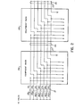
- FIG. 1 depicts eight equipment racks 10a through 10h and referred to collectively as equipment racks (or equipment units) 10.
- Equipment racks 10a through 10h are interconnected with buses llb through llh respectively as shown in Figure 1.
- Buses 11b through llh are referred to collectively as buses 11 and are identical one with another.
- Bus 12 applies the initial address bus to rack 10a as shown.
- each equipment rack 10 receives its address according to its position relative to bus 12; that is, rack 10a achieves a particular address because it is the rack that receives bus 12.
- Equipment rack 10b receives its address because it is the one connected to rack 10a.
- rack 10c achieves its address solely due to the fact that it is the one connected to rack 10b etc., all the way through to 10h. This is shown in more detail in Figure 2 to which attention is directed.
- Bus 12 is comprised of leads 13, 14, 15, 16, 17, 18 and 19 as depicted in Figure 2 and are connected to a plus five volt supply via resistors 13a, 14a, 15a, 16a, 17a, 18a, and 19a respectively (note: each resistor 13a to 19a inclusive is 5.1 Kohms).
- the address of equipment rack 10a is given in the bottom of the block as A B C D E F G which of course in this illustrative embodiment is logic 1111111. It will also be noted that after the address of equipment rack 10a is established, lead 13 terminates. It will also be noted that leads 14 through 19 continue through equipment rack 10a and are shifted up one place position such that when they cross to equipment rack 10b, via bus 11b, their position is one above what it was when it entered equipment rack 10a, and in addition a new lead (a ground lead) indicated as lead 21 is added. This provides an address for equipment rack 10b, once again of A B C D E F G which is now logic 1111110.
- each equipment rack 10 receives a unique address dependent only upon its physical position within the assembly of racks.
- the seven bit binary number used to address the racks may prove to be somewhat cumbersome.
- an encoding scheme may be used to reduce the address to a three digit binary number within a rack 10 itself.
- This encoding scheme is implemented by an 8-line to 3-line encoder such as a model SN74LS148.
- the end result of this encoding scheme is depicted in Table I wherein there is shown both an unencoded address for each equipment rack 10 as well as an encoded address.
- equipment rack 10a has an unencoded address of 1 1 1 1 1 1 1 and an encoded address of 1 1 1. Similar results for the other racks 10 can be found in Table I.
- Each rack 10 may be subdivided into eight slots. These eight slots are represented in Figure 3 with the four slots running from left to right on the top of rack 10a, being indicated as slots 1 through 4 and the four slots on thf bottom of rack 10a being indicated as 5 through 8. When addressing, these slots can each have a unique address; for example, a three digit tinary number running from 0 0 0 to 1 1 1. This would of course necessitate three additional lines on the address buses llb and lie etc., shown in Figures 1 and 2.
- Table II Attention is directed to Table II wherein there are depicted the unencoded addresses and the encoded addresses for the racks 10 when the slot numbers are als taken into account. As can be seen from Table II, the last three digits of each address (encoded or unencoded) is the slot address.
- Figure 4 depicts a further arrangement of three equipment racks 30a, 30b, and 30c referred to collectively as racks 30.
- the principle of operation is the same as the Figure 2 embodiment.
- the interconnecting buses i.e. buses 31b and 31c
- input bus 32 have only two leads.
- addresses can be provided; namely logic 11, logic 10, and logic 00.
- rack 30a achieves an address of logic 11
- rack 30b achieves an address of logic 10
- rack 30c achieves an address of logic 00.
- Input bus 32 is connected to a plus five volt supply via 5.1 Kohm resistors 33a and 33b.
- Figure 5 is similar to Figure 4 except that input bus 42 is logic 0 (i.e. grouid, instead of plus five volts). Consequently, the address of rack 40a is logic 00. Interconnecting bus 41b joins racks 40a and 40b, and interconnecting bus 41c joins racks 40b and 40c. The address of rack 40b is logic 01 since one lead of bus 41b applies plus five volts from resistor 43a. The address of rack 40c is logic 11 since now both leads of bus 41c carry plus five volts (from resistors 43a and 43b).
Abstract
Description
- This invention relates generally to a bus arrangement for providing equipment units with an address and more particularly to a a bus arrangement wherein each individual unit achieves its address automatically according to its relative physical position within the organization of the equipment units without the need for setting any switches (or the like).
- It is common practice, when installing equipment, to give each equipment unit an address. In this manner, each individual unit can be uniquely addressed and controlled independently of the other equipment units. In the past this addressing has been achieved by the use of small switches, for example DIP switches, on each equipment unit. A unique address is then given to each equipment unit by setting the switches to appropriate positions. As would be expected, this method of setting the addresses for the various equipment units is both time consuming and prone to operator error.
- The present invention is directed to automatically providing an address for each equipment unit as it is connected to other equipment units and thereby reducing the chance of operator error.
- More specifically, the present invention employs a unique addressing bus. This unique addressing bus is the same in each equipment unit. The input side (entry port) of the address bus receives signals from an adjacent equipment unit and transfers these signals to an output termination (exit port). In the process of doing this, the address bus is modified such that one input lead becomes terminated and a ground lead is picked up. This will be explained in more detail in the figures accompanying this description.
- Stated in other terms, the present invention is a bus arrangement for interconnecting a plurality of equipment units in such a fashion that each unit is given a unique address, dependent solely upon its relative position to other equipment units in the interconnection, the bus arrangement in each unit comprising: an entry port having N terminals, N being a positive integer equal to or greater than two; an exit port having N terminals corresponding respectively to the N terminals of the entry port, wherein the 2nd to Nth terminals s of the entry port are connected to the ist to (N-1)th terminals, respectively, of the exit port, and an originating connection is made to the Nth terminal of the exit port.
- The present invention will now be described in more detail with reference to the accompanying drawings wherein like parts in each of the several figures are identified by the same reference character, and wherein:
- Figure 1 depicts eight equipment units or racks interconnected according to the present invention;
- Figure 2 depicts two equipment racks from Figure 1 shown with their addressing bus in more detail;
- Figure 3 depicts the arrangement of slots within one of these equipment units or racks;
- Figure 4 depicts a first variation of the Figure 1 embodiment; and
- Figure 5 depicts a second variation of the Figure 1 embodiment.
- Figure 1 depicts eight equipment racks 10a through 10h and referred to collectively as equipment racks (or equipment units) 10. Equipment racks 10a through 10h are interconnected with buses llb through llh respectively as shown in Figure 1. Buses 11b through llh are referred to collectively as buses 11 and are identical one with another.
Bus 12 applies the initial address bus torack 10a as shown. It should be noted in Figure 1 that each equipment rack 10 receives its address according to its position relative tobus 12; that is,rack 10a achieves a particular address because it is the rack that receivesbus 12. Equipment rack 10b receives its address because it is the one connected torack 10a. Similarly, rack 10c achieves its address solely due to the fact that it is the one connected to rack 10b etc., all the way through to 10h. This is shown in more detail in Figure 2 to which attention is directed. - In Figure 2, only
racks 10a and 10b are depicted. The remaining racks are of course interconnected in an analagous fashion.Bus 12 is comprised of leads 13, 14, 15, 16, 17, 18 and 19 as depicted in Figure 2 and are connected to a plus five volt supply via resistors 13a, 14a, 15a, 16a, 17a, 18a, and 19a respectively (note: each resistor 13a to 19a inclusive is 5.1 Kohms). - As depicted in Figure 2, the address of
equipment rack 10a is given in the bottom of the block as A B C D E F G which of course in this illustrative embodiment is logic 1111111. It will also be noted that after the address ofequipment rack 10a is established, lead 13 terminates. It will also be noted that leads 14 through 19 continue throughequipment rack 10a and are shifted up one place position such that when they cross to equipment rack 10b, via bus 11b, their position is one above what it was when it enteredequipment rack 10a, and in addition a new lead (a ground lead) indicated aslead 21 is added. This provides an address for equipment rack 10b, once again of A B C D E F G which is now logic 1111110. Once again, as the leads are shifted out of equipment rack 10b, via bus 11c, we see that they are once again shifted up with the uppermost lead being dropped and anew ground lead 22 being added. Consequently, the address of equipment unit 10c, not shown in Figure 2, will be logic 1111100 (etc., for the remaining equipment units). These addresses (unencoded) are depicted in more detail in Table 1 to which attention is directed.
- Consequently, it can be seen that the first rack (i.e.
rack 10a) has the address of all logic ls. Rack 10b, immediately to its right, has the address of all logic is followed by asingle logic 0. The next rack (i.e. rack 10c) has the address of five logic Is followed by two logic Os; etc., until we come to rack 10h which has an address of all logic Os. In this manner each equipment rack 10 receives a unique address dependent only upon its physical position within the assembly of racks. - As may be appreciated, the seven bit binary number used to address the racks may prove to be somewhat cumbersome. To simplify this address, an encoding scheme may be used to reduce the address to a three digit binary number within a rack 10 itself. This encoding scheme is implemented by an 8-line to 3-line encoder such as a model SN74LS148. The end result of this encoding scheme is depicted in Table I wherein there is shown both an unencoded address for each equipment rack 10 as well as an encoded address. For example,
equipment rack 10a has an unencoded address of 1 1 1 1 1 1 1 and an encoded address of 1 1 1. Similar results for the other racks 10 can be found in Table I. - Each rack 10 may be subdivided into eight slots. These eight slots are represented in Figure 3 with the four slots running from left to right on the top of
rack 10a, being indicated as slots 1 through 4 and the four slots on thf bottom ofrack 10a being indicated as 5 through 8. When addressing, these slots can each have a unique address; for example, a three digit tinary number running from 0 0 0 to 1 1 1. This would of course necessitate three additional lines on the address buses llb and lie etc., shown in Figures 1 and 2. - Attention is directed to Table II wherein there are depicted the unencoded addresses and the encoded addresses for the racks 10 when the slot numbers are als taken into account. As can be seen from Table II, the last three digits of each address (encoded or unencoded) is the slot address.


- Figure 4 depicts a further arrangement of three equipment racks 30a, 30b, and 30c referred to collectively as racks 30. The principle of operation is the same as the Figure 2 embodiment. The difference is that the interconnecting buses (i.e. buses 31b and 31c) along with
input bus 32 have only two leads. As a result, only three addresses can be provided; namely logic 11, logic 10, and logic 00. - As shown in Figure 4, rack 30a achieves an address of logic 11,
rack 30b achieves an address of logic 10, and rack 30c achieves an address of logic 00.Input bus 32 is connected to a plus five volt supply via 5.1 Kohmresistors 33a and 33b. - Figure 5 is similar to Figure 4 except that
input bus 42 is logic 0 (i.e. grouid, instead of plus five volts). Consequently, the address of rack 40a is logic 00. Interconnecting bus 41b joins racks 40a and 40b, and interconnecting bus 41c joins racks 40b and 40c. The address of rack 40b is logic 01 since one lead of bus 41b applies plus five volts from resistor 43a. The address of rack 40c is logic 11 since now both leads of bus 41c carry plus five volts (fromresistors 43a and 43b).
Claims (11)
Applications Claiming Priority (2)
| Application Number | Priority Date | Filing Date | Title |
|---|---|---|---|
| US06/613,062 US4626846A (en) | 1984-05-22 | 1984-05-22 | Bus arrangement for addressing equipment units and a method therefor |
| US613062 | 2003-07-03 |
Publications (2)
| Publication Number | Publication Date |
|---|---|
| EP0162653A2 true EP0162653A2 (en) | 1985-11-27 |
| EP0162653A3 EP0162653A3 (en) | 1988-07-20 |
Family
ID=24455713
Family Applications (1)
| Application Number | Title | Priority Date | Filing Date |
|---|---|---|---|
| EP85303389A Withdrawn EP0162653A3 (en) | 1984-05-22 | 1985-05-14 | A bus arrangement for addressing equipment units and a method therefor |
Country Status (5)
| Country | Link |
|---|---|
| US (1) | US4626846A (en) |
| EP (1) | EP0162653A3 (en) |
| JP (1) | JPS60254265A (en) |
| KR (1) | KR850008062A (en) |
| CA (1) | CA1220831A (en) |
Cited By (3)
| Publication number | Priority date | Publication date | Assignee | Title |
|---|---|---|---|---|
| EP0340325A1 (en) * | 1988-05-05 | 1989-11-08 | Hewlett-Packard GmbH | Digitally addressable electronic device |
| EP0843260A1 (en) * | 1996-11-15 | 1998-05-20 | Digital Equipment Corporation | Automatic shelf-address assignment for shelves containing disk drives and error detection method and apparatus |
| WO2010127917A1 (en) * | 2009-05-06 | 2010-11-11 | Robert Bosch Gmbh | Sensor system and method for operating a sensor system |
Families Citing this family (25)
| Publication number | Priority date | Publication date | Assignee | Title |
|---|---|---|---|---|
| US4689786A (en) * | 1985-03-21 | 1987-08-25 | Apple Computer, Inc. | Local area network with self assigned address method |
| US4910655A (en) * | 1985-08-14 | 1990-03-20 | Apple Computer, Inc. | Apparatus for transferring signals and data under the control of a host computer |
| US4875158A (en) * | 1985-08-14 | 1989-10-17 | Apple Computer, Inc. | Method for requesting service by a device which generates a service request signal successively until it is serviced |
| US4918598A (en) * | 1985-08-14 | 1990-04-17 | Apple Computer, Inc. | Method for selectively activating and deactivating devices having same first address and different extended addresses |
| US4912627A (en) * | 1985-08-14 | 1990-03-27 | Apple Computer, Inc. | Method for storing a second number as a command address of a first peripheral device and a third number as a command address of a second peripheral device |
| US4811275A (en) * | 1986-05-28 | 1989-03-07 | Unisys Corporation | Addressing system for an expandable modular electromechanical memory assembly |
| US5539390A (en) * | 1990-07-19 | 1996-07-23 | Sony Corporation | Method for setting addresses for series-connectd apparatuses |
| US5204669A (en) * | 1990-08-30 | 1993-04-20 | Datacard Corporation | Automatic station identification where function modules automatically initialize |
| US5210531A (en) * | 1991-03-02 | 1993-05-11 | Fordham Richard J | Monitoring and control system with binary addressing |
| US5160276A (en) * | 1991-07-09 | 1992-11-03 | Group Dekko International | Modular communication interconnection system |
| NL9102198A (en) * | 1991-12-31 | 1993-07-16 | Hadewe Bv | METHOD FOR CONTROLLING A POST COMPOSITION DEVICE, EQUIPMENT AND DEVICES FOR APPLYING THAT METHOD |
| JP2963812B2 (en) * | 1992-02-27 | 1999-10-18 | 富士通株式会社 | Automatic identification number setting circuit card mounting shelf device |
| US5719933A (en) * | 1994-02-18 | 1998-02-17 | Welch; Richard | Wiring arrangement for a communication interconnection system |
| US5613158A (en) * | 1994-05-25 | 1997-03-18 | Tandem Computers, Inc. | System for specifying addresses by creating a multi-bit ranked ordered anchor pattern and creating next address by shifting in the direction of the superior position |
| US5576698A (en) * | 1994-09-22 | 1996-11-19 | Unisys Corporation | Physical addressing of modules |
| US5629685A (en) * | 1995-02-23 | 1997-05-13 | International Business Machines Corporation | Segmentable addressable modular communication network hubs |
| US5680113A (en) * | 1995-02-24 | 1997-10-21 | International Business Machines Corporation | Dynamic address assignments to serially connected devices |
| US6537109B1 (en) * | 1997-01-16 | 2003-03-25 | Hewlett-Packard Company | Chainable I/O termination block system |
| US6174196B1 (en) * | 1998-09-30 | 2001-01-16 | Lucent Technologies Inc. | Low-cost multi-shelf cabling arrangement |
| US6795871B2 (en) | 2000-12-22 | 2004-09-21 | General Electric Company | Appliance sensor and man machine interface bus |
| JP4794218B2 (en) * | 2004-06-25 | 2011-10-19 | パナソニック株式会社 | Slave device, master device and stacking device |
| US20060061493A1 (en) * | 2004-09-22 | 2006-03-23 | Larson Lee A | Apparatus and method for assigning circuit card base addresses using thermometer codes |
| US8325010B2 (en) * | 2010-02-05 | 2012-12-04 | Emerson Electric Co. | Physical addressing for transient voltage surge suppressor modules |
| US9217995B2 (en) * | 2012-07-23 | 2015-12-22 | Brian W. Karam | Entertainment, lighting and climate control system |
| CN103176418B (en) * | 2013-03-08 | 2015-08-19 | 深圳市泰昂能源科技股份有限公司 | The address coding method of Power System Intelligent feeder switch module |
Citations (2)
| Publication number | Priority date | Publication date | Assignee | Title |
|---|---|---|---|---|
| FR2245028A1 (en) * | 1973-09-24 | 1975-04-18 | Siemens Ag | |
| US4443866A (en) * | 1975-08-27 | 1984-04-17 | Corning Glass Works | Automatic device selection circuit |
Family Cites Families (2)
| Publication number | Priority date | Publication date | Assignee | Title |
|---|---|---|---|---|
| US4016369A (en) * | 1976-03-09 | 1977-04-05 | Bell Telephone Laboratories, Incorporated | Addressing arrangements for communications networks |
| US4253087A (en) * | 1979-03-08 | 1981-02-24 | Nestar Systems Incorporated | Self-assigning address system |
-
1984
- 1984-05-22 US US06/613,062 patent/US4626846A/en not_active Expired - Fee Related
- 1984-08-30 CA CA000462095A patent/CA1220831A/en not_active Expired
-
1985
- 1985-05-14 EP EP85303389A patent/EP0162653A3/en not_active Withdrawn
- 1985-05-20 KR KR1019850003444A patent/KR850008062A/en not_active Application Discontinuation
- 1985-05-21 JP JP60107080A patent/JPS60254265A/en active Pending
Patent Citations (2)
| Publication number | Priority date | Publication date | Assignee | Title |
|---|---|---|---|---|
| FR2245028A1 (en) * | 1973-09-24 | 1975-04-18 | Siemens Ag | |
| US4443866A (en) * | 1975-08-27 | 1984-04-17 | Corning Glass Works | Automatic device selection circuit |
Non-Patent Citations (1)
| Title |
|---|
| IBM TECHNICAL DISCLOSURE BULLETIN, vol. 22, no. 3, August 1979, pages 1124-1127, New York, US; D. MELTZER: "Selective addressing of devices using primitive polynomial transformations" * |
Cited By (3)
| Publication number | Priority date | Publication date | Assignee | Title |
|---|---|---|---|---|
| EP0340325A1 (en) * | 1988-05-05 | 1989-11-08 | Hewlett-Packard GmbH | Digitally addressable electronic device |
| EP0843260A1 (en) * | 1996-11-15 | 1998-05-20 | Digital Equipment Corporation | Automatic shelf-address assignment for shelves containing disk drives and error detection method and apparatus |
| WO2010127917A1 (en) * | 2009-05-06 | 2010-11-11 | Robert Bosch Gmbh | Sensor system and method for operating a sensor system |
Also Published As
| Publication number | Publication date |
|---|---|
| EP0162653A3 (en) | 1988-07-20 |
| US4626846A (en) | 1986-12-02 |
| CA1220831A (en) | 1987-04-21 |
| KR850008062A (en) | 1985-12-11 |
| JPS60254265A (en) | 1985-12-14 |
Similar Documents
| Publication | Publication Date | Title |
|---|---|---|
| EP0162653A2 (en) | A bus arrangement for addressing equipment units and a method therefor | |
| US5148389A (en) | Modular expansion bus configuration | |
| US5293489A (en) | Circuit arrangement capable of centralizing control of a switching network | |
| US3872452A (en) | Floating addressing system and method | |
| US5613158A (en) | System for specifying addresses by creating a multi-bit ranked ordered anchor pattern and creating next address by shifting in the direction of the superior position | |
| US4429414A (en) | Pattern recognition system operating by the multiple similarity method | |
| US4701746A (en) | Device for converting code signals of one bit number into a code signal of a smaller bit number | |
| US5153843A (en) | Layout of large multistage interconnection networks technical field | |
| ES8704063A1 (en) | Routing address bit selection in a packet switching network | |
| US4349702A (en) | Nodal switching network with binary order links | |
| US4651301A (en) | Circuit arrangement for performing rapid sortation or selection according to rank | |
| US5786777A (en) | Data compression communication method between a main control unit and terminals | |
| US4733216A (en) | N+1 bit resolution from an N bit A/D converter | |
| US3993980A (en) | System for hard wiring information into integrated circuit elements | |
| US6516377B1 (en) | Self-configuring modular electronic system | |
| CA2090567A1 (en) | Method of and apparatus for data distribution | |
| DE19701508C2 (en) | Self-configuring modular electronic system, especially computer system | |
| CA1101971A (en) | Trunk control system | |
| US4327418A (en) | High speed information selection and transfer system | |
| EP0322075A3 (en) | Switching network and controller for a switching system | |
| EP0562704B1 (en) | Microprocessor controlled apparatus | |
| US4015244A (en) | Selective addressing system | |
| US3568159A (en) | Multimatch processing system | |
| US4132866A (en) | Concentration network for a time division multiplex telephone exchange with pulse amplitude modulation | |
| SU1472949A1 (en) | Programmable logic matrix |
Legal Events
| Date | Code | Title | Description |
|---|---|---|---|
| PUAI | Public reference made under article 153(3) epc to a published international application that has entered the european phase |
Free format text: ORIGINAL CODE: 0009012 |
|
| AK | Designated contracting states |
Designated state(s): AT DE FR GB IT NL |
|
| PUAL | Search report despatched |
Free format text: ORIGINAL CODE: 0009013 |
|
| AK | Designated contracting states |
Kind code of ref document: A3 Designated state(s): AT DE FR GB IT NL |
|
| 17P | Request for examination filed |
Effective date: 19890120 |
|
| 17Q | First examination report despatched |
Effective date: 19900705 |
|
| STAA | Information on the status of an ep patent application or granted ep patent |
Free format text: STATUS: THE APPLICATION IS DEEMED TO BE WITHDRAWN |
|
| 18D | Application deemed to be withdrawn |
Effective date: 19901116 |
|
| RIN1 | Information on inventor provided before grant (corrected) |
Inventor name: PARKER, JAY SCOTT Inventor name: KOZIOL, LEO BERNARD |