EP0842783A1 - Head device provided with drive ics, to which protective coating is applied, and method of forming protective coating - Google Patents
Head device provided with drive ics, to which protective coating is applied, and method of forming protective coating Download PDFInfo
- Publication number
- EP0842783A1 EP0842783A1 EP97924288A EP97924288A EP0842783A1 EP 0842783 A1 EP0842783 A1 EP 0842783A1 EP 97924288 A EP97924288 A EP 97924288A EP 97924288 A EP97924288 A EP 97924288A EP 0842783 A1 EP0842783 A1 EP 0842783A1
- Authority
- EP
- European Patent Office
- Prior art keywords
- longitudinal edge
- resin
- drive ics
- substrate
- head device
- Prior art date
- Legal status (The legal status is an assumption and is not a legal conclusion. Google has not performed a legal analysis and makes no representation as to the accuracy of the status listed.)
- Granted
Links
Images


Classifications
-
- B—PERFORMING OPERATIONS; TRANSPORTING
- B41—PRINTING; LINING MACHINES; TYPEWRITERS; STAMPS
- B41J—TYPEWRITERS; SELECTIVE PRINTING MECHANISMS, i.e. MECHANISMS PRINTING OTHERWISE THAN FROM A FORME; CORRECTION OF TYPOGRAPHICAL ERRORS
- B41J2/00—Typewriters or selective printing mechanisms characterised by the printing or marking process for which they are designed
- B41J2/315—Typewriters or selective printing mechanisms characterised by the printing or marking process for which they are designed characterised by selective application of heat to a heat sensitive printing or impression-transfer material
- B41J2/32—Typewriters or selective printing mechanisms characterised by the printing or marking process for which they are designed characterised by selective application of heat to a heat sensitive printing or impression-transfer material using thermal heads
- B41J2/345—Typewriters or selective printing mechanisms characterised by the printing or marking process for which they are designed characterised by selective application of heat to a heat sensitive printing or impression-transfer material using thermal heads characterised by the arrangement of resistors or conductors
Definitions
- the present invention relates to a head device, such as a thermal printhead, which incorporates drive ICs enclosed by a protective coating.
- the present invention also relates to a method of forming such a protective coating.
- a conventional thick-film type thermal printhead has an arrangement shown in Figs. 9-13.
- the thermal printhead generally indicated by reference numeral 10'' includes a heat sink plate 20''.
- the heat sink plate is made of a metal material having high thermal conductivity like aluminum.
- the printhead also includes an elongated rectangular head substrate 11'' carried by the heat sink plate 20''.
- the substrate is made of an insulating material such as alumina ceramic.
- the head substrate 11'' includes a first longitudinal edge 11a'' and a second longitudinal edge 11b'' opposite to the first longitudinal edge 11a''.
- the head substrate 11'' has an upper surface formed with a linear heating resistor 12'' extending along the first longitudinal edge 11a''.
- the upper surface is also formed with an array of plural drive ICs 13'' arranged along the second longitudinal edge 11b'' for actuating the heating resistor 12''.
- the upper surface of the head substrate 11'' is formed with a common electrode 14'' having comb-like teeth 14a'' adjacent to the heating resistor 12''.
- the teeth 14a'' extend beneath the heating resistor 12''.
- individual electrodes 15'' are provided in an alternating manner relative to the teeth 14a'' of the common electrode 14''.
- the individual electrodes 15'' also extend beneath the heating resistor 12''.
- the heating resistor 12'' is divided into portions defined by adjacent teeth 14a'' of the common electrode 14''. Each portion (see the shaded area in Fig. 10) operates as a heating dot 16''.
- each individual electrode 15'' extends toward the second longitudinal edge 11b'' of the head substrate 11'' to be connected to the output side of a corresponding drive IC 13'' via a bonding wire 21a''.
- the input side of each drive IC 13'' is connected via a bonding wire 21b'' to a wiring pattern 22'' formed on the head substrate 11''.
- the bonding wires 21a'', 21b'' together with the drive ICs 13'' are enclosed by a protective coating 17'' made of an epoxy resin.
- the conventional protective coating 17'' is formed in the following manner. While being shifted, a dispenser having a projection nozzle supplies a viscid but fluid epoxy resin to enclose the drive ICs 13'' and the bonding wires 21a'', 21b''. Then, the substrate 11'' is brought into a heating furnace to cure the above epoxy resin.
- the protective coating 17'' needs to be properly formed within a limited region as viewed widthwise of the substrate.
- the epoxy resin to be utilized is selected from resins which have comparatively high viscosities when supplied from the dispenser. This is because an epoxy resin of a low viscosity would disadvantageously flow onto unintended regions in its application.
- the application of the resin material needs be performed along a spiral path as shown in Fig. 11. Specifically, starting from a point adjacent to one end of the array of the drive ICs 13'', the resin application is first performed for the bonding wires 21a'' which connect the drive ICs 13'' and the individual electrodes 15'' (see also Fig. 12). Then, turning at the opposite end of the array of the drive ICs 13'', the resin application is performed for the bonding wires 21b'' which connect the drive ICs 13'' and the wiring pattern 22''.
- the resin application is performed for the drive ICs 13''.
- the applied resin is arranged to extend over the array of the drive ICs 13'' longitudinally thereof.
- Resin application is performed in the above-described spiral manner. This is because, if the application of the resin material for the mounting region of the drive ICs 13'' is performed only once along a single straight line, the predetermined area needed to be applied by the resin material will not be entirely covered by the resin material due to the comparatively high viscosity of the epoxy resin. Further, the spiral application path is preferable for causing the resulting protective coating 17'' to have a suitable cross section.
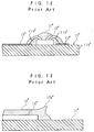
- the resin application path begins at one end of the array of the drive ICs 13'' and terminates at the opposite end thereof. Further, as shown in Fig. 13, a horn-like protrusion 17a'' may be formed at the terminal end of the resin application path. This is because the applied epoxy resin has the rather high viscosity and, at the terminal end of the application path, the projection nozzle of the dispenser is being shifted upward after the resin supply is stopped. Then, the protrusion 17a'' will be cured with the horn shape maintained.
- protrusion 17a'' of the protective coating 17'' may unfavorably damage a recording medium such as recording paper or deteriorate prints formed thereon through contact with the recording medium.
- a recording medium such as recording paper
- Such inconvenience will become more critical to the latest model of e.g. printing device, in which the feeding path of recording paper is disposed as close to the surface of the thermal printhead as possible for purposes of miniaturization for example.
- a head device which includes: an insulating substrate having a first longitudinal edge and a second longitudinal edge opposite to the first longitudinal edge; an operating element arranged on the substrate adjacent to the first longitudinal edge; an array of plural drive ICs arranged on the substrate along the second longitudinal edge for actuating the operating element; and a protective resin coating for enclosing the drive ICs.
- the protective coating includes a terminal protrusion which is made at the time of forming the protective coating by resin application.
- the head device is characterized by the terminal protrusion which projects toward the second edge of the substrate.
- the terminal protrusion projects downward toward the second edge of the substrate.
- the terminal protrusion is preferably positioned between a pair of adjacent drive ICs.
- the protective coating may be made of a heat-resisting resin.
- the heat-resisting resin may be a thermosetting resin such as epoxy resin for example, or a soft resin such as silicone resin for example.
- a typical head device to which the present invention is applicable is a thermal printhead, in which the operating element is a heating resistor.
- a head device which includes: an insulating substrate having a first longitudinal edge and a second longitudinal edge opposite to the first longitudinal edge; an operating element arranged on the substrate adjacent to the first longitudinal edge; an array of plural drive ICs mounted on the substrate and spaced from each other along the second longitudinal edge for actuating the operating element; and a protective resin coating for enclosing the drive ICs.
- the protective coating includes a terminal protrusion which is made at the time of forming the protective coating by resin application.
- the present invention is characterized by the terminal protrusion which is positioned between a pair of adjacent drive ICs.
- a method for forming a protective resin coating for a head device including an insulating substrate having a first longitudinal edge and a second longitudinal edge opposite to the first longitudinal edge, an operating element arranged on the substrate adjacent to the first longitudinal edge, and an array of plural drive ICs arranged on the substrate along the second longitudinal edge for actuating the operating element.
- the protective coating is used for enclosing the drive ICs.
- the method is characterized by the steps of applying a fluid resin from a projection nozzle along an elongated spiral path for enclosing the drive ICs; and stopping the resin application while the projection nozzle is being moved toward the second longitudinal edge of the substrate.
- the resin application is advantageously stopped while the projection nozzle is being moved downward toward the second longitudinal edge of the substrate.
- a method of forming a protective resin coating for a head device including an insulating substrate having a first longitudinal edge and a second longitudinal edge opposite to the first longitudinal edge, an operating element arranged on the substrate adjacent to the first longitudinal edge, and an array of plural drive ICs mounted on the substrate and spaced from each other along the second longitudinal edge for actuating the operating element.
- the protective coating is used for enclosing the drive ICs.
- the method is characterized by the steps of: applying a fluid resin from a projection nozzle along an elongated spiral path for enclosing the drive ICs; and stopping the resin application at a position between a pair of adjacent drive ICs.
- a thermal printhead 10 embodying the present invention has a basic arrangement typical of the so-called thick-film type thermal printhead.
- the thermal printhead 10 includes a heat sink plate 20 made of a metal having high thermal conductivity like aluminum.
- the printhead also includes an elongated rectangular head substrate 11 made of an insulating material such as alumina ceramic. The head substrate is mounted on the heat sink plate 20.
- the head substrate 11 includes a first longitudinal edge 11a and a second longitudinal edge 11b opposite to the first longitudinal edge 11a.
- the head substrate 11 has an upper surface provided with a heating resistor 12 extending along the first longitudinal edge 11a.
- the upper surface is also provided with an array of plural drive ICs 13 arranged along the second longitudinal edge 11b for actuating the heating resistor 12.
- the upper surface of the head substrate 11 is formed with a common electrode 14 adjacent to the heating resistor 12.
- the common electrode includes comb-like teeth 14a extending under the heating resistor 12.
- individual electrodes 15 arranged in an alternating manner relative to the teeth 14a of the common electrode 14.
- the individual electrodes 15 also extend under the heating resistor 12.
- the heating resistor 12 is divided into regions each of which is defined by adjacent teeth 14a of the common electrode 14 (see the shaded portion in Fig. 2). The above regions operate as heating dots 16.
- relevant heating dots 16 are actuated for heating.
- each individual electrode 15 extends toward the second longitudinal edge 11b of the head substrate 11.
- the individual electrode is connected to the output side of a corresponding drive IC 13 via a bonding wire 21a.
- the input side of the drive IC 13 is connected to a wiring pattern 22 (only schematically shown in Fig. 4) formed on the head substrate 11.
- the teeth 14a of the common electrode 14 are formed at intervals of 125 ⁇ m when a printing density of 200dpi is desired.
- the individual electrodes are formed at the same intervals.
- Minute wiring patters on the insulating substrate, including the common electrode 14 and the individual electrodes 15, may be formed by minutely etching a conductive film made of e.g. gold provided on the substrate.
- the drive ICs 13 on the head substrate 11, together with the bonding wires 21a, 21b connected to the drive ICs, are enclosed by a protective resin coating 17.
- the areas other than the above regions enclosed by the protective coating 17 may typically be covered by a protective layer (not shown) made of glass for example.
- the protective coating 17 is preferably made of a heat-resisting resin. In such an instance, use is made to a thermosetting resin such as epoxy resin and phenol resin, or to a soft resin such as silicone resin.
- the protective coating 17 is made in the following manner.
- a resin material such as epoxy resin for example
- the fluid resin material is supplied from a projection nozzle 18 (Fig. 5) as a resin dispenser while the projection nozzle is being shifted.
- the substrate 11 is brought into a heating furnace to cure the resin material.
- the present invention is characterized by the method of forming the protective coating 17 and by the form of the protective coating 17 made by the above method.
- Fig. 3 shows a first embodiment of the method for forming the protective coating 17.
- the moving path 19 of the projection nozzle 18 as seen from above is shown.
- the moving path 19 of the projection nozzle 18 has a starting point 191 located within the region A allotted for formation of the protective coating 17.
- the starting point is disposed in a longitudinally central portion of the region A and closer to the second longitudinal edge 11b of the head substrate 11.
- the moving path 19 winds twice inwardly in an elongated spiral manner.
- the moving path 19 terminates near the starting point 191, with its end portion (terminal end 192) projecting toward the second longitudinal edge 11b of the head substrate 11. It should be noted that both the starting point 191 and the terminal end 192 of the resin application are located between two adjacent drive ICs 13.
- the terminal end 192 of the resin application is formed by moving the projection nozzle 18 toward the second longitudinal edge 11b of the head substrate 11 while the resin supply is being stopped. In this operation, the projection nozzle 18 is preferably moved downward toward the second longitudinal edge 11b of the head substrate 11, as shown in Fig. 5, to complete the resin application.
- the epoxy resin is a material having predetermined viscosity.
- the terminal end 192 of the resin application is directed toward the second longitudinal edge 11b of the head substrate 11.
- the distance between the heating resistor 12 and the protrusion is rendered maximized.
- the above advantage is enjoyed more effectively by arranging the terminal end 192 of the resin application between two adjacent drive ICs 13. Specifically, as shown in Fig. 6, the surface of the protective coating 17 is lower at portions with no drive ICs 13 provided than at the other portions where the drive ICs 13 are provided. As a result, the protrusion 17a is prevented from projecting upward beyond the surface level of the protective coating 17 where the drive ICs 13 are enclosed.
- the terminal end 192 of the resin application is formed while the projection nozzle 18 is being shifted slightly downward. Consequently, as shown in Fig. 5, the whisker-like or horn-like protrusion 17a is directed downward relative to the horizontal direction. Thus, the protrusion is much less likely to contact recording paper.
- Fig. 7 shows the second embodiment of a method of forming the protective coating 17.
- another moving path 19 of the projection nozzle 18 as viewed above is shown.
- the same elements as those shown in Fig. 3 are indicated by the same reference numerals, whereas similar elements are indicated by the same numerals followed by a prime (').
- the starting point 191' of the moving path 19' of the projection nozzle 18 is arranged offset toward an end portion of the region A allotted for formation of the protective coating 17' from the longitudinally central portion of the region A.
- the moving path 19' winds twice inwardly in an elongated spiral manner, and terminates (at a terminal end 192') near the starting point 191'.
- both the starting point 191' and the terminal end 192' of the resin application are disposed between two adjacent drive ICs 13.
- the projection nozzle 18 is not shifted toward the second longitudinal edge 11b of the head substrate 11 nor downward.
- the surface of the protective coating 17' is lower at portions with no drive ICs 13 provided than at the portions with the drive ICs 13 provided.
- the terminal end 192' of the resin application is arranged between two adjacent drive ICs 13.
- the protrusion 17a' at the terminal end 192' is much less likely to project upwardly beyond the higher portions of the surface of the protective coating 17 with the drive ICs 13 provided.
- the present invention is not limited to these embodiments.
- the present invention is also applicable to the so-called thin-film type thermal printhead other than the thick-film type thermal printhead.
- the present invention is applicable to not only printheads but also other devices such as an image scanner head incorporating plural drive ICs which are mounted on an insulating substrate and enclosed by a protective coating.
Landscapes
- Electronic Switches (AREA)
- Particle Formation And Scattering Control In Inkjet Printers (AREA)
Abstract
Description
Claims (17)
- A head device comprising: an insulating substrate including a first longitudinal edge and a second longitudinal edge opposite to the first longitudinal edge; an operating element arranged on the substrate adjacent to the first longitudinal edge; an array of plural drive ICs arranged on the substrate along the second longitudinal edge for actuating the operating element; and a protective resin coating for enclosing the drive ICs, the protective coating including a terminal protrusion which is made at a time of forming the protective coating by resin application;
wherein the terminal protrusion projects toward the second edge of the substrate. - The head device according to claim 1, wherein the terminal protrusion projects downward toward the second edge of the substrate.
- The head device according to claim 1, wherein the drive ICs are spaced from each other, the terminal protrusion being positioned between a pair of adjacent drive ICs.
- The head device according to claim 1, wherein the protective coating is made of a heat-resisting resin.
- The head device according to claim 4, wherein the heat-resisting resin is a thermosetting resin.
- The head device according to claim 5, wherein the thermosetting resin is an epoxy resin.
- The head device according to claim 4, wherein the heat-resisting resin is a silicone resin.
- A thermal printhead as the head device according to claim 1, wherein the operating element is a heating resistor.
- A head device comprising: an insulating substrate including a first longitudinal edge and a second longitudinal edge opposite to the first longitudinal edge; an operating element arranged on the substrate adjacent to the first longitudinal edge; an array of plural drive ICs mounted on the substrate and spaced from each other along the second longitudinal edge for actuating the operating element; and a protective resin coating for enclosing the drive ICs, the protective coating including a terminal protrusion which is made at a time of forming the protective coating by resin application;
wherein the terminal protrusion is positioned between a pair of adjacent drive ICs. - The head device according to claim 9, wherein the protective coating is made of a heat-resisting resin.
- The head device according to claim 10, wherein the heat-resisting resin is a thermosetting resin.
- The head device according to claim 11, wherein the thermosetting resin is an epoxy resin.
- The head device according to claim 10, wherein the heat-resisting resin is a silicone resin.
- A thermal printhead as the head device according to claim 9, wherein the operating element is a heating resistor.
- A method of forming a protective resin coating for a head device which includes an insulating substrate having a first longitudinal edge and a second longitudinal edge opposite to the first longitudinal edge, an operating element arranged on the substrate adjacent to the first longitudinal edge, and an array of plural drive ICs arranged on the substrate along the second longitudinal edge for actuating the operating element, the protective coating enclosing the drive ICs, the method comprising:applying a fluid resin from a projection nozzle along an elongated spiral path for enclosing the drive ICs; and stopping the resin application while the projection nozzle is being moved toward the second longitudinal edge of the substrate.
- The method of forming a protective coating according to claim 15, wherein the resin application is stopped while the projection nozzle is being moved downward toward the second longitudinal edge of the substrate.
- A method of forming a protective resin coating for a head device which includes an insulating substrate having a first longitudinal edge and a second longitudinal edge opposite to the first longitudinal edge, an operating element arranged on the substrate adjacent to the first longitudinal edge, and an array of plural drive ICs mounted on the substrate and spaced from each other along the second longitudinal edge for actuating the operating element, the protective coating enclosing the drive ICs, the method comprising:applying a fluid resin from a projection nozzle along an elongated spiral path for enclosing the drive ICs; and stopping the resin application at a position between a pair of adjacent drive ICs.
Applications Claiming Priority (4)
| Application Number | Priority Date | Filing Date | Title |
|---|---|---|---|
| JP136336/96 | 1996-05-30 | ||
| JP13633696 | 1996-05-30 | ||
| JP13633696 | 1996-05-30 | ||
| PCT/JP1997/001864 WO1997045270A1 (en) | 1996-05-30 | 1997-05-29 | Head device provided with drive ics, to which protective coating is applied, and method of forming protective coating |
Publications (3)
| Publication Number | Publication Date |
|---|---|
| EP0842783A1 true EP0842783A1 (en) | 1998-05-20 |
| EP0842783A4 EP0842783A4 (en) | 1999-08-04 |
| EP0842783B1 EP0842783B1 (en) | 2002-07-31 |
Family
ID=15172841
Family Applications (1)
| Application Number | Title | Priority Date | Filing Date |
|---|---|---|---|
| EP97924288A Expired - Lifetime EP0842783B1 (en) | 1996-05-30 | 1997-05-29 | Head device provided with drive ics, to which protective coating is applied, and method of forming protective coating |
Country Status (9)
| Country | Link |
|---|---|
| US (1) | US6034706A (en) |
| EP (1) | EP0842783B1 (en) |
| JP (1) | JP3815623B2 (en) |
| KR (1) | KR100256391B1 (en) |
| CN (1) | CN1082453C (en) |
| CA (1) | CA2226957C (en) |
| DE (1) | DE69714381T2 (en) |
| TW (1) | TW334402B (en) |
| WO (1) | WO1997045270A1 (en) |
Families Citing this family (2)
| Publication number | Priority date | Publication date | Assignee | Title |
|---|---|---|---|---|
| WO2014080843A1 (en) * | 2012-11-20 | 2014-05-30 | 京セラ株式会社 | Thermal head and thermal printer provided with same |
| WO2015029913A1 (en) * | 2013-08-26 | 2015-03-05 | 京セラ株式会社 | Thermal head and thermal printer provided with same |
Family Cites Families (9)
| Publication number | Priority date | Publication date | Assignee | Title |
|---|---|---|---|---|
| CA1237019A (en) * | 1984-03-26 | 1988-05-24 | Toshio Matsuzaki | Thermal recording head and process for manufacturing wiring substrate therefor |
| KR920004866B1 (en) * | 1987-11-19 | 1992-06-19 | 마쓰시다 덴끼 산교오 가부시기 가이샤 | Thermal head |
| JPH0357656A (en) * | 1989-07-26 | 1991-03-13 | Nec Corp | Thermal head |
| US5157414A (en) * | 1989-09-08 | 1992-10-20 | Hitachi, Ltd. | Thick film type thermal head and thermal recording device |
| JPH04338556A (en) * | 1991-05-15 | 1992-11-25 | Rohm Co Ltd | Thermal printing head |
| JPH05270036A (en) * | 1992-03-27 | 1993-10-19 | Rohm Co Ltd | Thermal printing head |
| JP2909796B2 (en) * | 1993-12-28 | 1999-06-23 | ローム株式会社 | Thermal print head and method of manufacturing the same |
| KR0173431B1 (en) * | 1994-10-06 | 1999-04-01 | 사토 겐이치로 | Ic for driving printer and print head |
| JPH08132451A (en) * | 1994-11-07 | 1996-05-28 | Murata Mfg Co Ltd | Cutting of resin burr of electric part |
-
1997
- 1997-05-29 CN CN97190488A patent/CN1082453C/en not_active Expired - Lifetime
- 1997-05-29 KR KR1019980700215A patent/KR100256391B1/en not_active Expired - Fee Related
- 1997-05-29 EP EP97924288A patent/EP0842783B1/en not_active Expired - Lifetime
- 1997-05-29 CA CA002226957A patent/CA2226957C/en not_active Expired - Fee Related
- 1997-05-29 JP JP54204297A patent/JP3815623B2/en not_active Expired - Fee Related
- 1997-05-29 US US08/973,201 patent/US6034706A/en not_active Expired - Lifetime
- 1997-05-29 WO PCT/JP1997/001864 patent/WO1997045270A1/en not_active Ceased
- 1997-05-29 DE DE69714381T patent/DE69714381T2/en not_active Expired - Fee Related
- 1997-05-29 TW TW086107296A patent/TW334402B/en active
Also Published As
| Publication number | Publication date |
|---|---|
| EP0842783B1 (en) | 2002-07-31 |
| WO1997045270A1 (en) | 1997-12-04 |
| KR100256391B1 (en) | 2000-06-01 |
| JP3815623B2 (en) | 2006-08-30 |
| DE69714381T2 (en) | 2003-03-20 |
| KR19990028913A (en) | 1999-04-15 |
| CN1082453C (en) | 2002-04-10 |
| US6034706A (en) | 2000-03-07 |
| DE69714381D1 (en) | 2002-09-05 |
| CA2226957C (en) | 2003-02-04 |
| EP0842783A4 (en) | 1999-08-04 |
| CN1190370A (en) | 1998-08-12 |
| TW334402B (en) | 1998-06-21 |
| CA2226957A1 (en) | 1997-12-04 |
Similar Documents
| Publication | Publication Date | Title |
|---|---|---|
| US5485192A (en) | Thermal printhead | |
| US6331868B1 (en) | Thermal printhead and method of making the same | |
| US5680170A (en) | Thermal printhead | |
| CN112428696B (en) | Driver IC for thermal head, and thermal head | |
| EP0842783B1 (en) | Head device provided with drive ics, to which protective coating is applied, and method of forming protective coating | |
| US6326990B1 (en) | Thick film thermal head and method of manufacturing the same | |
| EP1077136B1 (en) | Thick-film thermal print head | |
| JP2001232838A (en) | Thermal printing head and manufacturing method | |
| US6304280B1 (en) | Thermal printhead and method of making the same | |
| EP0729840B1 (en) | Ic for driving printer and print head | |
| US6400388B1 (en) | Thick film thermal head and method of making the same | |
| JP5329887B2 (en) | Thermal head | |
| JP4163969B2 (en) | Thermal head, thermal printer using the same, and thermal head manufacturing method | |
| JPWO1997045270A1 (en) | Head device including driver IC with protective coating and method for forming the protective coating | |
| JP7557320B2 (en) | Thermal Printhead | |
| CN113386469B (en) | Thermal print head and method of manufacturing the same | |
| JP2023109505A (en) | Semiconductor element, packaging structure of the same, and thermal print head | |
| JPH02231153A (en) | thermal head | |
| JPH0592598A (en) | Thermal head | |
| JP2000135806A (en) | Thermal head | |
| JPH08183197A (en) | Manufacture of thermal head | |
| JPH0939282A (en) | Thermal head and manufacture thereof | |
| JPH03184877A (en) | Line type thermal print head | |
| JPS5945174A (en) | Thermal head | |
| JPH07171982A (en) | Thermal head |
Legal Events
| Date | Code | Title | Description |
|---|---|---|---|
| PUAI | Public reference made under article 153(3) epc to a published international application that has entered the european phase |
Free format text: ORIGINAL CODE: 0009012 |
|
| 17P | Request for examination filed |
Effective date: 19980130 |
|
| AK | Designated contracting states |
Kind code of ref document: A1 Designated state(s): DE FR GB NL |
|
| A4 | Supplementary search report drawn up and despatched |
Effective date: 19990621 |
|
| AK | Designated contracting states |
Kind code of ref document: A4 Designated state(s): DE FR GB NL |
|
| GRAG | Despatch of communication of intention to grant |
Free format text: ORIGINAL CODE: EPIDOS AGRA |
|
| GRAG | Despatch of communication of intention to grant |
Free format text: ORIGINAL CODE: EPIDOS AGRA |
|
| GRAH | Despatch of communication of intention to grant a patent |
Free format text: ORIGINAL CODE: EPIDOS IGRA |
|
| 17Q | First examination report despatched |
Effective date: 20011210 |
|
| GRAH | Despatch of communication of intention to grant a patent |
Free format text: ORIGINAL CODE: EPIDOS IGRA |
|
| GRAA | (expected) grant |
Free format text: ORIGINAL CODE: 0009210 |
|
| AK | Designated contracting states |
Kind code of ref document: B1 Designated state(s): DE FR GB NL |
|
| PG25 | Lapsed in a contracting state [announced via postgrant information from national office to epo] |
Ref country code: NL Free format text: LAPSE BECAUSE OF FAILURE TO SUBMIT A TRANSLATION OF THE DESCRIPTION OR TO PAY THE FEE WITHIN THE PRESCRIBED TIME-LIMIT Effective date: 20020731 |
|
| REG | Reference to a national code |
Ref country code: GB Ref legal event code: FG4D |
|
| REF | Corresponds to: |
Ref document number: 69714381 Country of ref document: DE Date of ref document: 20020905 |
|
| ET | Fr: translation filed | ||
| NLV1 | Nl: lapsed or annulled due to failure to fulfill the requirements of art. 29p and 29m of the patents act | ||
| PLBE | No opposition filed within time limit |
Free format text: ORIGINAL CODE: 0009261 |
|
| STAA | Information on the status of an ep patent application or granted ep patent |
Free format text: STATUS: NO OPPOSITION FILED WITHIN TIME LIMIT |
|
| 26N | No opposition filed |
Effective date: 20030506 |
|
| PGFP | Annual fee paid to national office [announced via postgrant information from national office to epo] |
Ref country code: GB Payment date: 20080604 Year of fee payment: 12 |
|
| PGFP | Annual fee paid to national office [announced via postgrant information from national office to epo] |
Ref country code: FR Payment date: 20090515 Year of fee payment: 13 Ref country code: DE Payment date: 20090527 Year of fee payment: 13 |
|
| GBPC | Gb: european patent ceased through non-payment of renewal fee |
Effective date: 20090529 |
|
| PG25 | Lapsed in a contracting state [announced via postgrant information from national office to epo] |
Ref country code: GB Free format text: LAPSE BECAUSE OF NON-PAYMENT OF DUE FEES Effective date: 20090529 |
|
| REG | Reference to a national code |
Ref country code: FR Ref legal event code: ST Effective date: 20110131 |
|
| PG25 | Lapsed in a contracting state [announced via postgrant information from national office to epo] |
Ref country code: DE Free format text: LAPSE BECAUSE OF NON-PAYMENT OF DUE FEES Effective date: 20101201 |
|
| PG25 | Lapsed in a contracting state [announced via postgrant information from national office to epo] |
Ref country code: FR Free format text: LAPSE BECAUSE OF NON-PAYMENT OF DUE FEES Effective date: 20100531 |