BACKGROUND OF THE INVENTION
1. FIELD OF THE INVENTION
The present invention relates to a motherboard for a personal
computer that automatically configures itself for the speed,
multiplier and voltage required for the type of microprocessor,
(CPU), installed in the motherboard.
2. DESCRIPTION OF THE PRIOR ART
Today's personal computers are evolving at an ever increasing
speed. Since the introduction of Intel's 386DX there have been
several types of CPUs manufactured for each series. For each type
of CPU three parameters must be selected, and these include the
frequency, (ranging from 33MHz-75MHz), multiplier of the CPU
frequency, (ranging from 1.5-3), and operating voltage, (including
5 volts, 3.3 volts, 2.5 volts, etc.). The frequency, voltage and
multiplier for each type of microprocessor are normally selected by
changing jumpers or dip-switches located on the motherboard.
Several other methods for reconfiguration different computer
options have been employed by prior art devices and the following
documents illustrate some of these. U.S. Patent No. 4,967,346,
(Freidin) discloses a universal microprocessor interface for
accepting different processors on the same motherboard. U.S.
Patent No. 5,371,892, (Petersen et al.) discloses a method for
upgrading a personal computer by utilizing the set-up (i.e., power
up) initialization of the computer to change any settings
identifying upgrades. European Patent Document No. 0,510,241
discloses a computer system for changing the particular processor,
(i486), having differing clock speeds without having to alter any
jumper or dip-switch settings. British Patent No. 2,271,446
discloses a kit for a user to build a computer, having simplified
upgradable characteristics.
None of the above inventions and patents, taken either singly
or in combination, is seen to describe the instant invention as
claimed.
SUMMARY OF THE INVENTION
The present invention is a logic circuit and a special module
of BIOS for a computer motherboard that automatically reconfigures
the motherboard to accept different microprocessors, (CPUs). Each
series of CPUs, (486, Pentium, Pentium Pro, etc.), includes
different types having different parameters including:
manufacturers, (Intel, AMD, Cyrix, etc.); basic frequencies,
(50MHz, 60MHz, 66MHz, 75MHz, etc.) multipliers, (1.5X, 2.0X, 2.5X,
3.0X, etc.); and operating voltages, (3.3V, 2.8V, etc.). As
discussed above, these different parameters must be set on a
conventional motherboard by opening and closing jumpers and/or dip-switches.
Many times more than five jumpers or dip-switches must
be changed when the CPU is upgraded to a different type. These
jumpers and dip-switches are often in hard to reach areas of the
motherboard, and usually require removing the motherboard from the
computer case. The present invention avoids the need for changing
these jumpers or switches by using the Basic Input/Output System,
(BIOS), to instruct a logic circuit to set the proper voltage,
frequency and multiplier for the specific CPU installed in the
motherboard. When a user wishes to upgrade their computer, they
need only remove the old CPU, insert the new CPU and turn on the
computer. In many computers the CPU can be changed by simply
opening the computer's case, and does not require removing the
motherboard from the case. When the computer "powers up" the
operating system senses whether a "hot key", (this can be
preprogrammed to be any of the keys on the keyboard), is being or
has been pressed. When the hot key has been pressed, the computer
enters BIOS setup and the operator can then change the CPU
parameters, (voltage, frequency and multiplier), as displayed on
the screen. If the hot key is not pressed, the computer simply
uses the parameters as previously defined. As with conventional
personal computers, the BIOS can be entered from resets other than
power-up and the CPU configuration can be changed without turning
the computer off.
Accordingly, it is a principal object of the invention to
allow an operator to up-grade the CPU of their personal computer
without having to remove the motherboard from the computer or reset
jumpers and/or dip-switches.
It is another object of the invention to allow changing the
configuration of the computer using BIOS only.
It is an object of the invention to provide improved elements
and arrangements thereof in an apparatus for the purposes described
which is inexpensive, dependable and fully effective in
accomplishing its intended purposes.
These and other objects of the present invention will become
readily apparent upon further review of the following specification
and drawings.
BRIEF DESCRIPTION OF THE DRAWINGS
Fig. 1 is a circuit diagram of the control logic used to set
the CPU frequency, multiplier and voltage in accordance with the
present invention.
Fig. 2 is a circuit diagram of the CPU, voltage generator and
clock chip as controlled by the present invention.
Fig. 3 is a flow chart of the BIOS operation used to set the
CPU frequency, multiplier and voltage in accordance with the
present invention.
Fig. 4 is a circuit diagram of the CPU, voltage generator and
clock chip as controlled by jumpers in prior art motherboards.
Similar reference characters denote corresponding features
consistently throughout the attached drawings.
DETAILED DESCRIPTION OF THE PREFERRED EMBODIMENT
The present invention is drawn to configuring a computer
motherboard to operate with a specific microprocessor. In
conventional computer motherboards, the operating voltage,
frequency and multiplier are selected by physically changing
jumpers or dip-switches on the motherboard. Figure 4 shows one
type of prior art circuit used to accomplish this. A
microprocessor 400 has inputs for an
operating voltage 402,
multiplier selectors 406, (BF-1 and BF-2), and a
CPU clock 408.
The operating voltage is provided by a
CPU voltage generator 401
that determines the proper voltage by reading three
inputs 404,
(VCC2A, VCC2B, and VCC3). The
CPU clock input 408 operates at a
frequency determined by reading three
inputs 407, (SEL1, SEL2 and
SEL3). The
multiplier selectors 406,
voltage determining inputs
404 and
frequency determining inputs 407 are tied to ground using
jumpers, (or closing dip-switches), to provide logic low levels.
For inputs that require a logic high level, the jumpers are
removed, (or the dip-switches are opened), and pull-
up resisters
405 provide V
cc potential. High-low combinations of these inputs
select the various functions as listed in Table 1 below.
| | CPU Frequency Selection |
| | FO1 | FO2 | FO3 | FO4 | FO5 | FO6 | FO7 |
| SEL1 | 0 | 1 | 0 | 1 | 0 | 1 | 0 |
| SEL2 | 0 | 0 | 1 | 1 | 0 | 0 | 1 |
| SEL3 | 0 | 0 | 0 | 0 | 1 | 1 | 1 |
| | CPU Voltage Selection |
| | V1 | V2 | V3 | V4 | V5 | V6 | V7 |
| VCC2A | 0 | 1 | 0 | 1 | 0 | 1 | 0 |
| VCC2B | 0 | 0 | 1 | 1 | 0 | 0 | 1 |
| VCC3 | 0 | 0 | 0 | 0 | 1 | 1 | 1 |
| | CPU Multiplier Selection |
| | X1.5 | | X2 | | X2.5 | | X3 |
| BF1 | 1 | | 0 | | 0 | | 1 |
| BF2 | 1 | | 1 | | 0 | | 0 |
The above table illustrates the method different frequencies,
voltages and multipliers are selected for specific microprocessors.
It should be noted that the different frequencies, (FO1-FO7), range
from 33MHz to 75MHz and therefore the frequency settings would
follow a format similar to FO1 = 33MHz, FO7 =75MHz, with the
intermediate steps, (FO2-FO6), being increments therebetween. The
different voltages are arranged in a like manner wherein V1 may
equal 2.8 volts, V2 may equal 3.3 volts, etc. These values for the
frequencies, voltages and multipliers, (listed in Table 1), are
given only as examples, and the actual values would be displayed
and selected using the BIOS of the particular computer in use.
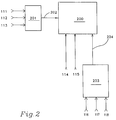
While the circuit shown in figure 4 is prior art, the present
invention uses the same setup as the microprocessor, CPU clock and
CPU voltage generator. The difference between the prior art
circuit and the circuit of the present invention can be seen by
viewing figure 2. This circuit includes a microprocessor 200, a
CPU clock 203 and a CPU voltage generator 201, however, it should
be noted that the jumpers, (or dip-switches) and the pull-up
resisters 405 have been eliminated as unnecessary for the circuit
of the present invention. SEL1, SEL2 and SEL3 are listed in figure
2 as 116-118 respectively, BF1 and BF2 are listed as 115 and 114
respectively, and VCC2A, VCC2B and VCC3 are listed as 113-111
respectively. As in the prior art the CPU voltage generator
supplies the CPU with operating voltage at line 202, while the CPU
clock supplies the clock frequency at line 204.
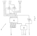
The various selection inputs to control the circuit in figure
2 are generated using the logic circuit 100 shown in figure 1.
Data latches 101 are connected to eleven of the computer data lines
106 that provide the programming information when the CPU 200 is
prompted by the BIOS program. A decoder 102 triggers the data
latches 101 when the correct address is provided via address line
107. Lines 108 and 109 are WR and RD respectively and are also
used by the CPU 200 and BIOS to prompt the decoder 102 to download
the data lines' information via the data latches 101 for
reconfiguration. The decoder 102 also triggers solid state relay
105 by providing a logic low level to the control port of the solid
state relay 105. When the solid state relay 105 is triggered it
provides a "data in" signal at 110 to the CPU which signals the CPU
that the new parameters have been provided at lines 111-118, and
assists in testing the reset status. Two additional solid state
relays, 103 and 104 are provided on the 114 and 115 lines, (BF2 and
BF1 respectively), and these relays operate in a similar manner to
solid state relay 105, and are triggered by two of the eleven data
lines, (after being latched by data latches 101). Solid state
relays 103-105 are necessary because several other devices also
drive the data in, BF1 and BF2 lines, and these devices insure that
two devices do not attempt to drive the same line at the same time.
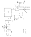
Figure 3 is a flow chart explaining the operation of the BIOS
software used to configure the motherboard via the control logic
explained above. Any type of reset, (system power on, system reset
and CPU reset), will initialize the BIOS at "Start" block 300. The
system then proceeds to the Initialization block 301 where certain
system components are reset, (depending on the type of reset as is
well known in the art), such as clearing RAM, spinning up any hard
drives, etc. From the Initialization block 301 the system proceeds
to block 302, where it is determined if the reset was caused by
powering up the computer. At this point we will consider that the
reset was caused by powering up the computer, (as would be
necessary when replacing the CPU), and following the "Yes" line the
system proceeds to block 303. In block 303 it is determined if the
"Hot Key" has been pressed by the computer operator. After the CPU
has been replaced with a different type of CPU, the operator must
turn on the computer and also press the Hot Key to enter the BIOS
configuration setup. Assuming this is the case, the system
proceeds from block 303 to block 304. In block 304 the BIOS setup
subroutine is entered and the BIOS screen is displayed on the PC's
monitor, (as is well known in the art). The difference between the
BIOS screen displayed by prior art devices and the present
invention is that the BIOS screen of the present invention has
blocks for entering the CPU frequency, multiplier and voltage as
discussed in detail above. After the operator has entered, in
block 305, the parameters for their specific CPU, (usually supplied
by the CPU manufacturer in the CPU's package), the CPU saves these
parameters, block 306, by using the CMOS RAM of the motherboard and
the data latches 101 as explained above. Once the parameters have
been saved, the system resets, a "Speed Easy" reset as named by the
inventor, at block 307 and the system returns to block 300.
If the power up reset had not been followed by the operator
pressing the Hot Key, the system would proceed from block 303 to
block 308. In block 308 the previously defined parameters, (stored
in the CMOS RAM), are used to operate the CPU. The system then
proceeds to block 309 which gives a standard reset and returns the
system to block 300.
If the reset is not of a power up type, (system reset, CPU
reset, or Speed Easy reset), the system proceeds from block 302 to
block 310. At block 310 the operator is given the option to enter
BIOS setup as is standard in conventional computer systems,
(usually by pressing the DEL key during boot-up). If the operator
enters BIOS setup, the system proceeds from block 310 to block 311,
and the BIOS setup continues through blocks 312-314 as explained
above for blocks 305-307. It should be noted that whenever BIOS
setup is entered, blocks 304 and 311, not only can the parameters
for the CPU be changed, but all of the standard computer
parameters, (RAM, I/O ports, etc.), can be changed as is well known
in the PC art. If BIOS setup is not entered, the system proceeds
from block 310 to block 315 where the processor is reset. After
the processor is reset, (not to be confused with CPU reset), the
system proceeds to block 316, the boot up sequence is completed,
and the disc operating system, DOS, is entered. From the above
information, it can be seen that a power on reset without
intervention on the part of the operator, will proceed as follows:
block 300 to block 301 to block 302 to block 303 to block 308 to
block 309 to block 300 to block 301 to block 302 to block 310 to
block 315 to block 316. A non-power up reset, (pressing the system
reset button on the computer case, or pressing control, ALT and DEL
keys simultaneously for a CPU reset), without further intervention
on the part of the operator, will proceed as follows: block 300 to
block 301 to block 302 to block 310 to block 315 to block 316.
It should be noted that the above invention is not limited to
a complete motherboard, but may be retro-fitted on an existing
motherboard by use of a module containing the circuitry of figures
1 and 2. In either case the systems BIOS program must be replaced
with the BIOS program of the present invention.
It is to be understood that the present invention is not
limited to the sole embodiment described above, but encompasses any
and all embodiments within the scope of the following claims.