EP0840323B1 - Static semiconductor memory device with precharging circuits having similar configuration of memory cells - Google Patents
Static semiconductor memory device with precharging circuits having similar configuration of memory cells Download PDFInfo
- Publication number
- EP0840323B1 EP0840323B1 EP97118438A EP97118438A EP0840323B1 EP 0840323 B1 EP0840323 B1 EP 0840323B1 EP 97118438 A EP97118438 A EP 97118438A EP 97118438 A EP97118438 A EP 97118438A EP 0840323 B1 EP0840323 B1 EP 0840323B1
- Authority
- EP
- European Patent Office
- Prior art keywords
- precharging
- node
- power supply
- memory cell
- memory cells
- Prior art date
- Legal status (The legal status is an assumption and is not a legal conclusion. Google has not performed a legal analysis and makes no representation as to the accuracy of the status listed.)
- Expired - Lifetime
Links
Images


Classifications
-
- G—PHYSICS
- G11—INFORMATION STORAGE
- G11C—STATIC STORES
- G11C11/00—Digital stores characterised by the use of particular electric or magnetic storage elements; Storage elements therefor
- G11C11/21—Digital stores characterised by the use of particular electric or magnetic storage elements; Storage elements therefor using electric elements
- G11C11/34—Digital stores characterised by the use of particular electric or magnetic storage elements; Storage elements therefor using electric elements using semiconductor devices
- G11C11/40—Digital stores characterised by the use of particular electric or magnetic storage elements; Storage elements therefor using electric elements using semiconductor devices using transistors
- G11C11/41—Digital stores characterised by the use of particular electric or magnetic storage elements; Storage elements therefor using electric elements using semiconductor devices using transistors forming static cells with positive feedback, i.e. cells not needing refreshing or charge regeneration, e.g. bistable multivibrator or Schmitt trigger
- G11C11/413—Auxiliary circuits, e.g. for addressing, decoding, driving, writing, sensing, timing or power reduction
- G11C11/417—Auxiliary circuits, e.g. for addressing, decoding, driving, writing, sensing, timing or power reduction for memory cells of the field-effect type
- G11C11/419—Read-write [R-W] circuits
-
- G—PHYSICS
- G11—INFORMATION STORAGE
- G11C—STATIC STORES
- G11C7/00—Arrangements for writing information into, or reading information out from, a digital store
- G11C7/12—Bit line control circuits, e.g. drivers, boosters, pull-up circuits, pull-down circuits, precharging circuits, equalising circuits, for bit lines
Definitions
- the present invention relates to a semiconductor device and, more particularly, to a static random access memory (SRAM) device.
- SRAM static random access memory
- a prior art SRAM device includes a plurality of word lines, a plurality of bit line pairs, at least one precharging line, a plurality of static memory cells connected to one of the word lines and one of the bit line pairs, and a plurality of precharging circuits connected to the precharging line and one of the bit line pairs, thus charging the one of the bit line pairs.
- the density of elements in the memory cell area of the static memory cells is much higher than that in the precharging circuits. This degrades the operation characteristics of the device.
- inactive dummy memory cells having the same configuration as the memory cells are inserted between the memory cell area and the precharging circuits. This will be explained later in detail.
- this object is achieved by a memory device as defined by claim 1.
- the precharging circuits also serve as inactive dummy memory cells, such inactive dummy memory cells can be omitted.
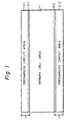
- Fig. 1 which is a layout diagram illustrating a first prior art SRAM device
- reference numeral 1 designates a memory cell area
- 2-1 and 2-2 designate dummy memory cell areas
- 3-1 and 3-2 designate precharging circuit areas.
- the memory cell area 1 includes memory cells C 11 to C n1 each connected to one of word lines WL 1 to WL n and complementary bit lines BL 1 and BL 1 .
- the dummy memory cell area 2-1 (2-2) includes one dummy memory cell DC 11 (DC 21 ) connected to one dummy word line DWL 1 (DWL 2 ) and the bit lines BL 1 and BL 1 .
- the precharging circuit area 3-1 (3-2) includes one precharging circuit PR 11 (PR 21 ) connected to the bit lines BL 1 and BL 1 .
- the precharging circuit PR 1 (PR 2 ) is controlled by a precharging clock signal ⁇ PR . That is the bit lines BL 1 and BL 1 are precharged at V cc after each read or write operation, thus increasing the read or write operation speed.
- the memory cell such as C 11 is provided at each intersection between the word line WL 1 and the bit lines BL 1 and BL 1 .
- the memory cell C 11 is constructed by a flip-flop formed by two cross-coupled inverters and two transfer transistors Q t1 and Q t2 between nodes N 1 and N 2 of the flip-flop and the bit lines BL 1 and BL 1 .
- the transfer transistors Q t1 and Q t2 are controlled by the voltage at the word line WL 1 .
- Each of the inverters is formed by a load resistor R 1 (R 2 ) and a drive transistor Q d1 (Q d2 ) between a power supply line denoted by V cc and a ground line denoted by GND.
- the node N 1 is connected to a gate of the drive transistor Q d2 , so that the drive transistor Q d2 is driven by the voltage at the node N 1 .
- the node N 2 is connected to a gate of the drive transistor Q d1 , so that the drive transistor Q d1 is driven by the voltage at the node N 2 .
- the dummy memory cell such as DC 21 has the same configuration as the memory cell C 11 of the memory cell area 1. However, note that the dummy word line DWL 2 is grounded, so that the dummy memory cell DC 2 is completely inactive.
- the precharging circuit such as PR 21 is constructed by a transistor Q PR1 connected between the power supply line V cc and the bit line BL 1 and a transistor Q PR2 connected between the power supply line V cc and the bit line BL 1 .
- the density of elements in the memory cell area 1 is much higher than that in the precharging circuit areas 3-1 and 3-2. This degrades the operation characteristics of the device.
- the inactive dummy memory cells such as DC 11 and DC 21 having the same configuration as the memory cells are inserted between the memory cell area 1 and the precharging circuit areas 3-1 and 3-2.
- the memory cell such as C 11 and the dummy memory cell such as DC 21 are actually symmerical with respect to a center location thereof, so that the memory cells and the dummy memory cells are balanced. As a result, data retention characteristics and soft error resistance characteristics can be improved.
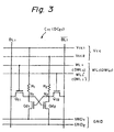
- the circuit diagram of the memory cell C 11 (the dummy memory cell DC 21 ) is actually as illustrated in Fig.
- the power supply line V cc is replaced by two power supply lines V cc1 and V cc2 whose voltages are the same as each other;
- the word line WL 1 (the dummy word line DWL 1 ) is replaced by two word lines WL 1 and WL 1 '(DWL 1 and DWL 1 ') whose voltages are the same as each other;
- the ground line GND is replaced by two ground lines GND 1 and GND 2 whose voltages are the same as each other.
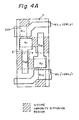
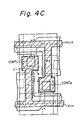
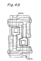
- FIG. 4A An example of the memory cell C 11 (the dummy memory cell DC 21 ) of Fig. 2 is illustrated in Figs. 4A, 4B, 4C and 4D.
- a P-type monocrystalline silicon substrate (not shown) is thermally oxidized to form a field silicon oxide layer F by using a local oxidation of silicon (LOCOS) process.
- LOC local oxidation of silicon
- a gate silicon oxide layer GOX is formed by thermally oxidizing the substrate.
- gate electrodes of the transistors Q t1 , Q t2 , Q d1 , and Q d2 are formed.
- the gate electrodes of the transistors Q t1 and Q t2 also serve as the word lines WL 1 and WL 1 ' (the dummy word lines DWL 1 and DWL 1 '), respectively.
- N-type impurity ions are implanted into the substrate using the gate electrodes as a mask to form N-type impurity diffusion regions as indicated by shaded portions.
- the field silicon oxide layer F, the gate electrodes and the N-type impurity diffusion regions are symmetrical with respect to the center location thereof as indicated by Z.
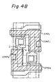
- a metal (tungsten or the like) layer is formed on an insulating layer (not shown), and is patterned to form the ground lines GND 1 and GND 2 .
- the ground lines GND 1 and GND 2 are connected via contact holes CONT 1 and CONT 2 to sources of the drive transistors Q d1 and Q d2 , respectively.
- ground lines GND 1 , and GND 2 are symmetrical with respect to the center location thereof as indicated by Z.
- a metal (tungsten or the like) layer is formed on an insulating layer (not shown), and a patterned to form the power supply lines V cc1 , and V cc2 .
- the ground lines V cc1 and V cc2 are connected via contact holes CONT 3 and CONT 4 to the nodes N 1 and N 2 , respectively.
- the load resistors R 1 (R 2 ) are formed between the power supply lines V cc1 (V cc2 ) and the contact holes CONT 3 (CONT 4 ).
- the power supply lines V cc1 and V cc2 are symmetrical with respect to the center location thereof as indicated by Z.
- an aluminum layer (not shown) is formed on an insulating layer (not shown) and is patterned to form the bit lines BL 1 and BL 1 (not shown).
- the bit lines BL 1 and BL 1 are connected via contact holes CONT 5 and CONT 6 to the drains of the transfer transistors Q t1 and Q t2 , respectively.
- bit lines BL 1 and BL 1 are symmetrical with respect to the center location thereof as indicated by Z.
- Fig. 5 is a layout diagram illustrating a second prior art SRAM device
- Fig. 6 is a circuit diagram of one column of the device of Fig. 5.
- Figs. 5 and 6 in order to homogenize precharging currents in the device of Fig. 1, three precharging circuit areas 3-1, 3-2 and 3-3 are provided.
- the memory cell area 1 of Fig. 1 is divided into two memory cell areas 1-1 and 1-2. Therefore, dummy memory cell areas 2-1, 2-2, 2-3 and 2-4 are required between the memory cell areas 1-1 and 1-2 and the precharging circuit areas 3-1, 3-2, 3-3 and 3-4.
- the length L 1 of the precharging circuit area 3-1 (3-3) and the dummy memory cell area 2-1 (2-4) is large, for example, about twenty times the longitudinal length of one memory cell, and also, the length L 2 of the precharging circuit 3-2 and the dummy memory areas 2-2 and 2-3 is larger than the length L 1 . Therefore, since 2L 1 + L 2 >2L 1 (first prior art), the integration is further reduced.
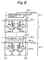
- Fig. 7 is a layout diagram illustrating a first embodiment of the SRAM device according to the present invention
- the dummy memory cell areas 2-1 and 2-2 of Fig. 1 are deleted, and the precharging circuit areas 3-1 and 3-2 are modified to precharging circuit areas 3-1' and 3-2', respectively.
- the precharging circuit area 3-1' (3-2') includes one precharging circuit PR 11 ' (PR 21 ') connected to the bit lines BL 1 and BL 1 .
- the precharging circuit PR 1 ' (PR 2 ') is connected to a precharging line PRL 1 (PRL 2 ) which controlled by a precharging clock signal ⁇ PR .
- the precharging line PRL 1 (PRL 2 ) corresponds to the word line such as WL 1 .
- the precharging circuit such as PR 21 ' has a similar configuration to the memory cell C 11 . That is, the precharging circit such as PR 21 ', is provided at each intersection between the word line WL 1 and the bit lines BL 1 and BL 1 .
- the precharging circuit PR 2 ' is constructed by a cross-coupled balancer and two transfer transistors Q t1 ' and Q t2 ' between nodes N 1 ' and N 2 ' of the balancer and the bit lines BL 1 and BL 1 .
- the transfer transistors Q t1 ' and Q t2 ' are controlled by the voltage at the precharging line PRL 2 .
- Each element of the balancer is formed by a load resistor R 1 ' (R 2 ') and a drive transistor Q d1 ' (Q d2 ') connected to the power supply line V cc .
- the node N 1 ' is connected to a gate of the drive transistor Q d2 ', so that the drive transistor Q d2 ' is driven by the voltage at the node N 1 '.
- the node N 2 ' is connected to a gate of the drive transistor Q d1 ', so that the drive transistor Q d1 ' is driven by the voltage at the node N 2 '.
- the precharging circuit PR 11 ' (PR 21 ') has a similar configuration to the memory cell such as C 11 , the precharging circuit PR 11 ', (PR 21 ') can also serve as the dummy memory cell DC 11 (DC 21 ) of Fig. 2.
- the precharging circuit such as, PR 21 ' is actually symmetrical with respect to a center location thereof, so that the precharging circuit PR 21 ' is balanced.
- the circuit diagram of the precharging circuit PR 21 ' is actually as illustrated in Fig. 9, where the power supply line V cc is replaced by two power supply lines V cc1 and V cc2 whose voltages are the same as each other; the precharging line PRL 2 is replaced by two word lines PRL 2 and PRL 2 ' whose voltages are the same as each other; and the ground line GND is replaced by two ground lines GND 1 and GND 2 whose voltages are the same as each other.
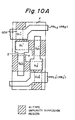
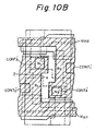
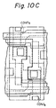
- FIG. 10A, 10B, 10C and 10D An example of the precharging circuit PR 2 ' is illustrated in Figs. 10A, 10B, 10C and 10D.
- a P-type monocrystalline silicon substrate (not shown) is thermally oxidized to form a field silicon oxide layer F by using a LOCOS process. Thereafter, a gate silicon oxide layer GOX is formed by thermally oxidizing the substrate. Then, gate electrodes of the transistors Q t1 ', Q t2 ', Q d1 ' and Q d2 ' are formed. In this case, the gate electrodes of the transistors Q t1 ' and Q t2 ' also serve as the precharging lines PRL 2 and PRL 2 ', respectively. Then, N-type impurity ions are implanted into the substrate using the gate electrodes as a mask to form N-type impurity diffusion regions as indicated by shaded portions.
- the field silicon oxide layer F, the gate electrodes and the N-type impurity diffusion regions are also symmetrical with respect to the center location thereof as indicated by Z.
- a metal (tungsten or the like) layer is formed on an insulating layer (not shown), and is patterned to form the power supply lines V cc1 , and V cc2 .
- the power supply line V cc1 is connected via contact holes CONT 2 ' and CONT 3 ' to a source of the drive transistor Q d2 ' and the node N 1 '.
- the power supply line V cc2 is connected via contact holes CONT 1 ' and CONT 4 ' to a source of the drive transistor Q d1 ' and the node N 2 '.
- the load resistors R 1 (R 2 ) are formed between the power supply lines V cc1 (V cc2 ) and the contact holes CONT 3 ' (CONT 4 ').
- the power supply lines V cc1 and V cc2 are also symmetrical with respect to the center location thereof as indicated by Z.
- an aluminum layer (not shown) is formed on an insulating layer (not shown) and is patterned to form the bit lines BL 1 and BL 1 (not shown).
- the bit lines BL 1 and BL 1 are connected via contact holes CONT 5 and CONT 6 to the drains of the transfer transistors Q t1 ' and Q t2 ', respectively.
- bit lines BL 1 and BL 1 are also symmetrical with respect the center location thereof as indicated by Z.
- the precharging circuit PR 21 ' as illustrated in Figs. 10A, 10B and 10C can be manufactured simultaneously with the memory cell C 11 as illustrated in Figs. 4A, 4B, 4C and 4D.
- ions are implanted into the power supply lines V cc1 and V cc2 only within the precharging circuit areas 3-1' and 3-2', to reduce the resistance values of the load resistors R 1 ' and R 2 ', thus increasing the current supply ability of the precharging circuits to the bit lines such as BL 1 and BL 1 .
- the amount of ions implanted into channel portions of the transistors Q t1 ', Q t2 ', Q d1 ' and Q d2 ' of the precharging circuits is reduced as compared with the amount of ions implanted into channel portions of the transistors Q t1 , Q t2 , Q d1 and Q d2 of the memory cells.
- the threshold voltages of the transistors Q t1' , Q t2' , Q d1' and Q d2' of the precharging circuits are reduced as compared with those of the transistors Q t1 , Q t2 , Q d1 and Q d2 of the memory cells. This also increases the current supply ability of the precharging circuits to the bit lines such as BL 1 and BL 1 .
- the integration can be enhanced.
- the cross-coupled balancer circuit configuration of the precharging circuit such as PR 21 enhances the charging speed of the bit lines BL 1 and BL 1 .
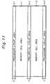
- Fig. 11 is a layout diagram illustrating a second embodiment of the SRAM device according to the present invention
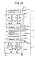
- Fig. 12 is a circuit diagram of one column of the device of Fig. 11.
- Figs. 11 and 12 in order to homogenize precharging currents in the device of Fig. 7, three precharging circuit areas 3-1', 3-2' and 3-3' are provided.
- the memroy cell area 1 of Fig. 7 is divided into two memory cell areas 1-1 and 1-2.
- the dummy memory cell areas 2-1, 2-2, 2-3 and 2-4 of Figs. 5 and 6 are deleted. Since the precharging circuit areas 3-1', 3-2' and 3-3' serve as dummy memory cell areas.
- the length L 1 ' of the precharging circuit area 3-1' (3-2', 3-3') is small, for example, about ten times as the longitudinal length of one memory cell. Therefore, since 3L 1 ' ⁇ 2L 1 + L 2 (second prior art), the integration is enhanced.
- precharging circuits also serve as dummy memory cells, the dummy memory cells can be omitted, thus enhancing the integration.
Description
- The present invention relates to a semiconductor device and, more particularly, to a static random access memory (SRAM) device.
- A prior art SRAM device includes a plurality of word lines, a plurality of bit line pairs, at least one precharging line, a plurality of static memory cells connected to one of the word lines and one of the bit line pairs, and a plurality of precharging circuits connected to the precharging line and one of the bit line pairs, thus charging the one of the bit line pairs. In this device, the density of elements in the memory cell area of the static memory cells is much higher than that in the precharging circuits. This degrades the operation characteristics of the device. For avoiding the degration of the operation characteristics, inactive dummy memory cells having the same configuration as the memory cells are inserted between the memory cell area and the precharging circuits. This will be explained later in detail.
- In the above-described prior art SRAM device, however, since the inactive dummy memory cells are necessary, the integration of the device is reduced.
- From US-A-4,972,377 a low-voltage low-power static RAM is known. This memory device has precharging circuits having a configuration similar to that of the memory cells.
- It is an object of the present invention to enhance the integration of an SRAM device.
- According to the present invention, this object is achieved by a memory device as defined by
claim 1. - Since the precharging circuits also serve as inactive dummy memory cells, such inactive dummy memory cells can be omitted.
- The present invention will be more clearly understood from the description as set forth below, in comparison with the prior art, with reference to the accompanying drawings, wherein:
- Fig. 1 is a layout diagram illustrating a first prior art SRAM device;
- Fig. 2 is a circuit diagram of one column of the device of Fig. 1;
- Fig. 3 is an equivalent circuit diagram of the memory cell (the dummy memory cell) of Fig. 2;
- Figs. 4A, 4B, 4C and 4D are plan views of the memory cell (the dummy memory cell) of Fig. 2;
- Fig. 5 is a layout diagram illustrating a second prior art SRAM device;
- Fig. 6 is 8 circuit diagram of one column of the device of Fig. 5;
- Fig. 7 is a layout diagram illustrating a first embodiment of the SRAM device according to the present invention;
- Fig. 8 is a circuit diagram of one column of the device of Fig. 7;
- Fig. 9 is an equivalent circuit diagram of the precharging circuit of Fig. 8;
- Figs. 10A, 10B and 10C are plan views of the precharging circuit of Fig. 8;
- Fig. 11 is a layout diagram illustrating a second embodiment of the SRAM device according to the present invention; and
- Fig. 12 is a circuit diagram of one column of the device of Fig. 11.
-
- Before the description of the preferred embodiments, prior art SRAM devices will be explained with reference to Figs. 1, 2, 3, 4A, 4B, 4C, 4D, 5 and 6.
- In Fig. 1, which is a layout diagram illustrating a first prior art SRAM device,
reference numeral 1 designates a memory cell area, 2-1 and 2-2 designate dummy memory cell areas, and 3-1 and 3-2 designate precharging circuit areas. - In Fig. 2, which is a circuit diagram of one column of the device of Fig. 1, the
memory cell area 1 includes memory cells C11 to Cn1 each connected to one of word lines WL1 to WLn and complementary bit lines BL1 andBL1 . Also, the dummy memory cell area 2-1 (2-2) includes one dummy memory cell DC11 (DC21) connected to one dummy word line DWL1 (DWL2) and the bit lines BL1 andBL1 . Further, the precharging circuit area 3-1 (3-2) includes one precharging circuit PR11 (PR21) connected to the bit lines BL1 andBL1 . The precharging circuit PR1 (PR2) is controlled by a precharging clock signal PR. That is the bit lines BL1 andBL1 are precharged at Vcc after each read or write operation, thus increasing the read or write operation speed. - The memory cell such as C11 is provided at each intersection between the word line WL1 and the bit lines BL1 and
BL1 . The memory cell C11 is constructed by a flip-flop formed by two cross-coupled inverters and two transfer transistors Qt1 and Qt2 between nodes N1 and N2 of the flip-flop and the bit lines BL1 andBL1 . The transfer transistors Qt1 and Qt2 are controlled by the voltage at the word line WL1. Each of the inverters is formed by a load resistor R1 (R2) and a drive transistor Qd1 (Qd2) between a power supply line denoted by Vcc and a ground line denoted by GND. The node N1 is connected to a gate of the drive transistor Qd2, so that the drive transistor Qd2 is driven by the voltage at the node N1. Also, the node N2 is connected to a gate of the drive transistor Qd1, so that the drive transistor Qd1 is driven by the voltage at the node N2. - The dummy memory cell such as DC21 has the same configuration as the memory cell C11 of the
memory cell area 1. However, note that the dummy word line DWL2 is grounded, so that the dummy memory cell DC2 is completely inactive. - The precharging circuit such as PR21 is constructed by a transistor QPR1 connected between the power supply line Vcc and the bit line BL1 and a transistor QPR2 connected between the power supply line Vcc and the bit line
BL1 . - The density of elements in the
memory cell area 1 is much higher than that in the precharging circuit areas 3-1 and 3-2. This degrades the operation characteristics of the device. For avoiding the degration of the operation characteristics, the inactive dummy memory cells such as DC11 and DC21 having the same configuration as the memory cells are inserted between thememory cell area 1 and the precharging circuit areas 3-1 and 3-2. - The memory cell such as C11 and the dummy memory cell such as DC21 are actually symmerical with respect to a center location thereof, so that the memory cells and the dummy memory cells are balanced. As a result, data retention characteristics and soft error resistance characteristics can be improved. For this purpose, the circuit diagram of the memory cell C11 (the dummy memory cell DC21) is actually as illustrated in Fig. 3, where the power supply line Vcc is replaced by two power supply lines Vcc1 and Vcc2 whose voltages are the same as each other; the word line WL1 (the dummy word line DWL1) is replaced by two word lines WL1 and WL1'(DWL1 and DWL1') whose voltages are the same as each other; and the ground line GND is replaced by two ground lines GND1 and GND2 whose voltages are the same as each other.
- An example of the memory cell C11(the dummy memory cell DC21) of Fig. 2 is illustrated in Figs. 4A, 4B, 4C and 4D.
- First, referring to Fig. 4A, a P-type monocrystalline silicon substrate (not shown) is thermally oxidized to form a field silicon oxide layer F by using a local oxidation of silicon (LOCOS) process. Thereafter, a gate silicon oxide layer GOX is formed by thermally oxidizing the substrate. Then, gate electrodes of the transistors Qt1, Qt2, Qd1, and Qd2 are formed. In this case, the gate electrodes of the transistors Qt1 and Qt2 also serve as the word lines WL1 and WL1' (the dummy word lines DWL1 and DWL1'), respectively. Then, N-type impurity ions are implanted into the substrate using the gate electrodes as a mask to form N-type impurity diffusion regions as indicated by shaded portions.
- In Fig. 4A, the field silicon oxide layer F, the gate electrodes and the N-type impurity diffusion regions are symmetrical with respect to the center location thereof as indicated by Z.
- Next, referring to Fig. 4B, a metal (tungsten or the like) layer is formed on an insulating layer (not shown), and is patterned to form the ground lines GND1 and GND2. In this case, the ground lines GND1 and GND2 are connected via contact holes CONT1 and CONT2 to sources of the drive transistors Qd1 and Qd2, respectively.
- In Fig. 4B, the ground lines GND1, and GND2 are symmetrical with respect to the center location thereof as indicated by Z.
- Next, referring to Fig. 4C, a metal (tungsten or the like) layer is formed on an insulating layer (not shown), and a patterned to form the power supply lines Vcc1, and Vcc2. In this case, the ground lines Vcc1 and Vcc2 are connected via contact holes CONT3 and CONT4 to the nodes N1 and N2, respectively. Also, the load resistors R1(R2) are formed between the power supply lines Vcc1 (Vcc2) and the contact holes CONT3 (CONT4).
- In Fig. 4C, the power supply lines Vcc1 and Vcc2 are symmetrical with respect to the center location thereof as indicated by Z.
- Finally, referring to Fig. 4D, an aluminum layer (not shown) is formed on an insulating layer (not shown) and is patterned to form the bit lines BL1 and
BL1 (not shown). In this case, the bit lines BL1 andBL1 are connected via contact holes CONT5 and CONT6 to the drains of the transfer transistors Qt1 and Qt2, respectively. - In Fig. 4D, the bit lines BL1 and
BL1 are symmetrical with respect to the center location thereof as indicated by Z. - In the first prior art SRAM device as illustrated in Figs. 1, 2, 3, 4A, 4B, 4C and 4D, however, since the length L1 of the precharging circuit area 3-1 (3-2) and the dummy memory cell area 2-1 (2-2) is large, for example, about twenty times the longitudinal length of one memory cell, the integration is reduced,
- Fig. 5 is a layout diagram illustrating a second prior art SRAM device, and Fig. 6 is a circuit diagram of one column of the device of Fig. 5. In Figs. 5 and 6, in order to homogenize precharging currents in the device of Fig. 1, three precharging circuit areas 3-1, 3-2 and 3-3 are provided. In this case, the
memory cell area 1 of Fig. 1 is divided into two memory cell areas 1-1 and 1-2. Therefore, dummy memory cell areas 2-1, 2-2, 2-3 and 2-4 are required between the memory cell areas 1-1 and 1-2 and the precharging circuit areas 3-1, 3-2, 3-3 and 3-4. - In the second prior art SRAM device as illustrated in Figs. 5 and 6, however, the length L1 of the precharging circuit area 3-1 (3-3) and the dummy memory cell area 2-1 (2-4) is large, for example, about twenty times the longitudinal length of one memory cell, and also, the length L2 of the precharging circuit 3-2 and the dummy memory areas 2-2 and 2-3 is larger than the length L1. Therefore, since 2L1 + L2>2L1 (first prior art), the integration is further reduced.
- In Fig. 7, which is a layout diagram illustrating a first embodiment of the SRAM device according to the present invention, the dummy memory cell areas 2-1 and 2-2 of Fig. 1 are deleted, and the precharging circuit areas 3-1 and 3-2 are modified to precharging circuit areas 3-1' and 3-2', respectively.
- In Fig. 8, which is a circuit diagram of one column of the device of Fig. 7, the precharging circuit area 3-1' (3-2') includes one precharging circuit PR11' (PR21') connected to the bit lines BL1 and
BL1 . The precharging circuit PR1' (PR2') is connected to a precharging line PRL1 (PRL2) which controlled by a precharging clock signal PR. The precharging line PRL1 (PRL2) corresponds to the word line such as WL1. - The precharging circuit such as PR21' has a similar configuration to the memory cell C11. That is, the precharging circit such as PR21', is provided at each intersection between the word line WL1 and the bit lines BL1 and
BL1 . The precharging circuit PR2' is constructed by a cross-coupled balancer and two transfer transistors Qt1' and Qt2' between nodes N1' and N2' of the balancer and the bit lines BL1 andBL1 . The transfer transistors Qt1' and Qt2' are controlled by the voltage at the precharging line PRL2. Each element of the balancer is formed by a load resistor R1' (R2') and a drive transistor Qd1' (Qd2') connected to the power supply line Vcc. The node N1' is connected to a gate of the drive transistor Qd2', so that the drive transistor Qd2' is driven by the voltage at the node N1'. Also, the node N2' is connected to a gate of the drive transistor Q d1', so that the drive transistor Qd1' is driven by the voltage at the node N2'. - Thus, since the precharging circuit PR11' (PR21') has a similar configuration to the memory cell such as C11, the precharging circuit PR11', (PR21') can also serve as the dummy memory cell DC11 (DC21) of Fig. 2.
- The precharging circuit such as, PR21' is actually symmetrical with respect to a center location thereof, so that the precharging circuit PR21' is balanced. For this purpose, the circuit diagram of the precharging circuit PR21' is actually as illustrated in Fig. 9, where the power supply line Vcc is replaced by two power supply lines Vcc1 and Vcc2 whose voltages are the same as each other; the precharging line PRL2 is replaced by two word lines PRL2 and PRL2' whose voltages are the same as each other; and the ground line GND is replaced by two ground lines GND1 and GND2 whose voltages are the same as each other.
- An example of the precharging circuit PR2' is illustrated in Figs. 10A, 10B, 10C and 10D.
- First, referring to Fig. 10A, a P-type monocrystalline silicon substrate (not shown) is thermally oxidized to form a field silicon oxide layer F by using a LOCOS process. Thereafter, a gate silicon oxide layer GOX is formed by thermally oxidizing the substrate. Then, gate electrodes of the transistors Qt1', Qt2', Qd1' and Qd2' are formed. In this case, the gate electrodes of the transistors Qt1' and Qt2' also serve as the precharging lines PRL2 and PRL2', respectively. Then, N-type impurity ions are implanted into the substrate using the gate electrodes as a mask to form N-type impurity diffusion regions as indicated by shaded portions.
- In Fig. 10A, the field silicon oxide layer F, the gate electrodes and the N-type impurity diffusion regions are also symmetrical with respect to the center location thereof as indicated by Z.
- Next, referring to Fig. 10B, a metal (tungsten or the like) layer is formed on an insulating layer (not shown), and is patterned to form the power supply lines Vcc1, and Vcc2. In this case, the power supply line Vcc1 is connected via contact holes CONT2' and CONT3' to a source of the drive transistor Qd2' and the node N1'. Also, the power supply line Vcc2 is connected via contact holes CONT1' and CONT4' to a source of the drive transistor Qd1' and the node N2'. Further, the load resistors R1 (R2) are formed between the power supply lines Vcc1 (Vcc2) and the contact holes CONT3' (CONT4').
- In Fig. 10B, the power supply lines Vcc1 and V cc2 are also symmetrical with respect to the center location thereof as indicated by Z.
- Finally, referring to Fig. 10C, an aluminum layer (not shown) is formed on an insulating layer (not shown) and is patterned to form the bit lines BL1 and
BL1 (not shown). In this case, the bit lines BL1 andBL1 are connected via contact holes CONT5 and CONT6 to the drains of the transfer transistors Qt1' and Qt2', respectively. - In Fig. 4C, the bit lines BL1 and
BL1 are also symmetrical with respect the center location thereof as indicated by Z. - The precharging circuit PR21' as illustrated in Figs. 10A, 10B and 10C can be manufactured simultaneously with the memory cell C11 as illustrated in Figs. 4A, 4B, 4C and 4D. In this case, ions are implanted into the power supply lines Vcc1 and Vcc2 only within the precharging circuit areas 3-1' and 3-2', to reduce the resistance values of the load resistors R1' and R2', thus increasing the current supply ability of the precharging circuits to the bit lines such as BL1 and
BL1 . Also, the amount of ions implanted into channel portions of the transistors Qt1', Qt2', Qd1' and Qd2' of the precharging circuits is reduced as compared with the amount of ions implanted into channel portions of the transistors Qt1, Qt2, Qd1 and Qd2 of the memory cells. As a result, the threshold voltages of the transistors Qt1', Qt2', Qd1' and Qd2' of the precharging circuits are reduced as compared with those of the transistors Qt1, Qt2, Qd1 and Qd2 of the memory cells. This also increases the current supply ability of the precharging circuits to the bit lines such as BL1 andBL 1. - In the first embodiment as illustrated in Figs. 7, 8, 9, 10A, 10B and 10C, since the length L1' of the precharging circuit area 3-1' (3-2') is small, for example, about ten times as the longitudinal length of one memory cell, the integration can be enhanced.
- The cross-coupled balancer circuit configuration of the precharging circuit such as PR21 enhances the charging speed of the bit lines BL1 and
BL1 . For example, assume that the voltages at the bit lines BL1 andBL1 are given by Vcc-α and Vcc-β, respectively. If (Vcc-α) - (Vcc-β) = β - α > Vth where Vth is a threshold voltage of the transistors Qd1' and Qd2', the transistor Qd2' is turned ON, so that the bit lineBL1 is charged by Vcc . On the other hand, if (Vcc - β) - (Vcc-α) = α - β>Vth, the transistor Qd1' is turned ON, so that the bit line BL1 is charged by Vcc. Thus, transistors Qd1' and Qd2' are alternately turned ON, so that the voltages at the bit lines BL1 andBL1 are equalized. - Fig. 11 is a layout diagram illustrating a second embodiment of the SRAM device according to the present invention, and Fig. 12 is a circuit diagram of one column of the device of Fig. 11. In Figs. 11 and 12, in order to homogenize precharging currents in the device of Fig. 7, three precharging circuit areas 3-1', 3-2' and 3-3' are provided. In this case, the
memroy cell area 1 of Fig. 7 is divided into two memory cell areas 1-1 and 1-2. Also, the dummy memory cell areas 2-1, 2-2, 2-3 and 2-4 of Figs. 5 and 6 are deleted. Since the precharging circuit areas 3-1', 3-2' and 3-3' serve as dummy memory cell areas. - In the SRAM device as illustrated in Figs. 11 and 12, the length L1' of the precharging circuit area 3-1' (3-2', 3-3') is small, for example, about ten times as the longitudinal length of one memory cell. Therefore, since 3L1' < 2L1 + L2 (second prior art), the integration is enhanced.
- In the present invention, note that it is possible to introduce only one precharging circuit area as illustrated in Figs. 7 and 11 into an SRAM device. Also, it is possible to introduce four or more precharging circuit areas as illustrated in Figs. 7 and 11 into an SRAM device.
- As explained hereinabove, according to the present invention, since precharging circuits also serve as dummy memory cells, the dummy memory cells can be omitted, thus enhancing the integration.
Claims (4)
- A static semiconductor memory device comprising:a plurality of word lines (Wl1, WL2, ...);a plurality of bit line pairs (BL1,
BL1 ,...);at least one precharging line (PRL1, PRL2, ...);a plurality of static memory cells (C11, ...) connected to one of said word lines and one of said bit line pairs; anda plurality of precharging circuits (PR11', ...), connected to said precharging line and one of said bit line pairs, for charging said one of said bit line pairs,each of said precharging circuits having a similar configuration to one of said static memory cells,first and second power supply lines (Vcc, GND),each of said static memory cells comprising;first and second nodes (N1, N2);a first transfer transistor (Qt1) connected between a first bit line (BL1) of one of said bit line pairs and said first node, said first transfer transistor being controlled by a voltage at one of said word lines;a second transfer transistor (Qt2) connected between a second bit line (BL1 ) of said one of said bit line pairs and said second node, said second transfer transistor being controlled by the voltage at said one of said word lines;a first load resistor (R1) connected between said first power supply line and said first node;a second load resistor (R2) connected between said first power supply line and said second node;a first drive transistor (Qd1) connected between said first node and said second power supply line; anda second drive transistor (Qd2) connected between said second node and said second power supply line,each of said precharging circuits comprising:third and fourth nodes (N1', N2');a third transfer transistor (Qt1') connected between said first bit line and said third node, said third transfer transistor being controlled by a voltage at said precharging line;a fourth transfer transistor (Qt2') connected between said second bit line and said fourth node, said fourth transfer transistor being controlled by the voltage at said precharging line;a third load resistor (R1') connected between said first power supply line and said third node;a fourth load resistor (R2') connected between said first power supply line and said fourth node;a third drive transistor (Qd1') connected between said third node and said first power supply line; anda fourth drive transistor (Qd2') connected between said fourth node and said first power supply line. - The device as set forth in claim 1, wherein each of said static memory cells is symmetrical with respect to a center location thereof, each of said precharging circuits being symmetrical with respect to a center location thereof.
- The device as set forth in claim 1, wherein each of said precharging circuits is arranged adjacent to and in the vicinity of a memory cell array comprising said static memory cells.
- The device as set forth in claim 1, wherein said static memory cells are grouped into a plurality of memory cell arrays (1-1, 1-2),
said precharging circuits being arranged between gaps separating said memory cell arrays.
Applications Claiming Priority (3)
| Application Number | Priority Date | Filing Date | Title |
|---|---|---|---|
| JP28230696 | 1996-10-24 | ||
| JP282306/96 | 1996-10-24 | ||
| JP8282306A JP2944538B2 (en) | 1996-10-24 | 1996-10-24 | Semiconductor memory circuit |
Publications (3)
| Publication Number | Publication Date |
|---|---|
| EP0840323A2 EP0840323A2 (en) | 1998-05-06 |
| EP0840323A3 EP0840323A3 (en) | 1999-05-06 |
| EP0840323B1 true EP0840323B1 (en) | 2003-05-21 |
Family
ID=17650710
Family Applications (1)
| Application Number | Title | Priority Date | Filing Date |
|---|---|---|---|
| EP97118438A Expired - Lifetime EP0840323B1 (en) | 1996-10-24 | 1997-10-23 | Static semiconductor memory device with precharging circuits having similar configuration of memory cells |
Country Status (5)
| Country | Link |
|---|---|
| US (1) | US5850364A (en) |
| EP (1) | EP0840323B1 (en) |
| JP (1) | JP2944538B2 (en) |
| KR (1) | KR19980033271A (en) |
| DE (1) | DE69722132T2 (en) |
Families Citing this family (10)
| Publication number | Priority date | Publication date | Assignee | Title |
|---|---|---|---|---|
| DE69727939D1 (en) * | 1997-11-28 | 2004-04-08 | St Microelectronics Srl | RAM memory cell with low power consumption and a single bit line |
| US7053652B1 (en) * | 2004-06-02 | 2006-05-30 | Xilinx, Inc. | Static memory cell circuit with single bit line and set/reset write function |
| US7109751B1 (en) | 2004-06-02 | 2006-09-19 | Xilinx, Inc. | Methods of implementing phase shift mask compliant static memory cell circuits |
| JP2006079692A (en) * | 2004-09-08 | 2006-03-23 | Matsushita Electric Ind Co Ltd | Semiconductor memory device |
| US7394682B2 (en) * | 2006-10-25 | 2008-07-01 | Infineon Technologies Ag | Bit line dummy core-cell and method for producing a bit line dummy core-cell |
| JP2009059735A (en) * | 2007-08-29 | 2009-03-19 | Elpida Memory Inc | Semiconductor storage device |
| KR101382580B1 (en) | 2009-02-26 | 2014-04-07 | 삼성전자주식회사 | Semiconductor memory cell array and semiconductor memory device having the same |
| US8441850B2 (en) * | 2010-10-08 | 2013-05-14 | Qualcomm Incorporated | Magnetic random access memory (MRAM) layout with uniform pattern |
| JP5789803B2 (en) * | 2011-12-06 | 2015-10-07 | 株式会社ソシオネクスト | Semiconductor memory and system |
| US11676656B2 (en) * | 2021-02-05 | 2023-06-13 | Arm Limited | Memory architecture with DC biasing |
Family Cites Families (3)
| Publication number | Priority date | Publication date | Assignee | Title |
|---|---|---|---|---|
| US4972377A (en) * | 1989-05-15 | 1990-11-20 | Dallas Semiconductor Corporation | Low-voltage low-power static ram |
| US5570312A (en) * | 1994-03-21 | 1996-10-29 | United Microelectronics Corporation | SRAM cell using word line controlled pull-up NMOS transistors |
| KR0147712B1 (en) * | 1995-06-30 | 1998-11-02 | 김주용 | Bit line circuit for low voltage operating of sram |
-
1996
- 1996-10-24 JP JP8282306A patent/JP2944538B2/en not_active Expired - Fee Related
-
1997
- 1997-10-23 DE DE69722132T patent/DE69722132T2/en not_active Expired - Fee Related
- 1997-10-23 EP EP97118438A patent/EP0840323B1/en not_active Expired - Lifetime
- 1997-10-24 US US08/957,582 patent/US5850364A/en not_active Expired - Lifetime
- 1997-10-24 KR KR1019970055882A patent/KR19980033271A/en active Search and Examination
Also Published As
| Publication number | Publication date |
|---|---|
| DE69722132T2 (en) | 2004-04-01 |
| EP0840323A2 (en) | 1998-05-06 |
| KR19980033271A (en) | 1998-07-25 |
| DE69722132D1 (en) | 2003-06-26 |
| JPH10125805A (en) | 1998-05-15 |
| JP2944538B2 (en) | 1999-09-06 |
| EP0840323A3 (en) | 1999-05-06 |
| US5850364A (en) | 1998-12-15 |
Similar Documents
| Publication | Publication Date | Title |
|---|---|---|
| US6787835B2 (en) | Semiconductor memories | |
| US6972450B2 (en) | SRAM cell design for soft error rate immunity | |
| US6204538B1 (en) | SRAM cell | |
| EP0916159B1 (en) | Static memory cell | |
| JP2011035398A (en) | Structure for dual-port sram cell | |
| KR19990083348A (en) | Semiconductor memory device and method of manufacturing the same | |
| US6801449B2 (en) | Semiconductor memory device | |
| EP0840323B1 (en) | Static semiconductor memory device with precharging circuits having similar configuration of memory cells | |
| US6295224B1 (en) | Circuit and method of fabricating a memory cell for a static random access memory | |
| US20220310634A1 (en) | Semiconductor storage device | |
| US6040991A (en) | SRAM memory cell having reduced surface area | |
| JP4674386B2 (en) | Semiconductor memory device | |
| JPH06291282A (en) | Semiconductor memory cell | |
| JP3551468B2 (en) | Operation method of SRAM memory cell | |
| JP2000232168A (en) | Semiconductor storage device | |
| JPH06104405A (en) | Static memory | |
| KR100618833B1 (en) | Asymmetric SRAM device and method for manufacturing the same | |
| EP0691685B1 (en) | SRAM device having load thin film transistors | |
| US6242786B1 (en) | SOI Semiconductor device with field shield electrode | |
| KR0179818B1 (en) | Sram | |
| US5946226A (en) | SRAM for SNM measurement | |
| JP2791518B2 (en) | Memory cell circuit | |
| JP2743672B2 (en) | Semiconductor storage device | |
| EP0032608A1 (en) | Column line powered static ram cell | |
| JPH05283610A (en) | Semiconductor storage device |
Legal Events
| Date | Code | Title | Description |
|---|---|---|---|
| PUAI | Public reference made under article 153(3) epc to a published international application that has entered the european phase |
Free format text: ORIGINAL CODE: 0009012 |
|
| AK | Designated contracting states |
Kind code of ref document: A2 Designated state(s): DE FR GB |
|
| PUAL | Search report despatched |
Free format text: ORIGINAL CODE: 0009013 |
|
| AK | Designated contracting states |
Kind code of ref document: A3 Designated state(s): AT BE CH DE DK ES FI FR GB GR IE IT LI LU MC NL PT SE |
|
| 17P | Request for examination filed |
Effective date: 19990325 |
|
| AKX | Designation fees paid |
Free format text: DE FR GB |
|
| 17Q | First examination report despatched |
Effective date: 20020208 |
|
| GRAH | Despatch of communication of intention to grant a patent |
Free format text: ORIGINAL CODE: EPIDOS IGRA |
|
| GRAH | Despatch of communication of intention to grant a patent |
Free format text: ORIGINAL CODE: EPIDOS IGRA |
|
| RAP1 | Party data changed (applicant data changed or rights of an application transferred) |
Owner name: NEC ELECTRONICS CORPORATION Owner name: NEC CORPORATION |
|
| GRAA | (expected) grant |
Free format text: ORIGINAL CODE: 0009210 |
|
| AK | Designated contracting states |
Designated state(s): DE FR GB |
|
| REG | Reference to a national code |
Ref country code: GB Ref legal event code: FG4D |
|
| REF | Corresponds to: |
Ref document number: 69722132 Country of ref document: DE Date of ref document: 20030626 Kind code of ref document: P |
|
| ET | Fr: translation filed | ||
| PLBE | No opposition filed within time limit |
Free format text: ORIGINAL CODE: 0009261 |
|
| STAA | Information on the status of an ep patent application or granted ep patent |
Free format text: STATUS: NO OPPOSITION FILED WITHIN TIME LIMIT |
|
| 26N | No opposition filed |
Effective date: 20040224 |
|
| PGFP | Annual fee paid to national office [announced via postgrant information from national office to epo] |
Ref country code: GB Payment date: 20061018 Year of fee payment: 10 |
|
| PGFP | Annual fee paid to national office [announced via postgrant information from national office to epo] |
Ref country code: DE Payment date: 20061019 Year of fee payment: 10 |
|
| REG | Reference to a national code |
Ref country code: GB Ref legal event code: 732E |
|
| REG | Reference to a national code |
Ref country code: FR Ref legal event code: TP |
|
| PGFP | Annual fee paid to national office [announced via postgrant information from national office to epo] |
Ref country code: FR Payment date: 20071009 Year of fee payment: 11 |
|
| GBPC | Gb: european patent ceased through non-payment of renewal fee |
Effective date: 20071023 |
|
| PG25 | Lapsed in a contracting state [announced via postgrant information from national office to epo] |
Ref country code: DE Free format text: LAPSE BECAUSE OF NON-PAYMENT OF DUE FEES Effective date: 20080501 |
|
| PG25 | Lapsed in a contracting state [announced via postgrant information from national office to epo] |
Ref country code: GB Free format text: LAPSE BECAUSE OF NON-PAYMENT OF DUE FEES Effective date: 20071023 |
|
| REG | Reference to a national code |
Ref country code: FR Ref legal event code: ST Effective date: 20090630 |
|
| PG25 | Lapsed in a contracting state [announced via postgrant information from national office to epo] |
Ref country code: FR Free format text: LAPSE BECAUSE OF NON-PAYMENT OF DUE FEES Effective date: 20081031 |