EP0837474B1 - Method for optimising a memory cell matrix for a semiconductor integrated microcontroller - Google Patents

Method for optimising a memory cell matrix for a semiconductor integrated microcontroller Download PDF

Info

Publication number
EP0837474B1
EP0837474B1 EP97830239A EP97830239A EP0837474B1 EP 0837474 B1 EP0837474 B1 EP 0837474B1 EP 97830239 A EP97830239 A EP 97830239A EP 97830239 A EP97830239 A EP 97830239A EP 0837474 B1 EP0837474 B1 EP 0837474B1
Authority
EP
European Patent Office
Prior art keywords
memory
matrix
bits
row
rows
Prior art date
Legal status (The legal status is an assumption and is not a legal conclusion. Google has not performed a legal analysis and makes no representation as to the accuracy of the status listed.)
Expired - Lifetime
Application number
EP97830239A
Other languages
German (de)
French (fr)
Other versions
EP0837474A3 (en
EP0837474A2 (en
Inventor
Sergio Pelagalli
Marco Olivo
Current Assignee (The listed assignees may be inaccurate. Google has not performed a legal analysis and makes no representation or warranty as to the accuracy of the list.)
STMicroelectronics SRL
Original Assignee
STMicroelectronics SRL
SGS Thomson Microelectronics SRL
Priority date (The priority date is an assumption and is not a legal conclusion. Google has not performed a legal analysis and makes no representation as to the accuracy of the date listed.)
Filing date
Publication date
Application filed by STMicroelectronics SRL, SGS Thomson Microelectronics SRL filed Critical STMicroelectronics SRL
Priority to EP97830239A priority Critical patent/EP0837474B1/en
Priority to US08/951,261 priority patent/US6122702A/en
Priority to JP9285008A priority patent/JPH10233093A/en
Publication of EP0837474A2 publication Critical patent/EP0837474A2/en
Publication of EP0837474A3 publication Critical patent/EP0837474A3/en
Application granted granted Critical
Publication of EP0837474B1 publication Critical patent/EP0837474B1/en
Anticipated expiration legal-status Critical
Expired - Lifetime legal-status Critical Current

Links

Images

Classifications

    • GPHYSICS
    • G11INFORMATION STORAGE
    • G11CSTATIC STORES
    • G11C8/00Arrangements for selecting an address in a digital store
    • GPHYSICS
    • G06COMPUTING; CALCULATING OR COUNTING
    • G06FELECTRIC DIGITAL DATA PROCESSING
    • G06F12/00Accessing, addressing or allocating within memory systems or architectures
    • G06F12/02Addressing or allocation; Relocation

Landscapes

  • Engineering & Computer Science (AREA)
  • Theoretical Computer Science (AREA)
  • Microelectronics & Electronic Packaging (AREA)
  • Physics & Mathematics (AREA)
  • General Engineering & Computer Science (AREA)
  • General Physics & Mathematics (AREA)
  • Semiconductor Memories (AREA)
  • Read Only Memory (AREA)
  • Static Random-Access Memory (AREA)

Description

Field of the invention
The invention relates to a method for optimizing the occupation of circuit area in microcontroller electronic devices integrated on a semiconductor and incorporating macrocells and at least one memory matrix organized into rows and columns of cells, with the number of columns defining the matrix height.
The invention relates, particularly but not exclusively, to microcontroller electronic devices having an on-board resident memory, and the description to follow will make reference to such an applicational field for convenience of illustration.
Background Art
As is well known, in a semiconductor electronic device, wherein memories and macrocells are simultaneously provided, it is important to have memory matrices of a fixed size selected on the basis of the general layout of the integrated circuit or chip where the electronic device is formed, and of the bulk of the macrocells in terms of silicon area.
It is, therefore, important to provide sections of memory matrices which have different dimensions, so as to minimize the consumption of silicon area within the chip.
Figure 1 shows, as an example, a memory matrix 1 of conventional construction.
The memory matrix 1 includes a portion 2, itself including a column multiplexer 3 for selecting a column of memory cells from a set of 2n columns.
The number of columns in the memory matrix 1 is of 2n*m, where n is the number of column address bits, and m is the number of bits which comprise the data stored in the memory matrix 1, the number of columns that can be selected by means of the multiplexer 3 determining the height X' of the portion 2.
The memory matrix 1 further includes a row decoder 4 for selecting a row from a set of rows; the size of this set of rows will vary with the number of cells comprising the memory matrix 1.
In prior art, for selecting the column of a memory address, the address least significant memory bits (LBSs) are used, whereas to select a row, the most significant bits (MSBs) are used. In this way, a mutual correspondance is established between the address and the location in the memory cell, that is a correspondance between the electronic datum and the topological datum.
Thus, the structure of the memory matrix 1 is settled by the binary logics and the manner of addressing the memory cells in the matrix.
A method and an apparatus for accessing variable length words in a memory array is known from the US Patent No. 5,396,608 to Garde (Analog Devices Inc.).
The use of a multiplexer 2 which can select a column from a number of columns other than 2n results in either of the following situations:
  • 1. There would be no mutual correspondance between addresses and memory locations, that is to say, some electronic addresses would have no corresponding memory cells, which is obviously unacceptable.
  • 2. The memory matrix 1 would have to be provided with a circuit for re-processing the addresses; however, such a circuit would be so inherently complicated as to be inconvenient to adopt, both on the grounds of its area requirements and of the delay it introduces.
  • Both situations will now be evaluated in detail.
    As clearly shown in the diagram of Figure 2, it is impossible to reduce the unused space, clearly representing a waste, on the chip with the dimensions currently in use for the memory cells which comprise the matrix and with a conventional matricial arrangement of the match between electronic data and topological data.
    As previously mentioned, binary logics places considerable constraints on the matrix size.
    The standard matrix addressing logics selects a column by the least significant bits of the address. The number of columns in the matrix exhausts all of the memory locations as these bits change, thereby establishing a mutual correspondance between the electronic addresses and the physical locations in the memory matrix.
    For selecting a row, the most significant bits in the memory address are similarly used.
    Actually, the number of rows would not always match all possible combinations of row address bits; accordingly, some bit combinations may not be decoded, and some addresses are associated no rows in the memory matrix. This is the case where a number of words other than a power of two is demanded.
    Other memories or registers are frequently caused to correspond to such addresses, or in some cases, the addresses are left unused.
    A numerical example is given here below to make the point clear. For a 48-kbyte matrix, 16-bit memory addresses must be used, enabling a total of up to 64 kbytes to be addressed. Thus, there will be 16 kbytes of memory addresses that correspond to no memory locations physically within the matrix.
    Such a memory matrix may be organized as shown in Figure 3.
    The least significant bits A5-A0 select one column from a total of 64 columns, while the bits A15-A6 address one row from a total of 768 rows.
    As shown best in Figure 3, all the physical memory locations of the illustrative memory matrix are disposed in a regular sequence, that is with one memory cell of the matrix that corresponds to each memory address from 0d to 49151d.
    However, for a number of columns in the matrix other than 2n, with n being an integer, the regular situation shown in Figure 3 would no longer be obtainable. In fact, the active memory locations of the matrix would get mixed up with non-active locations, or even worse, with locations relating to other matrices in the whole memory device.
    For example, with 50 columns, there would be addresses, from 50d to 63d, that fail to address a physical cell in the memory, since the addresses 0d to 49151d actually address 38400 cells only.
    In order to use a number of cells other than 2n on both sides of the memory matrix without introducing undue complication in the matrix control circuits, it could be assumed of adding an input circuit for processing the incoming addresses such that one memory cell corresponds to each address.
    From a theoretical standpoint, the problem would be solved by the use of an input circuit adapted to execute the following algorithms:
  • A = address
  • NC = number of columns
  • ROW (ROW) = FLOOR (A/NC)
  • COLUMN (COLUMN) = A - ROW * NC
  • Such a circuit should contain at least a divider and an adder/subtractor, and would be disadvantageous in requiring a very large circuit area and plural clock cycles. The last-mentioned factor affects memory access time adversely.
    Actually, given any number of columns, such an input processing circuit would be quite a complex in that it involves all of the address bits.
    Actually, such an input processing circuit should be by all accounts a second memory matrix being input addresses to be processed and outputting "processed" addresses.
    In order to simplify the input circuit, it could be assumed of introducing an adder therein to add a constant value to each address. In practice, this value would be dependent on the address itself, thereby making the input circuit even more complicated.
    It could be also assumed of performing a 90-degree rotation of the memory matrix so as to have the roles of the x and y coordinates of the memory addresses exchanged, but this would not provide a satisfactory solution to the problem.
    In fact, as shown in Figure 4, the number of columns still has to be a power of 2, which means that the implementable memories would be no more than 4 or 5, i.e. those corresponding to 16, 32, 64, 128 and 256 columns.
    Thus, not even this solution is an acceptable one where matrices are to be a size as close as possible to that demanded by the user.
    The height X' of the section 2 of conventional memory matrices is, therefore, set at a value of 2n.
    However, the insertion of the memory matrix 1 in a chip leaves some unusued areas. Hence the need to act on this fixed size of the memory matrix 1 for adapting it to the neighboring macrocells within the chip.
    The technical problem underlying this invention is to provide a novel structure of a memory cell matrix which has such constructional and functional features as to make it adaptable to the macrocells in the microcontroller, optimize the occupation of circuit area, and overcome the limitations and/or drawbacks with which conventional microcontroller electronic devices are beset.
    Summary of the Invention
    The solution idea on which this invention stands is to make the matrix height adjustable to suit the number of matrix row and column selection bits. Based on this idea, the technical problem is solved by a method for optimizing circuit area consumption in microcontroller electronic devices integrated on a semiconductor and including macrocells and at least one memory matrix, as defined in Claim 1.
    The features and advantages of the method of this invention will be apparent from the following description of an embodiment thereof, given by way of illustration and not of limitation with reference to the accompanying drawings.
    Brief Description of the Drawings
    In the drawings:
  • Figure 1 shows schematically a conventional matrix of memory cells for incorporation to an electronic device integrated on a semiconductor;
  • Figure 2 shows the matrix of Figure 1 in greater detail;
  • Figures 3 and 4 are further schematical views of the matrix shown in Figure 1;
  • Figure 5 shows schematically a memory matrix implementing the method according to the invention;
  • Figures 6 to 8 are respective schematic views of modified embodiments of the matrix shown in Figure 5;
  • Figure 9 is a schematic view of a microcontroller electronic device integrated on a semiconductor and incorporating a memory matrix implementing the method according to the invention;
  • Figure 10 shows the matrix of the microcontroller of Figure 9 in further detail;
  • Figures 11 and 12 are schematic comparative views of memory matrices according to the prior art and implementing the method of this invention, respectively;
  • Figure 13 shows schematically an applicational table illustrating the method of this invention;
  • Figure 14 is a schematic view of a flow chart according to the method of this invention.
  • Detailed Description
    Referring to the drawing views, and particularly to Figure 5, generally shown at 10 is a memory matrix implementing the method according to the invention and intended for incorporation to a semiconductor-integrated electronic device.
    The device may be, for example, a microcontroller or a microprocessor having resident (on-board) macrocell and mnemonics, although this device may well be just any integrated memory circuit. In the embodiment being described by way of example, the matrix incorporated to the microcontroller is of the ROM type and comprises memory words of sixteen bits.
    The memory matrix 10 includes a multiplexer or decoder 11 for selecting a column in the matrix, and a similar row decoder 12 for selecting a matrix row.
    For simplicity, it will be assumed hereinafter that the number m of bits making up the data stored in the memory matrix 10 is of one, the considerations made herein below also applying, however, to any internal value of m greater than one.
    In addition, a prior solution for providing a height X of the memory matrix 10 in the 32 to 64 range will be described first, for the sake of clarity.
    In particular, the memory matrix 10 in Figure 5 has a height X equal to 43 memory cells.
    To select a column, the six least significant bits (A5-A0) of the memory address are used which, accordingly, allow 64 columns to be selected. In this way, if a height x of 43 columns is be provided, there remain twenty one addresses which have no corresponding memory locations, these addresses being referred to hereinafter as "residuaries". The matrix height is determined by the number X of columns, and the matrix width is given by a variable Y which is dependent on the overall capacity of the memory.
    Each row pair has, therefore, 42 residuaries which have no corresponding physical locations in the memory matrix 10, that is to say, there will be one row of residuaries for every two memory rows.
    Indicating with CM the capacity of the memory matrix 10, the number of rows of the memory matrix 10 can be readily found by the following formula: NR = (CM/64) * 3/2
    The first CM/64 rows have, therefore, a row decoding which makes use of the ten remaining bits (A15-A6) of the memory address, while the remaining CM/(64*2) rows have a row decoding that only uses the nine most significant bits (A15-A7).
    The residuary rows comprise memory cells that correspond to the following addresses:
    Figure 00100001
    up to
    Figure 00100002
    and
    Figure 00110001
    up to
    Figure 00110002
    The number of data that is stored into the residuary rows is of 42, a single cell of such special rows being left unused, which is small waste indeed in view of the actual dimensions of the memory matrix 10.
    For providing a semiconductor-integrated electronic device which incorporates a memory matrix organized to include residuaries as just described, the row/column pre-decode and decode circuits should first be adjusted for the new matricial layout of the memory cells.
    Then, the memory matrix 10 should be provided with an input circuit to perform the following functions.
  • 1. Recognize if (A5-A0)>42d or if (A5-A0)<42d:
  • 1.1 if (A5-A0)<42d activates the ordinary row,
  • 1.2 if (A5-A0)>42d activates the residuary row.
  • 2. If the residuary row is activated, then:
  • 2.1 if A6=0 executes the complement of A5-A0,
  • 2.2 if A6=1 thus converts A5-A0=43÷63 to A5-A0=20÷42.
  • Advantageously in this invention, the height X of the memory matrix 10 can be varied by changing the number of bits intended for memory row/column selection.
    In particular, to provide a height X of the memory matrix 10 in the 16 to 32 range, as shown in Figure 6, 21 or 22 bits must be used for selecting rows and columns in the matrix. In this case, the number of unused memory cells is twice as large as that of the solution previously described in relation to Figure 5. The situation is similar when a height X in the 64 to 128 range is to be provided using 85 or 86 bits, as shown in Figure 7.
    Advantageously in this invention, the number of macrocells can be increased according to the number of columns sought, as shown in Figure 8. Of course, the range of possible cases is a finite one, although satisfactory for most applications, and is in particular limited to heights of 16, 21, 22, 32, 43, 64, 85, 86 and 128 columns.
    Where a number of columns of 2n to 2(n+1) is to be provided, a minimum of wasted memory cells in the residuary row will be obtained with a number of columns as given by: NCmin = FLOOR(2(n+2) /3) + 1 for any of n≥3
    However, one could choose different values from the above, if an increased number of unused cells within the residuary row is acceptable.
    For example, with n=5, the minimum number NCmin of columns in the residuary row would vary between 25=32 to 26=64, and would be selected equal to 43.
    If NC is selected equal to 44, there will be four unused cells out of 128; when NC=45 is selected, there will be 7 unused cells out of 128; and selecting NC=46 will leave 10 unused cells out of 128.
    Furthermore, the number of ordinary rows and-the number of residuary rows may be grouped differently, the rule to be used in this case being that:
  • the residuary row should contain the "residuaries" from a number of ordinary rows equal to 2k, where k is an integer.
  • Should the number of ordinary rows be other than 2k, then the row decode circuit is just too complicated and involves the column address bits as well.
    Increasing the value of the parameter k usually makes the column decoding structure complicated, and leads to more row bits getting involved in column selection.
    Reference will now be made to a microcontroller which is available commercially as ST7new from this Applicant and can advantageously be arranged to include the matricial organization of this invention.
    The ROM matrix 20 of the ST7new microcontroller, as shown in Figure 9, has been thoroughly re-designed to make it more suitable for the dimensions of the other macrocells incorporated to the device. In praticular, one dimension of the matrix 20, hereinafter denoted by x1, must not exceed 1680µ, so as to fit the size of the microcontroller core 21.
    The dimension of the ROM matrix 20 is currently of 2230µ; accordingly, an unused region 22 approximately 450µ wide and having the same length as the matrix is created as shown in Figure 9.
    The other dimension, hereinafter denoted by y1, of the ROM matrix is variable because determined by the total number of bytes, and hence the number of memory cells, wanted by the user.
    The ROM matrix 20 includes, as shown best in Figure 10, a row decoder circuit 23 located centrally on the matrix.
    In particular, the dimensions of the components of the matrix 20 are as follows:
  • horizontal dimension of a memory cell: Xc=3.1µ;
  • vertical dimension of the memory cell: Yc=3.0µ;
  • width of ground lines within the matrix 20: XG=4µ;
  • width of 16 cells and one ground line (there being one ground line provided for every 16 memory columns): X2b=3.1*16+4=53.6µ;
  • width of new row decode circuit: Xrd=422µ;
  • width of matrix power supply edges: Xb0=100µ;
  • width of column multiplexers and input/output circuits: Ysm=240µ;
  • the latter dimension is an estimated value.
    The number of columns in the matrix 20 will be indicated as NC hereinafter, and its row number as NR. Also, a memory matrix of no more than 64 kbytes will be considered for simplicity. Each memory address is, therefore, made up of 16 bits, denoted by A15÷A0 as before.
    The memory matrix must have a number of columns within the range of 32 to 64. In fact, for 32 columns, it is: x1 = NC/2 * X2b + Xrd + Xb0 = 1379.6µ while for 64 columns, it is: x1 = NC/2 * X2b + Xrd + Xb0 = 2237.2µ and the x1 dimension of the memory matrix that has been implemented in the instance of microcontroller ST7new is of 1680µ.
    The optimum choice is here a matrix with 43 columns, whereby: x1 = NC/2 * X2b + Xrd + Xb0 = 1701.2µ.
    Of course, there is an increase in the X1 height due to the memory cells being rearranged within the matrix. This increase is not a problem because the number of rows is bound to vary anyhow with the memory capacity. In addition, the reduction in the matrix width involved a change in the layout of the input/output circuit portion I/O, denoted by 24 in Figure 10. This situation results in a further increase of the y1 dimension of the matrix.
    A numerical example, relating to a 64 kbytes memory, is given herein for clearer illustration.
    Shown and compared in Figure 11 are a conventional matrix 20' with 64 columns and a matrix 20 according to the invention having 43 columns.
    The method for optimizing the circuit surface area of the electronic semiconductor device incorporating the memory matrix 20 of this invention will now be described.
    The memory address includes 16 bits, the least significant six of which select a column, and the most significant ten of which select a row.
    Thus, assuming that the entire contents of the memory is read, starting with the lowest memory location (0d) and proceeding toward higher address values, the first 43 memory location relate to the cells forming the first row, which comprises 43 cells, in fact.
    The 21 memory locations left to complete the first row have been referred to as residuaries, and at this stage of the description, correspond to no physical memory cell.
    Upon reaching the sixtyfourth memory location, i.e. at the address A5÷A0=63d, the seventh bit of that address, i.e. bit A6 or least significant bit in the row, will change from 0 to 1 and select the second matrix row.
    Similarly to the first row, the first 43 memory locations, i.e. the addresses included between 64d and 106d, correspond to memory cells in the second matrix row, while the memory locations relating to the addresses 107d to 127d become residuaries.
    At this point, the set of residuaries will be comprised of 42 electronic addresses which have no corresponding physical memory cells; the third row of matrix cells is then devoted to the residuaries.
    This row of residuaries is fully utilized, and only one memory cell remains unused, while being physically present in the row.
    Thus, there will be a series of two ordinary rows and one residuary row.
    This arrangement is repeated util all the memory locations and the addressing space are exhausted, as shown in Figure 12.
    Advantageously in this invention, the organization of the memory matrix 20 uses binary logics and is, therefore, relatively simple.
    The structure described above is reiterated at every 128, or 27, bytes. In this way, providing circuits which allow the addresses to be suitably modified becomes a very simple matter.
    The emplacement of residuaries in their dedicated row follows a few simple rules.
    Figure 14 schematically illustrates these rules in flow chart form.
    Because of the matrix structure, the addresses 25 are divided into two broad categories, identified during a test step 26, namely:
  • addresses with A5÷A0 < 42d, and
  • addresses with A5÷A0 > 42d.
  • In fact, for A5÷A0<42d, the address 25 is to undergo no treatment, and is passed on to the memory decode circuits represented schematically by the block 27, which corresponds to no action being taken with A5÷A0.
    On the other hand, for A5÷A0>42d, the address relates to memory locations which belong to the set of residuaries, and therefore, is to be modified through a test block 28 which checks A6=1 for truth, in conformity with the following rules:
  • 1. If A6, i.e. the least significant bit in the residuary row, is 0, the address relates to "even" rows and the bits A5÷A0 must be changed to become the addresses 0 to 20 by a simple complementation operation carried out in the block 29, to then flow to the complement of A5÷A0.
  • 2. If A6 is 1, the address relates to "odd" rows, and the bits A5÷A0 must be changed in a translation step represented schematically by the block 30. so as to be turned into the addresses 22 to 42, according to the table shown in Figure 13.
  • The changes undergone by the residuary bits show certain simplifications. In particular, the least significant four bits are nearly always kept the same, or converted by an elementary operation (item C in Figure 13).
    Advantageously in this invention, no constraint is placed on the succession of ordinary and residuary rows. For example, in the ROM matrix incorporated to the microcontroller, a layout of groups comprised of sixteen ordinary rows and eight residuary rows was chosen.
    The application described in the foregoing involves an increase in the memory dimensions tied to the increase of rows in the matrix up to the capacity of interest.
    The same considerations would apply where the roles of the rows and columns are exchanged. In this case, the memory capacity would be increased by adding columns instead of rows.

    Claims (2)

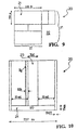
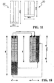
    1. A method for optimizing the occupation of circuit area in microcontroller electronic devices integrated on a semiconductor and incorporating macrocells and at least one memory matrix organized into rows and columns of cells, the number of columns defining the matrix height, the method being characterised by the following steps:
      defining the height (X) of the memory matrix (10) according to a number of memory address bits intended for selecting the row and column of the matrix, the width (Y) of said matrix being dependent on an overall desired capacity of the memory;
      deriving the selection of a memory location column from a predetermined number of least significant bits (A5÷A0) of the memory address bits;
      deriving the selection of a row from the remaining most significant bits (A15÷A6) of the memory address bits;
      utilising a predetermined number of addresses, referred to as the residuaries and having no corresponding locations in the memory, as additional matrix rows.
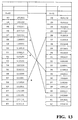
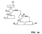
    2. A method according to Claim 1, characterized in that a pre-decoding step is- carried out on the memory address to check whether the codes of said predetermined number of bits (A5÷A0) relate to memory locations which belong to the set of residuaries, in conformity with the following rules:
      if the value of the least significant bit (A6) in the residuary row is 0, then the address relates to "even" rows and the bits of the predetermined number of bits (A5÷A0) undergo conversion by a complementation operation;
      if the value of the least significant bit (A6) in the residuary row is 1, then the address relates to "odd" rows, and the bits of the predetermined number of bits (A5÷A0) undergo conversion by a translation operation.
    EP97830239A 1996-10-17 1997-05-23 Method for optimising a memory cell matrix for a semiconductor integrated microcontroller Expired - Lifetime EP0837474B1 (en)

    Priority Applications (3)

    Application Number Priority Date Filing Date Title
    EP97830239A EP0837474B1 (en) 1996-10-17 1997-05-23 Method for optimising a memory cell matrix for a semiconductor integrated microcontroller
    US08/951,261 US6122702A (en) 1996-10-17 1997-10-16 Memory cells matrix for a semiconductor integrated microcontroller
    JP9285008A JPH10233093A (en) 1996-10-17 1997-10-17 Memory cell matrix for semiconductor integrated microcontroller

    Applications Claiming Priority (3)

    Application Number Priority Date Filing Date Title
    EP96830533 1996-10-17
    EP96830533 1996-10-17
    EP97830239A EP0837474B1 (en) 1996-10-17 1997-05-23 Method for optimising a memory cell matrix for a semiconductor integrated microcontroller

    Publications (3)

    Publication Number Publication Date
    EP0837474A2 EP0837474A2 (en) 1998-04-22
    EP0837474A3 EP0837474A3 (en) 1999-09-15
    EP0837474B1 true EP0837474B1 (en) 2005-02-02

    Family

    ID=26144344

    Family Applications (1)

    Application Number Title Priority Date Filing Date
    EP97830239A Expired - Lifetime EP0837474B1 (en) 1996-10-17 1997-05-23 Method for optimising a memory cell matrix for a semiconductor integrated microcontroller

    Country Status (3)

    Country Link
    US (1) US6122702A (en)
    EP (1) EP0837474B1 (en)
    JP (1) JPH10233093A (en)

    Families Citing this family (5)

    * Cited by examiner, † Cited by third party
    Publication number Priority date Publication date Assignee Title
    US6801981B1 (en) * 2000-06-14 2004-10-05 Netlogic Microsystems, Inc. Intra-row configurability of content addressable memory
    US6751701B1 (en) * 2000-06-14 2004-06-15 Netlogic Microsystems, Inc. Method and apparatus for detecting a multiple match in an intra-row configurable CAM system
    US6799243B1 (en) * 2000-06-14 2004-09-28 Netlogic Microsystems, Inc. Method and apparatus for detecting a match in an intra-row configurable cam system
    US6813680B1 (en) * 2000-06-14 2004-11-02 Netlogic Microsystems, Inc. Method and apparatus for loading comparand data into a content addressable memory system
    US6795892B1 (en) * 2000-06-14 2004-09-21 Netlogic Microsystems, Inc. Method and apparatus for determining a match address in an intra-row configurable cam device

    Family Cites Families (13)

    * Cited by examiner, † Cited by third party
    Publication number Priority date Publication date Assignee Title
    JPS5171648A (en) * 1974-12-18 1976-06-21 Panafacom Ltd
    US5633726A (en) * 1990-09-19 1997-05-27 U.S. Philips Corporation Digitized picture display system with added control files
    US5448710A (en) * 1991-02-26 1995-09-05 Hewlett-Packard Company Dynamically configurable interface cards with variable memory size
    US5404474A (en) * 1992-01-10 1995-04-04 Digital Equipment Corporation Apparatus and method for addressing a variable sized block of memory
    US5829007A (en) * 1993-06-24 1998-10-27 Discovision Associates Technique for implementing a swing buffer in a memory array
    US5396608A (en) * 1993-06-28 1995-03-07 Analog Devices, Inc. Method and apparatus for accessing variable length words in a memory array
    CA2145379C (en) * 1994-03-24 1999-06-08 William P. Robbins Method and apparatus for addressing memory
    US5689195A (en) * 1995-05-17 1997-11-18 Altera Corporation Programmable logic array integrated circuit devices
    US5860076A (en) * 1996-01-11 1999-01-12 Alliance Semiconductor Corporation 48-bit wide memory architecture addressing scheme reconfigurable for 8-bit, 16-bit and 32-bit data accesses
    US5736771A (en) * 1996-02-07 1998-04-07 United Microelectronics Corporation Mask ROM cell structure with multi-level data selection by code
    US5835502A (en) * 1996-06-28 1998-11-10 International Business Machines Corporation Method and apparatus for handling variable data word widths and array depths in a serial shared abist scheme
    US5844854A (en) * 1996-09-18 1998-12-01 Altera Corporation Programmable logic device with two dimensional memory addressing
    US5812472A (en) * 1997-07-16 1998-09-22 Tanisys Technology, Inc. Nested loop method of identifying synchronous memories

    Also Published As

    Publication number Publication date
    US6122702A (en) 2000-09-19
    EP0837474A3 (en) 1999-09-15
    JPH10233093A (en) 1998-09-02
    EP0837474A2 (en) 1998-04-22

    Similar Documents

    Publication Publication Date Title
    US4964078A (en) Combined multiple memories
    US5337267A (en) Squaring circuit for binary numbers
    US6381669B1 (en) Multi-bank, fault-tolerant, high-performance memory addressing system and method
    US5867422A (en) Computer memory chip with field programmable memory cell arrays (fpmcas), and method of configuring
    US5854763A (en) Integrated circuit with non-binary decoding and data access
    US4561072A (en) Memory system handling a plurality of bits as a unit to be processed
    US6748480B2 (en) Multi-bank, fault-tolerant, high-performance memory addressing system and method
    EP0394436A1 (en) Automatically variable memory interleaving system.
    US5572692A (en) Memory configuration decoding system having automatic row base address generation mechanism for variable memory devices with row access interleaving
    US5276827A (en) Data buffer for the duration of cyclically recurrent buffer periods
    CN112445455A (en) Memory read of weight values
    EP0303009A2 (en) Signal generator for circular addressing
    EP0837474B1 (en) Method for optimising a memory cell matrix for a semiconductor integrated microcontroller
    JPS6231440B2 (en)
    US20080301400A1 (en) Method and Arrangement for Efficiently Accessing Matrix Elements in a Memory
    JPH05282437A (en) Picture rotating circuit
    JPS6381688A (en) Semiconductor memory device
    KR0136534B1 (en) Semiconductor memory device
    JP3304632B2 (en) Interleaving method and interleaving circuit
    US6742077B1 (en) System for accessing a memory comprising interleaved memory modules having different capacities
    US7852705B1 (en) Method of and circuit for configuring a plurality of memory elements
    US20030031072A1 (en) Memory with row-wise write and column-wise read
    US5130923A (en) Selective dynamic RAM address generator with provision for automatic refresh
    US5737768A (en) Method and system for storing data blocks in a memory device
    JPH0661870A (en) Variable length coder decoder

    Legal Events

    Date Code Title Description
    PUAI Public reference made under article 153(3) epc to a published international application that has entered the european phase

    Free format text: ORIGINAL CODE: 0009012

    AK Designated contracting states

    Kind code of ref document: A2

    Designated state(s): DE FR GB IT

    RAP3 Party data changed (applicant data changed or rights of an application transferred)

    Owner name: STMICROELECTRONICS S.R.L.

    PUAL Search report despatched

    Free format text: ORIGINAL CODE: 0009013

    AK Designated contracting states

    Kind code of ref document: A3

    Designated state(s): AT BE CH DE DK ES FI FR GB GR IE IT LI LU MC NL PT SE

    17P Request for examination filed

    Effective date: 20000117

    AKX Designation fees paid

    Free format text: DE FR GB IT

    17Q First examination report despatched

    Effective date: 20020416

    GRAP Despatch of communication of intention to grant a patent

    Free format text: ORIGINAL CODE: EPIDOSNIGR1

    RTI1 Title (correction)

    Free format text: METHOD FOR OPTIMISING A MEMORY CELL MATRIX FOR A SEMICONDUCTOR INTEGRATED MICROCONTROLLER

    GRAS Grant fee paid

    Free format text: ORIGINAL CODE: EPIDOSNIGR3

    GRAA (expected) grant

    Free format text: ORIGINAL CODE: 0009210

    AK Designated contracting states

    Kind code of ref document: B1

    Designated state(s): DE FR GB IT

    REG Reference to a national code

    Ref country code: GB

    Ref legal event code: FG4D

    REF Corresponds to:

    Ref document number: 69732399

    Country of ref document: DE

    Date of ref document: 20050310

    Kind code of ref document: P

    PG25 Lapsed in a contracting state [announced via postgrant information from national office to epo]

    Ref country code: DE

    Free format text: LAPSE BECAUSE OF FAILURE TO SUBMIT A TRANSLATION OF THE DESCRIPTION OR TO PAY THE FEE WITHIN THE PRESCRIBED TIME-LIMIT

    Effective date: 20050503

    PLBE No opposition filed within time limit

    Free format text: ORIGINAL CODE: 0009261

    STAA Information on the status of an ep patent application or granted ep patent

    Free format text: STATUS: NO OPPOSITION FILED WITHIN TIME LIMIT

    26N No opposition filed

    Effective date: 20051103

    ET Fr: translation filed
    PGFP Annual fee paid to national office [announced via postgrant information from national office to epo]

    Ref country code: IT

    Payment date: 20060531

    Year of fee payment: 10

    PGFP Annual fee paid to national office [announced via postgrant information from national office to epo]

    Ref country code: GB

    Payment date: 20070427

    Year of fee payment: 11

    PGFP Annual fee paid to national office [announced via postgrant information from national office to epo]

    Ref country code: FR

    Payment date: 20070529

    Year of fee payment: 11

    GBPC Gb: european patent ceased through non-payment of renewal fee

    Effective date: 20080523

    REG Reference to a national code

    Ref country code: FR

    Ref legal event code: ST

    Effective date: 20090119

    PG25 Lapsed in a contracting state [announced via postgrant information from national office to epo]

    Ref country code: FR

    Free format text: LAPSE BECAUSE OF NON-PAYMENT OF DUE FEES

    Effective date: 20080602

    PG25 Lapsed in a contracting state [announced via postgrant information from national office to epo]

    Ref country code: GB

    Free format text: LAPSE BECAUSE OF NON-PAYMENT OF DUE FEES

    Effective date: 20080523

    PG25 Lapsed in a contracting state [announced via postgrant information from national office to epo]

    Ref country code: IT

    Free format text: LAPSE BECAUSE OF NON-PAYMENT OF DUE FEES

    Effective date: 20070523