EP0829360A2 - Method and materials for fabricating an ink-jet printhead - Google Patents
Method and materials for fabricating an ink-jet printhead Download PDFInfo
- Publication number
- EP0829360A2 EP0829360A2 EP97306996A EP97306996A EP0829360A2 EP 0829360 A2 EP0829360 A2 EP 0829360A2 EP 97306996 A EP97306996 A EP 97306996A EP 97306996 A EP97306996 A EP 97306996A EP 0829360 A2 EP0829360 A2 EP 0829360A2
- Authority
- EP
- European Patent Office
- Prior art keywords
- sacrificial layer
- layer
- depositing
- permanent
- ink
- Prior art date
- Legal status (The legal status is an assumption and is not a legal conclusion. Google has not performed a legal analysis and makes no representation as to the accuracy of the status listed.)
- Granted
Links
- 238000000034 method Methods 0.000 title claims abstract description 48
- 239000000463 material Substances 0.000 title claims abstract description 37
- 239000004642 Polyimide Substances 0.000 claims abstract description 16
- 229920001721 polyimide Polymers 0.000 claims abstract description 16
- 238000004519 manufacturing process Methods 0.000 claims abstract description 11
- RTZKZFJDLAIYFH-UHFFFAOYSA-N Diethyl ether Chemical compound CCOCC RTZKZFJDLAIYFH-UHFFFAOYSA-N 0.000 claims abstract description 9
- 238000005498 polishing Methods 0.000 claims abstract description 4
- 229920000412 polyarylene Polymers 0.000 claims abstract description 4
- 239000000758 substrate Substances 0.000 claims description 19
- 238000010438 heat treatment Methods 0.000 claims description 14
- 238000000151 deposition Methods 0.000 claims description 13
- -1 polyphenylene Polymers 0.000 claims description 7
- KJFMBFZCATUALV-UHFFFAOYSA-N phenolphthalein Chemical compound C1=CC(O)=CC=C1C1(C=2C=CC(O)=CC=2)C2=CC=CC=C2C(=O)O1 KJFMBFZCATUALV-UHFFFAOYSA-N 0.000 claims description 4
- BGTFCAQCKWKTRL-YDEUACAXSA-N chembl1095986 Chemical compound C1[C@@H](N)[C@@H](O)[C@H](C)O[C@H]1O[C@@H]([C@H]1C(N[C@H](C2=CC(O)=CC(O[C@@H]3[C@H]([C@@H](O)[C@H](O)[C@@H](CO)O3)O)=C2C=2C(O)=CC=C(C=2)[C@@H](NC(=O)[C@@H]2NC(=O)[C@@H]3C=4C=C(C(=C(O)C=4)C)OC=4C(O)=CC=C(C=4)[C@@H](N)C(=O)N[C@@H](C(=O)N3)[C@H](O)C=3C=CC(O4)=CC=3)C(=O)N1)C(O)=O)=O)C(C=C1)=CC=C1OC1=C(O[C@@H]3[C@H]([C@H](O)[C@@H](O)[C@H](CO[C@@H]5[C@H]([C@@H](O)[C@H](O)[C@@H](C)O5)O)O3)O[C@@H]3[C@H]([C@@H](O)[C@H](O)[C@@H](CO)O3)O[C@@H]3[C@H]([C@H](O)[C@@H](CO)O3)O)C4=CC2=C1 BGTFCAQCKWKTRL-YDEUACAXSA-N 0.000 claims description 2
- 239000011521 glass Substances 0.000 claims description 2
- 229910000679 solder Inorganic materials 0.000 claims description 2
- VYPSYNLAJGMNEJ-UHFFFAOYSA-N Silicium dioxide Chemical compound O=[Si]=O VYPSYNLAJGMNEJ-UHFFFAOYSA-N 0.000 claims 2
- 229920000265 Polyparaphenylene Polymers 0.000 claims 1
- 229910052581 Si3N4 Inorganic materials 0.000 claims 1
- UMIVXZPTRXBADB-UHFFFAOYSA-N benzocyclobutene Chemical compound C1=CC=C2CCC2=C1 UMIVXZPTRXBADB-UHFFFAOYSA-N 0.000 claims 1
- 150000004767 nitrides Chemical class 0.000 claims 1
- 235000012239 silicon dioxide Nutrition 0.000 claims 1
- 239000000377 silicon dioxide Substances 0.000 claims 1
- 239000007788 liquid Substances 0.000 abstract description 9
- XUIMIQQOPSSXEZ-UHFFFAOYSA-N Silicon Chemical compound [Si] XUIMIQQOPSSXEZ-UHFFFAOYSA-N 0.000 abstract description 7
- 229910052710 silicon Inorganic materials 0.000 abstract description 7
- 239000010703 silicon Substances 0.000 abstract description 7
- 239000011800 void material Substances 0.000 abstract description 2
- 239000010410 layer Substances 0.000 description 80
- 239000000976 ink Substances 0.000 description 26
- 229920000642 polymer Polymers 0.000 description 17
- 239000004065 semiconductor Substances 0.000 description 13
- 238000005530 etching Methods 0.000 description 11
- 230000015572 biosynthetic process Effects 0.000 description 9
- 238000003786 synthesis reaction Methods 0.000 description 8
- 238000007641 inkjet printing Methods 0.000 description 6
- 239000000126 substance Substances 0.000 description 5
- 238000012512 characterization method Methods 0.000 description 4
- 125000003118 aryl group Chemical group 0.000 description 3
- 238000003486 chemical etching Methods 0.000 description 3
- 229920002521 macromolecule Polymers 0.000 description 3
- 239000002184 metal Substances 0.000 description 3
- 229910052751 metal Inorganic materials 0.000 description 3
- 229920002120 photoresistant polymer Polymers 0.000 description 3
- 230000008569 process Effects 0.000 description 3
- PXHVJJICTQNCMI-UHFFFAOYSA-N Nickel Chemical compound [Ni] PXHVJJICTQNCMI-UHFFFAOYSA-N 0.000 description 2
- PPBRXRYQALVLMV-UHFFFAOYSA-N Styrene Chemical compound C=CC1=CC=CC=C1 PPBRXRYQALVLMV-UHFFFAOYSA-N 0.000 description 2
- 239000000919 ceramic Substances 0.000 description 2
- 230000008878 coupling Effects 0.000 description 2
- 238000010168 coupling process Methods 0.000 description 2
- 238000005859 coupling reaction Methods 0.000 description 2
- 230000000694 effects Effects 0.000 description 2
- 238000005516 engineering process Methods 0.000 description 2
- 230000006911 nucleation Effects 0.000 description 2
- 238000010899 nucleation Methods 0.000 description 2
- 230000000269 nucleophilic effect Effects 0.000 description 2
- 229920001643 poly(ether ketone) Polymers 0.000 description 2
- 230000000717 retained effect Effects 0.000 description 2
- 239000004793 Polystyrene Substances 0.000 description 1
- 238000002679 ablation Methods 0.000 description 1
- 239000002253 acid Substances 0.000 description 1
- 230000003213 activating effect Effects 0.000 description 1
- 125000003178 carboxy group Chemical group [H]OC(*)=O 0.000 description 1
- 230000015556 catabolic process Effects 0.000 description 1
- 238000006243 chemical reaction Methods 0.000 description 1
- 210000001072 colon Anatomy 0.000 description 1
- 239000004020 conductor Substances 0.000 description 1
- 239000013078 crystal Substances 0.000 description 1
- 230000003247 decreasing effect Effects 0.000 description 1
- 238000006731 degradation reaction Methods 0.000 description 1
- 230000008021 deposition Effects 0.000 description 1
- 238000001035 drying Methods 0.000 description 1
- 150000002170 ethers Chemical class 0.000 description 1
- 239000010408 film Substances 0.000 description 1
- 229920000578 graft copolymer Polymers 0.000 description 1
- 229920006158 high molecular weight polymer Polymers 0.000 description 1
- 238000010849 ion bombardment Methods 0.000 description 1
- 238000000608 laser ablation Methods 0.000 description 1
- 238000010329 laser etching Methods 0.000 description 1
- 238000002356 laser light scattering Methods 0.000 description 1
- 230000014759 maintenance of location Effects 0.000 description 1
- 230000007246 mechanism Effects 0.000 description 1
- 238000005459 micromachining Methods 0.000 description 1
- 239000000203 mixture Substances 0.000 description 1
- 229910052759 nickel Inorganic materials 0.000 description 1
- 238000000059 patterning Methods 0.000 description 1
- 229920002852 poly(2,6-dimethyl-1,4-phenylene oxide) polymer Polymers 0.000 description 1
- 229920002492 poly(sulfone) Polymers 0.000 description 1
- 229920001230 polyarylate Polymers 0.000 description 1
- 229920006260 polyaryletherketone Polymers 0.000 description 1
- 229910021420 polycrystalline silicon Inorganic materials 0.000 description 1
- 238000006116 polymerization reaction Methods 0.000 description 1
- 229920005591 polysilicon Polymers 0.000 description 1
- 229920002223 polystyrene Polymers 0.000 description 1
- 238000002360 preparation method Methods 0.000 description 1
- 239000011347 resin Substances 0.000 description 1
- 229920005989 resin Polymers 0.000 description 1
- 230000004044 response Effects 0.000 description 1
- 238000007650 screen-printing Methods 0.000 description 1
- 239000002356 single layer Substances 0.000 description 1
- 239000007787 solid Substances 0.000 description 1
- 238000004528 spin coating Methods 0.000 description 1
- 238000005507 spraying Methods 0.000 description 1
- 230000003068 static effect Effects 0.000 description 1
- 238000001370 static light scattering Methods 0.000 description 1
- 229920001169 thermoplastic Polymers 0.000 description 1
- 239000004416 thermosoftening plastic Substances 0.000 description 1
- 239000010409 thin film Substances 0.000 description 1
- 238000009834 vaporization Methods 0.000 description 1
- 230000008016 vaporization Effects 0.000 description 1
Images


Classifications
-
- B—PERFORMING OPERATIONS; TRANSPORTING
- B41—PRINTING; LINING MACHINES; TYPEWRITERS; STAMPS
- B41J—TYPEWRITERS; SELECTIVE PRINTING MECHANISMS, i.e. MECHANISMS PRINTING OTHERWISE THAN FROM A FORME; CORRECTION OF TYPOGRAPHICAL ERRORS
- B41J2/00—Typewriters or selective printing mechanisms characterised by the printing or marking process for which they are designed
- B41J2/005—Typewriters or selective printing mechanisms characterised by the printing or marking process for which they are designed characterised by bringing liquid or particles selectively into contact with a printing material
- B41J2/01—Ink jet
- B41J2/135—Nozzles
- B41J2/16—Production of nozzles
- B41J2/1621—Manufacturing processes
- B41J2/1637—Manufacturing processes molding
- B41J2/1639—Manufacturing processes molding sacrificial molding
-
- B—PERFORMING OPERATIONS; TRANSPORTING
- B41—PRINTING; LINING MACHINES; TYPEWRITERS; STAMPS
- B41J—TYPEWRITERS; SELECTIVE PRINTING MECHANISMS, i.e. MECHANISMS PRINTING OTHERWISE THAN FROM A FORME; CORRECTION OF TYPOGRAPHICAL ERRORS
- B41J2/00—Typewriters or selective printing mechanisms characterised by the printing or marking process for which they are designed
- B41J2/005—Typewriters or selective printing mechanisms characterised by the printing or marking process for which they are designed characterised by bringing liquid or particles selectively into contact with a printing material
- B41J2/01—Ink jet
- B41J2/135—Nozzles
- B41J2/16—Production of nozzles
- B41J2/1601—Production of bubble jet print heads
-
- B—PERFORMING OPERATIONS; TRANSPORTING
- B41—PRINTING; LINING MACHINES; TYPEWRITERS; STAMPS
- B41J—TYPEWRITERS; SELECTIVE PRINTING MECHANISMS, i.e. MECHANISMS PRINTING OTHERWISE THAN FROM A FORME; CORRECTION OF TYPOGRAPHICAL ERRORS
- B41J2/00—Typewriters or selective printing mechanisms characterised by the printing or marking process for which they are designed
- B41J2/005—Typewriters or selective printing mechanisms characterised by the printing or marking process for which they are designed characterised by bringing liquid or particles selectively into contact with a printing material
- B41J2/01—Ink jet
- B41J2/135—Nozzles
- B41J2/16—Production of nozzles
- B41J2/1607—Production of print heads with piezoelectric elements
-
- B—PERFORMING OPERATIONS; TRANSPORTING
- B41—PRINTING; LINING MACHINES; TYPEWRITERS; STAMPS
- B41J—TYPEWRITERS; SELECTIVE PRINTING MECHANISMS, i.e. MECHANISMS PRINTING OTHERWISE THAN FROM A FORME; CORRECTION OF TYPOGRAPHICAL ERRORS
- B41J2/00—Typewriters or selective printing mechanisms characterised by the printing or marking process for which they are designed
- B41J2/005—Typewriters or selective printing mechanisms characterised by the printing or marking process for which they are designed characterised by bringing liquid or particles selectively into contact with a printing material
- B41J2/01—Ink jet
- B41J2/135—Nozzles
- B41J2/16—Production of nozzles
- B41J2/1621—Manufacturing processes
- B41J2/1626—Manufacturing processes etching
- B41J2/1628—Manufacturing processes etching dry etching
-
- B—PERFORMING OPERATIONS; TRANSPORTING
- B41—PRINTING; LINING MACHINES; TYPEWRITERS; STAMPS
- B41J—TYPEWRITERS; SELECTIVE PRINTING MECHANISMS, i.e. MECHANISMS PRINTING OTHERWISE THAN FROM A FORME; CORRECTION OF TYPOGRAPHICAL ERRORS
- B41J2/00—Typewriters or selective printing mechanisms characterised by the printing or marking process for which they are designed
- B41J2/005—Typewriters or selective printing mechanisms characterised by the printing or marking process for which they are designed characterised by bringing liquid or particles selectively into contact with a printing material
- B41J2/01—Ink jet
- B41J2/135—Nozzles
- B41J2/16—Production of nozzles
- B41J2/1621—Manufacturing processes
- B41J2/1626—Manufacturing processes etching
- B41J2/1629—Manufacturing processes etching wet etching
-
- B—PERFORMING OPERATIONS; TRANSPORTING
- B41—PRINTING; LINING MACHINES; TYPEWRITERS; STAMPS
- B41J—TYPEWRITERS; SELECTIVE PRINTING MECHANISMS, i.e. MECHANISMS PRINTING OTHERWISE THAN FROM A FORME; CORRECTION OF TYPOGRAPHICAL ERRORS
- B41J2/00—Typewriters or selective printing mechanisms characterised by the printing or marking process for which they are designed
- B41J2/005—Typewriters or selective printing mechanisms characterised by the printing or marking process for which they are designed characterised by bringing liquid or particles selectively into contact with a printing material
- B41J2/01—Ink jet
- B41J2/135—Nozzles
- B41J2/16—Production of nozzles
- B41J2/1621—Manufacturing processes
- B41J2/1631—Manufacturing processes photolithography
-
- B—PERFORMING OPERATIONS; TRANSPORTING
- B41—PRINTING; LINING MACHINES; TYPEWRITERS; STAMPS
- B41J—TYPEWRITERS; SELECTIVE PRINTING MECHANISMS, i.e. MECHANISMS PRINTING OTHERWISE THAN FROM A FORME; CORRECTION OF TYPOGRAPHICAL ERRORS
- B41J2/00—Typewriters or selective printing mechanisms characterised by the printing or marking process for which they are designed
- B41J2/005—Typewriters or selective printing mechanisms characterised by the printing or marking process for which they are designed characterised by bringing liquid or particles selectively into contact with a printing material
- B41J2/01—Ink jet
- B41J2/135—Nozzles
- B41J2/16—Production of nozzles
- B41J2/1621—Manufacturing processes
- B41J2/1632—Manufacturing processes machining
- B41J2/1634—Manufacturing processes machining laser machining
-
- B—PERFORMING OPERATIONS; TRANSPORTING
- B41—PRINTING; LINING MACHINES; TYPEWRITERS; STAMPS
- B41J—TYPEWRITERS; SELECTIVE PRINTING MECHANISMS, i.e. MECHANISMS PRINTING OTHERWISE THAN FROM A FORME; CORRECTION OF TYPOGRAPHICAL ERRORS
- B41J2/00—Typewriters or selective printing mechanisms characterised by the printing or marking process for which they are designed
- B41J2/005—Typewriters or selective printing mechanisms characterised by the printing or marking process for which they are designed characterised by bringing liquid or particles selectively into contact with a printing material
- B41J2/01—Ink jet
- B41J2/135—Nozzles
- B41J2/16—Production of nozzles
- B41J2/1621—Manufacturing processes
- B41J2/1635—Manufacturing processes dividing the wafer into individual chips
-
- B—PERFORMING OPERATIONS; TRANSPORTING
- B41—PRINTING; LINING MACHINES; TYPEWRITERS; STAMPS
- B41J—TYPEWRITERS; SELECTIVE PRINTING MECHANISMS, i.e. MECHANISMS PRINTING OTHERWISE THAN FROM A FORME; CORRECTION OF TYPOGRAPHICAL ERRORS
- B41J2/00—Typewriters or selective printing mechanisms characterised by the printing or marking process for which they are designed
- B41J2/005—Typewriters or selective printing mechanisms characterised by the printing or marking process for which they are designed characterised by bringing liquid or particles selectively into contact with a printing material
- B41J2/01—Ink jet
- B41J2/135—Nozzles
- B41J2/16—Production of nozzles
- B41J2/1621—Manufacturing processes
- B41J2/164—Manufacturing processes thin film formation
- B41J2/1642—Manufacturing processes thin film formation thin film formation by CVD [chemical vapor deposition]
-
- B—PERFORMING OPERATIONS; TRANSPORTING
- B41—PRINTING; LINING MACHINES; TYPEWRITERS; STAMPS
- B41J—TYPEWRITERS; SELECTIVE PRINTING MECHANISMS, i.e. MECHANISMS PRINTING OTHERWISE THAN FROM A FORME; CORRECTION OF TYPOGRAPHICAL ERRORS
- B41J2/00—Typewriters or selective printing mechanisms characterised by the printing or marking process for which they are designed
- B41J2/005—Typewriters or selective printing mechanisms characterised by the printing or marking process for which they are designed characterised by bringing liquid or particles selectively into contact with a printing material
- B41J2/01—Ink jet
- B41J2/135—Nozzles
- B41J2/16—Production of nozzles
- B41J2/1621—Manufacturing processes
- B41J2/164—Manufacturing processes thin film formation
- B41J2/1645—Manufacturing processes thin film formation thin film formation by spincoating
-
- B—PERFORMING OPERATIONS; TRANSPORTING
- B41—PRINTING; LINING MACHINES; TYPEWRITERS; STAMPS
- B41J—TYPEWRITERS; SELECTIVE PRINTING MECHANISMS, i.e. MECHANISMS PRINTING OTHERWISE THAN FROM A FORME; CORRECTION OF TYPOGRAPHICAL ERRORS
- B41J2202/00—Embodiments of or processes related to ink-jet or thermal heads
- B41J2202/01—Embodiments of or processes related to ink-jet heads
- B41J2202/03—Specific materials used
Definitions
- the present invention relates to techniques and special materials for fabricating micromechanical devices, particularly ink-jet printheads, and to an ink-jet printhead made according to this technique.
- droplets of ink are selectably ejected from a plurality of drop ejectors in a printhead.
- the ejectors are operated in accordance with digital instructions to create a desired image on a print sheet moving past the printhead.
- the printhead may move back and forth relative to the sheet in a typewriter fashion, or the linear array may be of a size extending across the entire width of a sheet, to place the image on a sheet in a single pass.
- the ejectors typically comprise capillary channels, or other ink passageways, which are connected to one or more common ink supply manifolds. Ink is retained within each channel until, in response to an appropriate digital signal, the ink in the channel is rapidly heated and vaporized by a heating element (essentially a resistor) disposed on a surface within the channel. This rapid vaporization of the ink adjacent the channel creates a bubble which causes a quantity of ink to be ejected through an opening associated with the channel to the print sheet.
- a heating element essentially a resistor
- a thermal ink-jet printhead such as of typical designs known in the art is a hybrid of a semiconductor and a micromechanical device.
- the heating elements are typically polysilicon regions doped to a particular resistivity, and the associated digital circuits for activating individual heating elements at various times are all well within the realm of semiconductor technology.
- structures such as the capillary channels for retaining liquid ink and ejecting the ink from the printhead are mechanical structures which directly physically interface with the semiconductors such as the heating element or heater chip. For various reasons it is desirable to make mechanical structures such as the channel plate out of chemically etched silicon which is congruous with the semiconductor structure of the heater plate.
- V-groove etching such as by applying a chemical etchant such as KOH to silicon. Because of the relative etching rates along different directions of a silicon crystal (the "aspect ratio"), etched cavities defining specific surface angles will result, forming the distinct V-grooves.
- a channel plate defining etched V-grooves is abutted against a semiconductor heater chip, capillary channels which are triangular in cross-section are created.
- Such triangular cross-sections provide certain advantages, but are known to exhibit problems in directionality of ink droplets emitted therefrom; i.e., ink droplets are not always emitted straight out of the channel, but rather may be emitted at an unpredictable angle. It is likely that the performance of the chip could otherwise be improved if, for example, a cross-section which is closer to a square could be provided. However, the aspect ratio for the etching of silicon in typical etching processes would preclude creation of square-shaped grooves in a channel plate.
- V-grooves to form capillary channels
- V-groove etching Another disadvantage of using V-grooves to form capillary channels is that it would be difficult to create, using V-groove etching, a channel which would vary in cross-section along the length of the channel. It would be difficult, for example, to create through V-groove etching a channel which increased or decreased in size along its length.
- V-groove etching technique has key practical advantages, there are also important design constraints associated with it.
- the present invention describes a method, along with associated sets of material with which the method is preferably practiced, by which structures such as are useful in an ink-jet printhead can be created with more flexibility than with traditional V-groove etching techniques.
- US-A-4,497,684 discloses a technique, using sacrificial layers, to deposit metal layers in a pattern on a substrate.
- US-A-4,650,545 discloses a technique for making metal conductors which adhere to polyimide layers.
- US-A-5,236,572 discloses a method for continuously manufacturing parts requiring precision micro-fabrication, such as ink-jet printheads.
- US-A-5,296,092 discloses a planarization method for use with a semiconductor substrate.
- US-A-5,322,594 discloses a method of manufacturing a one piece full-width ink-jet printing bar on a glass or ceramic plate.
- US-A-5,378,583 discloses a technique for forming microstructures using a preformed sheet of photoresist.
- US-A-5,401,983 discloses various techniques for monolithically integrating any thin film material or any device, including semiconductors.
- US-A-5,454,904 discloses a micromachining method wherein a polyimide is utilized as a micromachinable material.
- US-A-5,465,009 discloses techniques to permit lift-off, alignment and bonding of materials and devices.
- a device layer is deposited on a sacrificial layer situation on a growth substrate.
- the device layer is coated with a carrier layer.
- the sacrificial layer and/or the growth substrate are then etched away to release the combination of the device layer and carrier layer from the growth substrate.
- a method of fabricating a micromechanical device defining a cavity therein such as an ink-jet printhead.
- a substrate defining a main surface is provided.
- a sacrificial layer of removable material, configured as a negative mold of the desired cavity, is deposited on the main surface.
- a permanent layer of permanent material is deposited over the main surface and the sacrificial layer. The permanent layer is polished to expose the sacrificial layer, and then the sacrificial layer is removed.
- Figures 1-5 show a plan view of a portion of a semiconductor substrate having structures thereon, as would be used, for example, in creating a portion of a thermal ink-jet printhead.
- the successive Figures show the different steps in the method according to the present invention.
- like reference numerals indicate the same element at different stages in the process.
- Figure 1 shows a semiconductor substrate 10 having disposed, on a main surface thereof, a series of sacrificial portions 12, which together can be construed as a single sacrificial layer.
- the individual sacrificial portions 12 are intended to represent a set of capillary channels for the passage of liquid ink therethrough in, for example, a thermal ink-jet printhead.
- the sacrificial portions 12 represent the configuration of voids (such as for capillary channels) in the finished printhead; the portions 12 can be construed as forming a negative of a mold.
- these capillary channels are intended to be disposed on the main surface of chip 10, in such a manner that the main surface of chip 10 serves as one wall of each capillary channel.
- four separate and parallel channels are shown "end-on.”
- the sacrificial layer 12 can be deposited in a desired pattern on the main surface of chip 10 using any number of a familiar techniques, such as laser etching, chemical etching, or photoresist etching.
- FIG 2 is shown the placement of a permanent layer 14 over the portions 12 of the sacrificial layer.
- Permanent layer 14 will ultimately be used to define the voids which, in Figure 2, are occupied by sacrificial layers 12. It will be noted that, in the illustrated embodiment, the parallel-channel pattern of sacrificial layer 12 causes an undulating surface to be created by permanent layer 14.
- the permanent layer 14 can be deposited by any number of available techniques, such as spin casting, spray coating, screen printing, CVD or plasma deposition. A detailed discussion of what materials are most suited for permanent layer 14 will be given below.
- the permanent layer 14 which has been hardened to a solid, has been mechanically polished in such a manner that a single flat surface is obtained, with different areas thereof being formed by portions of permanent layer 14 or exposed portions of sacrificial layer 12.
- this polishing step can be carried out by any of a variety of known techniques, such as mechanical polishing or laser ablation.
- the sacrificial layer represented in previous Figures by portions 12, has been removed. According to a preferred embodiment of the present invention, this removal of sacrificial layer 12 is carried out by chemical etching, although other techniques may be possible. It can be seen that there are now precisely-shaped channels where the sacrificial layers 12 used to be. These channels can in turn be used for passage and retention of liquid ink, such as a thermal ink-jet printhead. It will further be noted that substantially right angles can be provided between the walls of permanent layer 14 and the "floor" formed by the main surface of chip 10 within each channel. This is shown in contrast to previous typical designs of ink-jet printheads, using V-groove etching, wherein only triangular-cross-section channels are practical.
- Figure 5 shows a possible subsequent step in the process of the present invention, wherein further structures can be provided on the remaining portions of the permanent layer 14.
- a second sacrificial layer 16 can be placed in various ways over the permanent layer 14, such as by placing the sacrificial layer 16 entirely over a portion of permanent layer 14, or else, as shown toward the right of Figure 5, placing a portion of the sacrificial layer 16 over permanent layer 14 or over the remaining exposed main surface of chip 10.
- the steps shown in Figures 1-4 can thus be repeated over the existing permanent layers 14 in order to create fairly sophisticated three-dimensional structures.
- multiple permanent layers of the same general plan design can be "stacked" on top of each other, thereby creating "trenches" having a high aspect ratio of height to width.
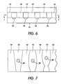
- Figure 6 is an elevational view of a substantially finished ink-jet printhead exploiting, for example, the structure shown in Figure 4.
- the semiconductor substrate 10 has defined therein (such as through semiconductor fabrication means known in the art) a series of heating elements 24 on which the channels formed by permanent layer 14 are aligned.
- a voltage to a heating element such as 24 will cause nucleation of the liquid ink being retained in the channel, which in turn causes the liquid ink to be ejected from the channel and onto a print sheet.
- the heating element 24 could be replaced with another kind of structure to energize the liquid ink and cause ejection of ink from the channel, such as a piezoelectric structure; in the claims hereinbelow, a heating or other structure is generalized as an "energizing surface."
- a simple plane layer 20 Disposed over the "top" surface provided by permanent layer 14 is a simple plane layer 20, which in effect completes the channels formed by semiconductor substrate 10 and the walls of permanent layer 14 so that enclosed (but open-ended) capillary channels are created.
- plane layer 20 need not have any particular sophisticated structure associated therewith, and can be made of an inexpensive ceramic, resin, or metal.
- Figure 7 is a plan view showing how the technique of the present invention can, by virtue of using permanent layer 14 to facilitate channel shapes which vary in cross-section along the length thereof, to an extent that is impossible with channels which are created in directly etched grooves.
- the channels are created by placing on the substrate sacrifical layers 12 which are shaped like the desired channels in the finished printhead.
- Figure 7 merely shows three possible examples of such odd-shaped channels: of course, all of the channels would be of the same general design in a practical printhead.
- the various possible shapes of the channels created by permanent layer 14 facilitate shapes which can be optimized relative to, for example, the position of the heating element 24 in semiconductor chip 10.
- FIG 8 is a perspective view of an ejector made according to the technique of the present invention, showing an important printhead design which can be readily enabled with the technique of the present invention.
- a heating element 24, such as shown in Figure 7, is defined within a heater chip 10
- permanent layer 14 can be used not only to define an ejector channel, but also to form a pit, indicated as 25, which is spaced around, or closely to, the perimeter of the surface of heating element 24.
- This pit 25 is known in the art as a structure which can improve the performance of a thermal ink-jet ejector by providing a specific zone for ink nucleation.
- pits such as 25 are formed in their own separate layers, such as a polyimide, which must be provided to the printhead chip in a separate manufacturing step.
- a structure defining a pit 25 around every heating element 24 can be formed in a single piece with the rest of the sides of the ejector, by permanent layer 14. That is, the present invention enables structure defining pit 25 to be formed out of essentially the same layer of material that defines the walls of the ejector itself. Formation of this pit 25 in permanent layer 14 can be performed by multiple iterations of the sacrificial layer technique as shown in Figure 5.
- the negative-mold technique is used for the creation of capillary channels in a thermal ink-jet printhead
- the technique can be used to form other types of cavities in a printhead, such as to make the ink-supply manifolds through which ink is supplied to the channels in the printhead.
- the technique of the present invention can be applied to making any specially-shaped void in a micromechanical apparatus, and can readily be applied to the creation of voids having a critical dimension (i.e. along a dimension parallel to the main surface of the substrate) from about 3 micrometers to about one centimeter.
- Figure 9 is a table giving, in general terms, various preferred combinations of sacrificial layer material, permanent layer material, sacrificial layer patterning methods, and dissolving chemicals, representing various practices of the invention known to the inventors as of the time of filing.
- the necessary attributes of a sacrificial material is that it be patternable (either by being photosensitive itself, or being patternable by the application of a photoresist), and removable (such as by wet or plasma chemical etching, ion bombardment, or ablation).
- different types of polyimide can be used respectively for the sacrificial and permanent layers. If two types of polyimide are used, the polyimide used for the sacrifical layer should be a partially-cured polyimide, while the polyimide for the permanent layer should be a fully-cured polyimide. Alternately, the polyimide used for sacrifical layer should be a base-sensitive polyimide, while the polyimide for the permanent layer should be a less base-sensitive polyimide.
- a single layer of permanent material 14 can be readily created up to a thickness of 60 micrometers. Such a layer will still exhibit the desirable right-angle relationship between the walls of the permanent layer such as 14 and the surface of the silicon substrate 10.
- the thickness of such a permanent layer 14 comprising several such layers could easily reach into the tens of millimeters.
- the thickness of structures created by one or more permanent layers 14 is fundamentally constrained only by the mechanical stability of such walls, i.e., a wall created by permanent layer 14 need only be thick enough to support itself in a particular situation.
Abstract
Description
Claims (10)
- A method of fabricating a micromechanical device defining a cavity therein, comprising the steps of:providing a substrate (10) defining a main surface;depositing on the main surface a sacrificial layer (12) of a first material, configured as a negative mold of the cavity;depositing over the sacrificial layer a permanent layer (14) of a second material;polishing the permanent layer (14) to expose the sacrificial layer (12); andremoving the sacrificial layer (12).
- The method of claim 1, wherein the substrate (10) defines a heating surface.
- The method of either of claims 1 or 2, wherein the step of depositing on the main surface a sacrificial layer (12) comprises the step of depositing the sacrificial layer (12) whereby edges of the sacrificial layer (12) form substantially right angles with the main surface of the substrate (10).
- The method of any of claims 1 to 3, comprising the further steps ofdepositing on the permanent layer (14) a second sacrifical layer (16); anddepositing over the second sacrificial layer (16) a second permanent layer.
- The method of any of claims 1 to 4, wherein a cavity formed as a negative mold in the sacrifical layer (12) has a dimension parallel to the main surface not less than about 3 micrometers and not more than about one centimeter.
- The method of any of claims 1 to 5, wherein said first material is selected from the group consisting of a dry-film solder mask, a plasma nitride, a plasma oxide, a spin-on glass, a polyimide, RISTON, and VACREL.
- The method of any of claims 1 to 6, wherein said second material is selected from the group consisting of a probimer, a benzocyclobutene, silicon dioxide, Si3N4, a polyphenylene, a polyarylene ether and a phenolphthalein containing arylene ether.
- A method of fabricating an ink-jet printhead defining a plurality of channels therein, comprising the steps of:providing a substrate (10) defining a main surface;depositing on the main surface a sacrificial layer (12) of a first material, configured as a negative mold of the plurality of channels;depositing over the sacrificial layer a permanent layer (14) of a second material; andremoving the sacrificial layer (12).
- The method of claim 8, the substrate (10) defining a plurality of energizing surfaces in the main surface thereof, each energizing surface corresponding to one channel in the printhead, and wherein the step of depositing on the main surface a sacrificial layer (12) comprises the step of depositing the sacrificial layer (12) over the energizing surface.
- The method of claim 9, wherein the step of depositing the sacrificial layer (12) includes depositing the sacrificial layer (12) within a perimeter (24) of the energizing surface, thereby allowing the permanent layer (14) to form a pit (25) around the perimeter (24) of the energizing surface.
Applications Claiming Priority (2)
| Application Number | Priority Date | Filing Date | Title |
|---|---|---|---|
| US712761 | 1996-09-12 | ||
| US08/712,761 US5738799A (en) | 1996-09-12 | 1996-09-12 | Method and materials for fabricating an ink-jet printhead |
Publications (3)
| Publication Number | Publication Date |
|---|---|
| EP0829360A2 true EP0829360A2 (en) | 1998-03-18 |
| EP0829360A3 EP0829360A3 (en) | 1999-08-18 |
| EP0829360B1 EP0829360B1 (en) | 2004-03-31 |
Family
ID=24863452
Family Applications (1)
| Application Number | Title | Priority Date | Filing Date |
|---|---|---|---|
| EP97306996A Expired - Lifetime EP0829360B1 (en) | 1996-09-12 | 1997-09-09 | Method and materials for fabricating an ink-jet printhead |
Country Status (4)
| Country | Link |
|---|---|
| US (1) | US5738799A (en) |
| EP (1) | EP0829360B1 (en) |
| JP (1) | JPH1086392A (en) |
| DE (1) | DE69728336T2 (en) |
Cited By (68)
| Publication number | Priority date | Publication date | Assignee | Title |
|---|---|---|---|---|
| GB2326619A (en) * | 1997-06-06 | 1998-12-30 | David Westberg | Edgeshooter bubble jet printer nozzle formed by etching of a sacrificial metallic layer |
| WO2000023279A1 (en) * | 1998-10-16 | 2000-04-27 | Silverbrook Research Pty. Limited | Improvements relating to inkjet printers |
| WO2001001025A2 (en) * | 1999-06-28 | 2001-01-04 | California Institute Of Technology | Microfabricated elastomeric valve and pump systems |
| US6832828B2 (en) | 1998-09-09 | 2004-12-21 | Silverbrook Research Pty Ltd | Micro-electromechanical fluid ejection device with control logic circuitry |
| US6863378B2 (en) | 1998-10-16 | 2005-03-08 | Silverbrook Research Pty Ltd | Inkjet printer having enclosed actuators |
| US6899137B2 (en) | 1999-06-28 | 2005-05-31 | California Institute Of Technology | Microfabricated elastomeric valve and pump systems |
| US6902255B1 (en) | 1998-10-16 | 2005-06-07 | Silverbrook Research Pty Ltd | Inkjet printers |
| US6913347B2 (en) | 1998-10-16 | 2005-07-05 | Silverbrook Research Pty Ltd | Inkjet printhead chip with trace orientation to enhance performance characteristics |
| US6929030B2 (en) | 1999-06-28 | 2005-08-16 | California Institute Of Technology | Microfabricated elastomeric valve and pump systems |
| US6938994B2 (en) | 1998-10-16 | 2005-09-06 | Silverbrook Research Pty Ltd | Method of operating an ink jet printhead within a predetermined temperature range |
| US6951632B2 (en) | 2000-11-16 | 2005-10-04 | Fluidigm Corporation | Microfluidic devices for introducing and dispensing fluids from microfluidic systems |
| US6994424B2 (en) | 1998-10-16 | 2006-02-07 | Silverbrook Research Pty Ltd | Printhead assembly incorporating an array of printhead chips on an ink distribution structure |
| US7001007B2 (en) | 1998-10-16 | 2006-02-21 | Silverbrook Research Pty Ltd | Method of ejecting liquid from a micro-electromechanical device |
| US7028474B2 (en) | 1998-10-16 | 2006-04-18 | Silverbook Research Pty Ltd | Micro-electromechanical actuator with control logic circuitry |
| US7032992B2 (en) | 1998-10-16 | 2006-04-25 | Silverbrook Research Pty Ltd | Inkjet printer using meniscus rim in nozzle chamber |
| US7080893B2 (en) | 1998-10-16 | 2006-07-25 | Silverbrook Research Pty Ltd | Ink jet printhead having columnar arrays of transistor drive circuits |
| US7097809B2 (en) | 2000-10-03 | 2006-08-29 | California Institute Of Technology | Combinatorial synthesis system |
| US7111924B2 (en) | 1998-10-16 | 2006-09-26 | Silverbrook Research Pty Ltd | Inkjet printhead having thermal bend actuator heating element electrically isolated from nozzle chamber ink |
| US7144616B1 (en) | 1999-06-28 | 2006-12-05 | California Institute Of Technology | Microfabricated elastomeric valve and pump systems |
| US7143785B2 (en) | 2002-09-25 | 2006-12-05 | California Institute Of Technology | Microfluidic large scale integration |
| US7182431B2 (en) | 1999-10-19 | 2007-02-27 | Silverbrook Research Pty Ltd | Nozzle arrangement |
| US7192629B2 (en) | 2001-10-11 | 2007-03-20 | California Institute Of Technology | Devices utilizing self-assembled gel and method of manufacture |
| US7195670B2 (en) | 2000-06-27 | 2007-03-27 | California Institute Of Technology | High throughput screening of crystallization of materials |
| US7217321B2 (en) | 2001-04-06 | 2007-05-15 | California Institute Of Technology | Microfluidic protein crystallography techniques |
| US7217367B2 (en) | 2001-04-06 | 2007-05-15 | Fluidigm Corporation | Microfluidic chromatography |
| US7232109B2 (en) | 2000-11-06 | 2007-06-19 | California Institute Of Technology | Electrostatic valves for microfluidic devices |
| US7237874B2 (en) | 2000-06-30 | 2007-07-03 | Silverbrook Research Pty Ltd | Inkjet printhead with grouped nozzles and a nozzle guard |
| US7244402B2 (en) | 2001-04-06 | 2007-07-17 | California Institute Of Technology | Microfluidic protein crystallography |
| US7258774B2 (en) | 2000-10-03 | 2007-08-21 | California Institute Of Technology | Microfluidic devices and methods of use |
| US7279146B2 (en) | 2003-04-17 | 2007-10-09 | Fluidigm Corporation | Crystal growth devices and systems, and methods for using same |
| US7291512B2 (en) | 2001-08-30 | 2007-11-06 | Fluidigm Corporation | Electrostatic/electrostrictive actuation of elastomer structures using compliant electrodes |
| US7294503B2 (en) | 2000-09-15 | 2007-11-13 | California Institute Of Technology | Microfabricated crossflow devices and methods |
| US7306672B2 (en) | 2001-04-06 | 2007-12-11 | California Institute Of Technology | Microfluidic free interface diffusion techniques |
| US7326296B2 (en) | 2001-04-06 | 2008-02-05 | California Institute Of Technology | High throughput screening of crystallization of materials |
| US7368163B2 (en) | 2001-04-06 | 2008-05-06 | Fluidigm Corporation | Polymer surface modification |
| US7380906B2 (en) | 1998-10-16 | 2008-06-03 | Silverbrook Research Pty Ltd | Printhead |
| US7384131B2 (en) | 1998-10-16 | 2008-06-10 | Silverbrook Research Pty Ltd | Pagewidth printhead having small print zone |
| US7407799B2 (en) | 2004-01-16 | 2008-08-05 | California Institute Of Technology | Microfluidic chemostat |
| US7419250B2 (en) | 1999-10-15 | 2008-09-02 | Silverbrook Research Pty Ltd | Micro-electromechanical liquid ejection device |
| US7459022B2 (en) | 2001-04-06 | 2008-12-02 | California Institute Of Technology | Microfluidic protein crystallography |
| US7564580B2 (en) | 1998-11-09 | 2009-07-21 | Silverbrook Research Pty Ltd | Mobile telephone with printer and print media dispenser |
| US7583853B2 (en) | 2003-07-28 | 2009-09-01 | Fluidigm Corporation | Image processing method and system for microfluidic devices |
| US7666361B2 (en) | 2003-04-03 | 2010-02-23 | Fluidigm Corporation | Microfluidic devices and methods of using same |
| US7677686B2 (en) | 1998-10-16 | 2010-03-16 | Silverbrook Research Pty Ltd | High nozzle density printhead ejecting low drop volumes |
| US7678547B2 (en) | 2000-10-03 | 2010-03-16 | California Institute Of Technology | Velocity independent analyte characterization |
| US7691333B2 (en) | 2001-11-30 | 2010-04-06 | Fluidigm Corporation | Microfluidic device and methods of using same |
| US7695683B2 (en) | 2003-05-20 | 2010-04-13 | Fluidigm Corporation | Method and system for microfluidic device and imaging thereof |
| US7704735B2 (en) | 2004-01-25 | 2010-04-27 | Fluidigm Corporation | Integrated chip carriers with thermocycler interfaces and methods of using the same |
| US7749737B2 (en) | 2003-04-03 | 2010-07-06 | Fluidigm Corporation | Thermal reaction device and method for using the same |
| US7748827B2 (en) | 1998-10-16 | 2010-07-06 | Silverbrook Research Pty Ltd | Inkjet printhead incorporating interleaved actuator tails |
| US7815868B1 (en) | 2006-02-28 | 2010-10-19 | Fluidigm Corporation | Microfluidic reaction apparatus for high throughput screening |
| US7815291B2 (en) | 1998-10-16 | 2010-10-19 | Silverbrook Research Pty Ltd | Printhead integrated circuit with low drive transistor to nozzle area ratio |
| US7820427B2 (en) | 2001-11-30 | 2010-10-26 | Fluidigm Corporation | Microfluidic device and methods of using same |
| US7833708B2 (en) | 2001-04-06 | 2010-11-16 | California Institute Of Technology | Nucleic acid amplification using microfluidic devices |
| US7867454B2 (en) | 2003-04-03 | 2011-01-11 | Fluidigm Corporation | Thermal reaction device and method for using the same |
| US7887753B2 (en) | 2000-11-16 | 2011-02-15 | California Institute Of Technology | Apparatus and methods for conducting assays and high throughput screening |
| US7964139B2 (en) | 2003-08-11 | 2011-06-21 | California Institute Of Technology | Microfluidic rotary flow reactor matrix |
| US8007746B2 (en) | 2003-04-03 | 2011-08-30 | Fluidigm Corporation | Microfluidic devices and methods of using same |
| US8052792B2 (en) | 2001-04-06 | 2011-11-08 | California Institute Of Technology | Microfluidic protein crystallography techniques |
| US8105553B2 (en) | 2004-01-25 | 2012-01-31 | Fluidigm Corporation | Crystal forming devices and systems and methods for using the same |
| US8129176B2 (en) | 2000-06-05 | 2012-03-06 | California Institute Of Technology | Integrated active flux microfluidic devices and methods |
| US8282896B2 (en) | 2003-11-26 | 2012-10-09 | Fluidigm Corporation | Devices and methods for holding microfluidic devices |
| US8440093B1 (en) | 2001-10-26 | 2013-05-14 | Fuidigm Corporation | Methods and devices for electronic and magnetic sensing of the contents of microfluidic flow channels |
| US8550119B2 (en) | 1999-06-28 | 2013-10-08 | California Institute Of Technology | Microfabricated elastomeric valve and pump systems |
| US8658418B2 (en) | 2002-04-01 | 2014-02-25 | Fluidigm Corporation | Microfluidic particle-analysis systems |
| US8709153B2 (en) | 1999-06-28 | 2014-04-29 | California Institute Of Technology | Microfludic protein crystallography techniques |
| US8828663B2 (en) | 2005-03-18 | 2014-09-09 | Fluidigm Corporation | Thermal reaction device and method for using the same |
| US8871446B2 (en) | 2002-10-02 | 2014-10-28 | California Institute Of Technology | Microfluidic nucleic acid analysis |
Families Citing this family (40)
| Publication number | Priority date | Publication date | Assignee | Title |
|---|---|---|---|---|
| US6007877A (en) * | 1996-08-29 | 1999-12-28 | Xerox Corporation | Aqueous developable high performance photosensitive curable aromatic ether polymers |
| US5820771A (en) * | 1996-09-12 | 1998-10-13 | Xerox Corporation | Method and materials, including polybenzoxazole, for fabricating an ink-jet printhead |
| JP3257960B2 (en) * | 1996-12-17 | 2002-02-18 | 富士通株式会社 | Inkjet head |
| US20110228008A1 (en) * | 1997-07-15 | 2011-09-22 | Silverbrook Research Pty Ltd | Printhead having relatively sized fluid ducts and nozzles |
| US6712453B2 (en) * | 1997-07-15 | 2004-03-30 | Silverbrook Research Pty Ltd. | Ink jet nozzle rim |
| US7337532B2 (en) * | 1997-07-15 | 2008-03-04 | Silverbrook Research Pty Ltd | Method of manufacturing micro-electromechanical device having motion-transmitting structure |
| US20040130599A1 (en) * | 1997-07-15 | 2004-07-08 | Silverbrook Research Pty Ltd | Ink jet printhead with amorphous ceramic chamber |
| US6935724B2 (en) | 1997-07-15 | 2005-08-30 | Silverbrook Research Pty Ltd | Ink jet nozzle having actuator with anchor positioned between nozzle chamber and actuator connection point |
| US6648453B2 (en) * | 1997-07-15 | 2003-11-18 | Silverbrook Research Pty Ltd | Ink jet printhead chip with predetermined micro-electromechanical systems height |
| US7195339B2 (en) | 1997-07-15 | 2007-03-27 | Silverbrook Research Pty Ltd | Ink jet nozzle assembly with a thermal bend actuator |
| US6188415B1 (en) * | 1997-07-15 | 2001-02-13 | Silverbrook Research Pty Ltd | Ink jet printer having a thermal actuator comprising an external coil spring |
| US7465030B2 (en) * | 1997-07-15 | 2008-12-16 | Silverbrook Research Pty Ltd | Nozzle arrangement with a magnetic field generator |
| US7556356B1 (en) * | 1997-07-15 | 2009-07-07 | Silverbrook Research Pty Ltd | Inkjet printhead integrated circuit with ink spread prevention |
| US7468139B2 (en) * | 1997-07-15 | 2008-12-23 | Silverbrook Research Pty Ltd | Method of depositing heater material over a photoresist scaffold |
| US6682174B2 (en) | 1998-03-25 | 2004-01-27 | Silverbrook Research Pty Ltd | Ink jet nozzle arrangement configuration |
| US5900201A (en) * | 1997-09-16 | 1999-05-04 | Eastman Kodak Company | Binder coagulation casting |
| US6183069B1 (en) * | 1998-01-08 | 2001-02-06 | Xerox Corporation | Ink jet printhead having a patternable ink channel structure |
| US6209203B1 (en) * | 1998-01-08 | 2001-04-03 | Lexmark International, Inc. | Method for making nozzle array for printhead |
| US6273985B1 (en) | 1998-06-26 | 2001-08-14 | Xerox Corporation | Bonding process |
| US6260956B1 (en) | 1998-07-23 | 2001-07-17 | Xerox Corporation | Thermal ink jet printhead and process for the preparation thereof |
| US6139920A (en) * | 1998-12-21 | 2000-10-31 | Xerox Corporation | Photoresist compositions |
| US6294317B1 (en) | 1999-07-14 | 2001-09-25 | Xerox Corporation | Patterned photoresist structures having features with high aspect ratios and method of forming such structures |
| DE69931370T2 (en) | 1999-10-01 | 2007-02-01 | Stmicroelectronics S.R.L., Agrate Brianza | Method for producing a suspended element for electrical connections between two parts of a micromechanism, which are movable relative to each other |
| US6482574B1 (en) * | 2000-04-20 | 2002-11-19 | Hewlett-Packard Co. | Droplet plate architecture in ink-jet printheads |
| US6644789B1 (en) | 2000-07-06 | 2003-11-11 | Lexmark International, Inc. | Nozzle assembly for an ink jet printer |
| US6684504B2 (en) | 2001-04-09 | 2004-02-03 | Lexmark International, Inc. | Method of manufacturing an imageable support matrix for printhead nozzle plates |
| US6527378B2 (en) | 2001-04-20 | 2003-03-04 | Hewlett-Packard Company | Thermal ink jet defect tolerant resistor design |
| US6790598B2 (en) | 2002-01-16 | 2004-09-14 | Xerox Corporation | Methods of patterning resists and structures including the patterned resists |
| US6653223B1 (en) * | 2002-07-09 | 2003-11-25 | Taiwan Semiconductor Manufacturing Co., Ltd | Dual damascene method employing void forming via filling dielectric layer |
| US6916090B2 (en) * | 2003-03-10 | 2005-07-12 | Hewlett-Packard Development Company, L.P. | Integrated fluid ejection device and filter |
| US7128843B2 (en) * | 2003-04-04 | 2006-10-31 | Hrl Laboratories, Llc | Process for fabricating monolithic membrane substrate structures with well-controlled air gaps |
| US6805433B1 (en) | 2003-05-19 | 2004-10-19 | Xerox Corporation | Integrated side shooter inkjet architecture with round nozzles |
| US7405637B1 (en) | 2004-06-29 | 2008-07-29 | Hrl Laboratories, Llc | Miniature tunable filter having an electrostatically adjustable membrane |
| US20050285901A1 (en) * | 2004-06-29 | 2005-12-29 | Xerox Corporation | Ink jet nozzle geometry selection by laser ablation of thin walls |
| US7255425B2 (en) * | 2004-12-02 | 2007-08-14 | Taiwan Semiconductor Manufacturing Co., Ltd. | Ink-channel wafer integrated with CMOS wafer for inkjet printhead and fabrication method thereof |
| US8216931B2 (en) * | 2005-03-31 | 2012-07-10 | Gang Zhang | Methods for forming multi-layer three-dimensional structures |
| US7861398B1 (en) | 2005-06-23 | 2011-01-04 | Hrl Laboratories, Llc | Method for fabricating a miniature tunable filter |
| US7867688B2 (en) * | 2006-05-30 | 2011-01-11 | Eastman Kodak Company | Laser ablation resist |
| KR20080102903A (en) * | 2007-05-22 | 2008-11-26 | 삼성전자주식회사 | Method for manufacturing inkjet printhead and inkjet printhead manufactured by the same |
| US7571970B2 (en) * | 2007-07-13 | 2009-08-11 | Xerox Corporation | Self-aligned precision datums for array die placement |
Citations (6)
| Publication number | Priority date | Publication date | Assignee | Title |
|---|---|---|---|---|
| US4412224A (en) * | 1980-12-18 | 1983-10-25 | Canon Kabushiki Kaisha | Method of forming an ink-jet head |
| JPS60230860A (en) * | 1984-05-01 | 1985-11-16 | Ricoh Co Ltd | Preparation of on-demand type ink jet head |
| DE3735372A1 (en) * | 1986-10-20 | 1988-04-28 | Canon Kk | Method to produce an ink jet recording head |
| EP0432795A1 (en) * | 1989-12-15 | 1991-06-19 | Canon Kabushiki Kaisha | Active energy-ray-curable resin composition, ink jet head having ink path wall formed by use of the composition, process for preparing the head, and ink-jet apparatus provided with the head |
| EP0574911A2 (en) * | 1992-06-18 | 1993-12-22 | Canon Kabushiki Kaisha | Semiconductor device for driving heat generator |
| US5524784A (en) * | 1992-06-24 | 1996-06-11 | Canon Kabushiki Kaisha | Method for producing ink jet head by multiple development of photosensitive resin, ink jet head produced thereby, and ink jet apparatus with the ink jet head |
Family Cites Families (9)
| Publication number | Priority date | Publication date | Assignee | Title |
|---|---|---|---|---|
| US4497684A (en) * | 1983-02-22 | 1985-02-05 | Amdahl Corporation | Lift-off process for depositing metal on a substrate |
| US4650545A (en) * | 1985-02-19 | 1987-03-17 | Tektronix, Inc. | Polyimide embedded conductor process |
| US5236572A (en) * | 1990-12-13 | 1993-08-17 | Hewlett-Packard Company | Process for continuously electroforming parts such as inkjet orifice plates for inkjet printers |
| KR940008372B1 (en) * | 1992-01-16 | 1994-09-12 | 삼성전자 주식회사 | Planerizing method of interlayer insulating film |
| WO1993021663A1 (en) * | 1992-04-08 | 1993-10-28 | Georgia Tech Research Corporation | Process for lift-off of thin film materials from a growth substrate |
| US5465009A (en) * | 1992-04-08 | 1995-11-07 | Georgia Tech Research Corporation | Processes and apparatus for lift-off and bonding of materials and devices |
| US5378583A (en) * | 1992-12-22 | 1995-01-03 | Wisconsin Alumni Research Foundation | Formation of microstructures using a preformed photoresist sheet |
| US5374792A (en) * | 1993-01-04 | 1994-12-20 | General Electric Company | Micromechanical moving structures including multiple contact switching system |
| US5322594A (en) * | 1993-07-20 | 1994-06-21 | Xerox Corporation | Manufacture of a one piece full width ink jet printing bar |
-
1996
- 1996-09-12 US US08/712,761 patent/US5738799A/en not_active Expired - Lifetime
-
1997
- 1997-08-29 JP JP9233426A patent/JPH1086392A/en active Pending
- 1997-09-09 EP EP97306996A patent/EP0829360B1/en not_active Expired - Lifetime
- 1997-09-09 DE DE69728336T patent/DE69728336T2/en not_active Expired - Lifetime
Patent Citations (6)
| Publication number | Priority date | Publication date | Assignee | Title |
|---|---|---|---|---|
| US4412224A (en) * | 1980-12-18 | 1983-10-25 | Canon Kabushiki Kaisha | Method of forming an ink-jet head |
| JPS60230860A (en) * | 1984-05-01 | 1985-11-16 | Ricoh Co Ltd | Preparation of on-demand type ink jet head |
| DE3735372A1 (en) * | 1986-10-20 | 1988-04-28 | Canon Kk | Method to produce an ink jet recording head |
| EP0432795A1 (en) * | 1989-12-15 | 1991-06-19 | Canon Kabushiki Kaisha | Active energy-ray-curable resin composition, ink jet head having ink path wall formed by use of the composition, process for preparing the head, and ink-jet apparatus provided with the head |
| EP0574911A2 (en) * | 1992-06-18 | 1993-12-22 | Canon Kabushiki Kaisha | Semiconductor device for driving heat generator |
| US5524784A (en) * | 1992-06-24 | 1996-06-11 | Canon Kabushiki Kaisha | Method for producing ink jet head by multiple development of photosensitive resin, ink jet head produced thereby, and ink jet apparatus with the ink jet head |
Non-Patent Citations (1)
| Title |
|---|
| PATENT ABSTRACTS OF JAPAN vol. 10, no. 92 (M-468), 9 April 1986 & JP 60 230860 A (RICOH KK), 16 November 1985 * |
Cited By (247)
| Publication number | Priority date | Publication date | Assignee | Title |
|---|---|---|---|---|
| GB2326619B (en) * | 1997-06-06 | 2001-11-14 | David Westberg | Fluid jet nozzle |
| GB2326619A (en) * | 1997-06-06 | 1998-12-30 | David Westberg | Edgeshooter bubble jet printer nozzle formed by etching of a sacrificial metallic layer |
| US7597435B2 (en) | 1997-07-15 | 2009-10-06 | Silverbrook Research Pty Ltd | Ink supply unit for an ink jet printer |
| US6832828B2 (en) | 1998-09-09 | 2004-12-21 | Silverbrook Research Pty Ltd | Micro-electromechanical fluid ejection device with control logic circuitry |
| US7637582B2 (en) | 1998-10-16 | 2009-12-29 | Silverbrook Research Pty Ltd | Photo printer for printing 6″ × 4″ photos |
| US8047633B2 (en) | 1998-10-16 | 2011-11-01 | Silverbrook Research Pty Ltd | Control of a nozzle of an inkjet printhead |
| US8336990B2 (en) | 1998-10-16 | 2012-12-25 | Zamtec Limited | Ink supply unit for printhead of inkjet printer |
| US6860590B2 (en) | 1998-10-16 | 2005-03-01 | Silverbrook Research Pty Ltd | Printhead configuration incorporating a nozzle arrangement layout |
| US6863378B2 (en) | 1998-10-16 | 2005-03-08 | Silverbrook Research Pty Ltd | Inkjet printer having enclosed actuators |
| US8087757B2 (en) | 1998-10-16 | 2012-01-03 | Silverbrook Research Pty Ltd | Energy control of a nozzle of an inkjet printhead |
| US6902255B1 (en) | 1998-10-16 | 2005-06-07 | Silverbrook Research Pty Ltd | Inkjet printers |
| US6905620B2 (en) | 1998-10-16 | 2005-06-14 | Silverbrook Research Pty Ltd | Method of fabricating a micro-electromechanical device having a laminated actuator |
| US6913347B2 (en) | 1998-10-16 | 2005-07-05 | Silverbrook Research Pty Ltd | Inkjet printhead chip with trace orientation to enhance performance characteristics |
| US8066355B2 (en) | 1998-10-16 | 2011-11-29 | Silverbrook Research Pty Ltd | Compact nozzle assembly of an inkjet printhead |
| US6938994B2 (en) | 1998-10-16 | 2005-09-06 | Silverbrook Research Pty Ltd | Method of operating an ink jet printhead within a predetermined temperature range |
| US6938991B2 (en) | 1998-10-16 | 2005-09-06 | Silverbrook Research Pty Ltd | Thermal bend actuator with spatial thermal pattern |
| US8061795B2 (en) | 1998-10-16 | 2011-11-22 | Silverbrook Research Pty Ltd | Nozzle assembly of an inkjet printhead |
| US6988789B2 (en) | 1998-10-16 | 2006-01-24 | Silverbrook Research Pty Ltd | Thermal ink ejection actuator |
| US6994424B2 (en) | 1998-10-16 | 2006-02-07 | Silverbrook Research Pty Ltd | Printhead assembly incorporating an array of printhead chips on an ink distribution structure |
| US6998278B2 (en) | 1998-10-16 | 2006-02-14 | Silverbrook Research Pty Ltd | Method of fabricating a micro-electromechanical actuator that includes drive circuitry |
| US7001007B2 (en) | 1998-10-16 | 2006-02-21 | Silverbrook Research Pty Ltd | Method of ejecting liquid from a micro-electromechanical device |
| US7004563B2 (en) | 1998-10-16 | 2006-02-28 | Silverbrook Research Pty Ltd | Pagewidth inkjet printhead incorporating an array of nozzle arrangements |
| US7014785B2 (en) | 1998-10-16 | 2006-03-21 | Silverbrook Research Pty Ltd | Method of fabricating inkjet nozzle |
| US7028474B2 (en) | 1998-10-16 | 2006-04-18 | Silverbook Research Pty Ltd | Micro-electromechanical actuator with control logic circuitry |
| US7032997B2 (en) | 1998-10-16 | 2006-04-25 | Silverbrook Research Pty Ltd | Micro-electromechanical actuator that includes drive circuitry |
| US7032992B2 (en) | 1998-10-16 | 2006-04-25 | Silverbrook Research Pty Ltd | Inkjet printer using meniscus rim in nozzle chamber |
| US8057014B2 (en) | 1998-10-16 | 2011-11-15 | Silverbrook Research Pty Ltd | Nozzle assembly for an inkjet printhead |
| US7048868B2 (en) | 1998-10-16 | 2006-05-23 | Silverbrook Reseach Pty Ltd | Method of fabricating micro-electromechanical inkjet nozzle |
| US7052114B2 (en) | 1998-10-16 | 2006-05-30 | Silverbrook Research Pty Ltd | Fabrication of a printhead chip incorporating a plurality of nozzle arrangements |
| US8025355B2 (en) | 1998-10-16 | 2011-09-27 | Silverbrook Research Pty Ltd | Printer system for providing pre-heat signal to printhead |
| US7073881B2 (en) | 1998-10-16 | 2006-07-11 | Silverbrook Research Pty Ltd | Temperature control in printheads having thermal actuators |
| US7080893B2 (en) | 1998-10-16 | 2006-07-25 | Silverbrook Research Pty Ltd | Ink jet printhead having columnar arrays of transistor drive circuits |
| US7080895B2 (en) | 1998-10-16 | 2006-07-25 | Silverbrook Research Pty Ltd | Inkjet printhead apparatus |
| US7083262B2 (en) | 1998-10-16 | 2006-08-01 | Silverbrook Research Pty Ltd | Inkjet printhead chip with improved nozzle arrangement layout |
| US8011757B2 (en) | 1998-10-16 | 2011-09-06 | Silverbrook Research Pty Ltd | Inkjet printhead with interleaved drive transistors |
| US7101020B2 (en) | 1998-10-16 | 2006-09-05 | Silverbrook Research Pty Ltd | Pagewidth inkjet printhead assembly with data and power supply mounted on ink distribution assembly |
| US7111924B2 (en) | 1998-10-16 | 2006-09-26 | Silverbrook Research Pty Ltd | Inkjet printhead having thermal bend actuator heating element electrically isolated from nozzle chamber ink |
| US7132056B2 (en) | 1998-10-16 | 2006-11-07 | Silverbrook Research Pty Ltd | Method of fabricating a fluid ejection device using a planarizing step |
| US7134740B2 (en) | 1998-10-16 | 2006-11-14 | Silverbrook Research Pty Ltd | Pagewidth inkjet printhead assembly with actuator drive circuitry |
| US7144519B2 (en) | 1998-10-16 | 2006-12-05 | Silverbrook Research Pty Ltd | Method of fabricating an inkjet printhead chip having laminated actuators |
| US7661796B2 (en) | 1998-10-16 | 2010-02-16 | Silverbrook Research Pty Ltd | Nozzle assembly for ejecting small droplets |
| US7976131B2 (en) | 1998-10-16 | 2011-07-12 | Silverbrook Research Pty Ltd | Printhead integrated circuit comprising resistive elements spaced apart from substrate |
| US7147307B2 (en) | 1998-10-16 | 2006-12-12 | Silverbrook Research Pty Ltd | Printhead IC with actuator movement parallel to ink inlet flow |
| US7152944B2 (en) | 1998-10-16 | 2006-12-26 | Silverbrook Research Pty Ltd | Ink jet printhead assembly with an ink distribution manifold |
| US7155823B2 (en) | 1998-10-16 | 2007-01-02 | Silverbrook Research Pty Ltd | Manufacturing inkjet printheads with large numbers of nozzles |
| US7159968B2 (en) | 1998-10-16 | 2007-01-09 | Silverbrook Research Pty Ltd | Printhead integrated circuit comprising thermal bend actuator |
| US7971975B2 (en) | 1998-10-16 | 2011-07-05 | Silverbrook Research Pty Ltd | Inkjet printhead comprising actuator spaced apart from substrate |
| US7168167B2 (en) | 1998-10-16 | 2007-01-30 | Silverbrook Research Pty Ltd | Nozzle and drive circuitry fabrication method |
| US7175775B2 (en) | 1998-10-16 | 2007-02-13 | Silverbrook Research Pty Ltd | Method of fabricating printhead IC using CTE matched wafer and sacrificial materials |
| US7178899B2 (en) | 1998-10-16 | 2007-02-20 | Silverbrook Research Pty Ltd | Printhead integrated circuit for a pagewidth inkjet printhead |
| US7971972B2 (en) | 1998-10-16 | 2011-07-05 | Silverbrook Research Pty Ltd | Nozzle arrangement with fully static CMOS control logic architecture |
| US7182437B2 (en) | 1998-10-16 | 2007-02-27 | Silverbrook Research Pty Ltd | Inkjet printhead having ink flow preventing actuators |
| US7188935B2 (en) | 1998-10-16 | 2007-03-13 | Silverbrook Research Pty Ltd | Printhead wafer with individual ink feed to each nozzle |
| US7971967B2 (en) | 1998-10-16 | 2011-07-05 | Silverbrook Research Pty Ltd | Nozzle arrangement with actuator slot protection barrier |
| US7967422B2 (en) | 1998-10-16 | 2011-06-28 | Silverbrook Research Pty Ltd | Inkjet nozzle assembly having resistive element spaced apart from substrate |
| US7198346B2 (en) | 1998-10-16 | 2007-04-03 | Silverbrook Research Pty Ltd | Inkjet printhead that incorporates feed back sense lines |
| US7207656B2 (en) | 1998-10-16 | 2007-04-24 | Silverbrook Research Pty Ltd | Printhead configuration having acutely aligned nozzle actuators |
| US7210764B2 (en) | 1998-10-16 | 2007-05-01 | Silverbrook Research Pty Ltd | Printhead with drive transistors and corresponding ink ejection actuators |
| US7950771B2 (en) | 1998-10-16 | 2011-05-31 | Silverbrook Research Pty Ltd | Printhead nozzle arrangement with dual mode thermal actuator |
| US7946671B2 (en) | 1998-10-16 | 2011-05-24 | Silverbrook Research Pty Ltd | Inkjet printer for photographs |
| US7938524B2 (en) | 1998-10-16 | 2011-05-10 | Silverbrook Research Pty Ltd | Ink supply unit for ink jet printer |
| US7219427B2 (en) | 1998-10-16 | 2007-05-22 | Silverbrook Research Pty Ltd | Fabricating an inkjet printhead with grouped nozzles |
| US7226147B2 (en) | 1998-10-16 | 2007-06-05 | Silverbrook Research Pty Ltd | Printhead integrated circuit with coupled arrays of transistor drive circuits and nozzles |
| US7229154B2 (en) | 1998-10-16 | 2007-06-12 | Silverbrook Research Pty Ltd | Ink ejection nozzle with a thermal bend actuator |
| US7934799B2 (en) | 1998-10-16 | 2011-05-03 | Silverbrook Research Pty Ltd | Inkjet printer with low drop volume printhead |
| US7931351B2 (en) | 1998-10-16 | 2011-04-26 | Silverbrook Research Pty Ltd | Inkjet printhead and printhead nozzle arrangement |
| US7918540B2 (en) | 1998-10-16 | 2011-04-05 | Silverbrook Research Pty Ltd | Microelectromechanical ink jet printhead with printhead temperature feedback |
| US7918541B2 (en) | 1998-10-16 | 2011-04-05 | Silverbrook Research Pty Ltd | Micro-electromechanical integrated circuit device with laminated actuators |
| US7914115B2 (en) | 1998-10-16 | 2011-03-29 | Silverbrook Research Pty Ltd | Inkjet printhead and printhead nozzle arrangement |
| US7905588B2 (en) | 1998-10-16 | 2011-03-15 | Silverbrook Research Pty Ltd | Camera printhead assembly with baffles to retard ink acceleration |
| US7284836B2 (en) | 1998-10-16 | 2007-10-23 | Silverbrook Research Pty Ltd | Nozzle arrangement including an actuator |
| US7901023B2 (en) | 1998-10-16 | 2011-03-08 | Silverbrook Research Pty Ltd | Inkjet printhead with drive circuitry controlling variable firing sequences |
| US7896468B2 (en) | 1998-10-16 | 2011-03-01 | Silverbrook Research Pty Ltd | Ink ejection nozzle arrangement |
| US7896473B2 (en) | 1998-10-16 | 2011-03-01 | Silverbrook Research Pty Ltd | Low pressure nozzle for an inkjet printer |
| US7322680B2 (en) | 1998-10-16 | 2008-01-29 | Silverbrook Research Pty Ltd | Printer assembly and nozzle arrangement |
| US7891773B2 (en) | 1998-10-16 | 2011-02-22 | Kia Silverbrook | Low voltage nozzle assembly for an inkjet printer |
| US7331101B2 (en) | 1998-10-16 | 2008-02-19 | Silverbrook Research Pty Ltd | Method of fabricating a micro-electromechanical actuating mechanism |
| US7350906B2 (en) | 1998-10-16 | 2008-04-01 | Silverbrook Research Pty Ltd | Ink supply arrangement incorporating sets of passages for carrying respective types of ink |
| US7350901B2 (en) | 1998-10-16 | 2008-04-01 | Silverbrook Research Pty Ltd | Ink supply unit for an ink jet printer |
| US7874644B2 (en) | 1998-10-16 | 2011-01-25 | Silverbrook Research Pty Ltd | Inkjet printhead with shared ink spread restriction walls |
| US7370942B2 (en) | 1998-10-16 | 2008-05-13 | Silverbrook Research Pty Ltd | Ink supply arrangement incorporating baffles in an ink distribution molding |
| US7380906B2 (en) | 1998-10-16 | 2008-06-03 | Silverbrook Research Pty Ltd | Printhead |
| US7380913B2 (en) | 1998-10-16 | 2008-06-03 | Silverbrook Research Pty Ltd | Ink jet printer nozzle assembly with micro-electromechanical paddles |
| US7380339B2 (en) | 1998-10-16 | 2008-06-03 | Silverbrook Research Pty Ltd | Method of manufacturing a printhead wafer etched from opposing sides |
| US7384131B2 (en) | 1998-10-16 | 2008-06-10 | Silverbrook Research Pty Ltd | Pagewidth printhead having small print zone |
| US7387368B2 (en) | 1998-10-16 | 2008-06-17 | Silverbrook Reseach Pty Ltd | Pagewidth printhead having sealed inkjet actuators |
| US7396108B2 (en) | 1998-10-16 | 2008-07-08 | Silverbrook Research Pty Ltd | Pagewidth printhead assembly with flexible tab film for supplying power and data to printhead integrated circuits |
| US7815291B2 (en) | 1998-10-16 | 2010-10-19 | Silverbrook Research Pty Ltd | Printhead integrated circuit with low drive transistor to nozzle area ratio |
| US7401895B2 (en) | 1998-10-16 | 2008-07-22 | Silverbrook Research Pty Ltd | Inkjet printhead integrated circuit with optimized trace orientation |
| US7794050B2 (en) | 1998-10-16 | 2010-09-14 | Silverbrook Research Pty Ltd | Printhead nozzle having shaped heating element |
| US7416275B2 (en) | 1998-10-16 | 2008-08-26 | Silverbrook Research Pty Ltd | Printhead chip with nozzle arrangement for color printing |
| US7784905B2 (en) | 1998-10-16 | 2010-08-31 | Silverbrook Research Pty Ltd | Nozzle assembly for an inkjet printer for ejecting a low speed droplet |
| US7419244B2 (en) | 1998-10-16 | 2008-09-02 | Silverbrook Research Pty Ltd | Ink ejection nozzle arrangement with layered actuator mechanism |
| US7419247B2 (en) | 1998-10-16 | 2008-09-02 | Silverbrook Research Pty Ltd | Printer comprising small area print chips forming a pagewidth printhead |
| US7442317B2 (en) | 1998-10-16 | 2008-10-28 | Silverbrook Research Pty Ltd | Method of forming a nozzle rim |
| US7441867B2 (en) | 1998-10-16 | 2008-10-28 | Silverbrook Research Pty Ltd | Inkjet printhead having a pre-determined array of inkjet nozzle assemblies |
| US7780264B2 (en) | 1998-10-16 | 2010-08-24 | Kia Silverbrook | Inkjet printer nozzle formed on a drive transistor and control logic |
| US7771032B2 (en) | 1998-10-16 | 2010-08-10 | Silverbrook Research Pty Ltd | Printer assembly with a controller for maintaining a printhead at an equilibrium temperature |
| US7661797B2 (en) | 1998-10-16 | 2010-02-16 | Silverbrook Research Pty Ltd | Printhead of an inkjet printer having densely spaced nozzles |
| US7517055B2 (en) | 1998-10-16 | 2009-04-14 | Silverbrook Research Pty Ltd | Nozzle arrangement for an inkjet printhead with associated actuator drive circuitry |
| US7524032B2 (en) | 1998-10-16 | 2009-04-28 | Silverbrook Research Pty Ltd | Inkjet nozzle assembly with resistive heating actuator |
| US7524029B2 (en) | 1998-10-16 | 2009-04-28 | Silverbrook Research Pty Ltd | Inkjet printhead with pairs of ink spread restriction pits |
| US7537314B2 (en) | 1998-10-16 | 2009-05-26 | Silverbrook Research Pty Ltd | Inkjet printhead having nozzle arrangements with ink spreading prevention rims |
| US7549726B2 (en) | 1998-10-16 | 2009-06-23 | Silverbrook Research Pty Ltd | Inkjet printhead with a wafer assembly having an array of nozzle arrangements |
| US7556361B2 (en) | 1998-10-16 | 2009-07-07 | Silverbrook Research Pty Ltd | Ink supply unit having a cover unit for positioning tape automated bonded film |
| US7556352B2 (en) | 1998-10-16 | 2009-07-07 | Silverbrook Research Pty Ltd | Inject printhead with outwarldy extending actuator tails |
| US7556351B2 (en) | 1998-10-16 | 2009-07-07 | Silverbrook Research Pty Ltd | Inkjet printhead with spillage pits |
| US7556353B2 (en) | 1998-10-16 | 2009-07-07 | Silverbrook Research Pty Ltd | Printhead with small drive transistor to nozzle area ratio |
| US7556358B2 (en) | 1998-10-16 | 2009-07-07 | Silverbrook Research Pty Ltd | Micro-electromechanical integrated circuit device with laminated actuators |
| US7562962B2 (en) | 1998-10-16 | 2009-07-21 | Silverbrook Research Pty Ltd | Printhead for use in camera photo-printing |
| US7771025B2 (en) | 1998-10-16 | 2010-08-10 | Silverbrook Research Pty Ltd | Inkjet printhead having plural nozzle arrangements grouped in pods |
| US7562963B2 (en) | 1998-10-16 | 2009-07-21 | Silverbrook Research Pty Ltd | Pagewidth inkjet printhead assembly with nozzle arrangements having actuator arms configured to be in thermal balance when in a quiescent state |
| US7578569B2 (en) | 1998-10-16 | 2009-08-25 | Silverbrook Research Pty Ltd | Printhead with variable nozzle firing sequence |
| US7758160B2 (en) | 1998-10-16 | 2010-07-20 | Silverbrook Research Pty Ltd | Compact nozzle assembly for an inkjet printer |
| US7585047B2 (en) | 1998-10-16 | 2009-09-08 | Silverbrook Research Pty Ltd | Nozzle arrangement with control logic architecture for an ink jet printhead |
| US7591541B2 (en) | 1998-10-16 | 2009-09-22 | Silverbrook Research Pty Ltd | Nozzle arrangement having an actuator slot protection barrier to reduce ink wicking |
| US7758162B2 (en) | 1998-10-16 | 2010-07-20 | Silverbrook Research Pty Ltd | Nozzle arrangement for an inkjet printer with ink wicking reduction |
| US7753487B2 (en) | 1998-10-16 | 2010-07-13 | Silverbrook Research Pty Ltd | Aperture of a nozzle assembly of an inkjet printer |
| US7611220B2 (en) | 1998-10-16 | 2009-11-03 | Silverbrook Research Pty Ltd | Printhead and method for controlling print quality using printhead temperature |
| US7625068B2 (en) | 1998-10-16 | 2009-12-01 | Silverbrook Research Pty Ltd | Spring of nozzles of a printhead of an inkjet printer |
| US7625061B2 (en) | 1998-10-16 | 2009-12-01 | Silverbrook Research Pty Ltd | Printhead integrated circuit having an ink ejection member with a laminated structure |
| US7625067B2 (en) | 1998-10-16 | 2009-12-01 | Silverbrook Research Pty Ltd | Nozzle assembly for an inkjet printer having a short drive transistor channel |
| WO2000023279A1 (en) * | 1998-10-16 | 2000-04-27 | Silverbrook Research Pty. Limited | Improvements relating to inkjet printers |
| US7654628B2 (en) | 1998-10-16 | 2010-02-02 | Silverbrook Research Pty Ltd | Signaling method for printhead |
| US7506966B2 (en) | 1998-10-16 | 2009-03-24 | Silverbrook Research Pty Ltd | Printer incorporating a print roll unit supplying ink to a baffled ink supply unit |
| US7748827B2 (en) | 1998-10-16 | 2010-07-06 | Silverbrook Research Pty Ltd | Inkjet printhead incorporating interleaved actuator tails |
| US7070258B2 (en) | 1998-10-16 | 2006-07-04 | Silverbrook Research Pty Ltd | Printhead and ink supply arrangement |
| US7669964B2 (en) | 1998-10-16 | 2010-03-02 | Silverbrook Research Pty Ltd | Ink supply unit for a printhead in an inkjet printer |
| US7669950B2 (en) | 1998-10-16 | 2010-03-02 | Silverbrook Research Pty Ltd | Energy control of a nozzle of an inkjet printhead |
| US7669951B2 (en) | 1998-10-16 | 2010-03-02 | Silverbrook Research Pty Ltd | Low energy consumption nozzle assembly for an inkjet printer |
| US7677686B2 (en) | 1998-10-16 | 2010-03-16 | Silverbrook Research Pty Ltd | High nozzle density printhead ejecting low drop volumes |
| US7735968B2 (en) | 1998-10-16 | 2010-06-15 | Silverbrook Research Pty Ltd | Inkjet printhead nozzle arrangement with actuator arm slot protection barrier |
| US7677685B2 (en) | 1998-10-16 | 2010-03-16 | Silverbrook Research Pty Ltd | Nozzle assembly for an inkjet printer for ejecting a low volume droplet |
| US7564580B2 (en) | 1998-11-09 | 2009-07-21 | Silverbrook Research Pty Ltd | Mobile telephone with printer and print media dispenser |
| WO2001001025A3 (en) * | 1999-06-28 | 2001-07-19 | California Inst Of Techn | Microfabricated elastomeric valve and pump systems |
| US7216671B2 (en) | 1999-06-28 | 2007-05-15 | California Institute Of Technology | Microfabricated elastomeric valve and pump systems |
| US7927422B2 (en) | 1999-06-28 | 2011-04-19 | National Institutes Of Health (Nih) | Microfluidic protein crystallography |
| US8550119B2 (en) | 1999-06-28 | 2013-10-08 | California Institute Of Technology | Microfabricated elastomeric valve and pump systems |
| US8846183B2 (en) | 1999-06-28 | 2014-09-30 | California Institute Of Technology | Microfabricated elastomeric valve and pump systems |
| CN100402850C (en) * | 1999-06-28 | 2008-07-16 | 加利福尼亚技术学院 | Microfabricated elastomeric valve and pump systems |
| US7601270B1 (en) | 1999-06-28 | 2009-10-13 | California Institute Of Technology | Microfabricated elastomeric valve and pump systems |
| US7754010B2 (en) | 1999-06-28 | 2010-07-13 | California Institute Of Technology | Microfabricated elastomeric valve and pump systems |
| WO2001001025A2 (en) * | 1999-06-28 | 2001-01-04 | California Institute Of Technology | Microfabricated elastomeric valve and pump systems |
| US8709153B2 (en) | 1999-06-28 | 2014-04-29 | California Institute Of Technology | Microfludic protein crystallography techniques |
| US7766055B2 (en) | 1999-06-28 | 2010-08-03 | California Institute Of Technology | Microfabricated elastomeric valve and pump systems |
| US7250128B2 (en) | 1999-06-28 | 2007-07-31 | California Institute Of Technology | Method of forming a via in a microfabricated elastomer structure |
| US7494555B2 (en) | 1999-06-28 | 2009-02-24 | California Institute Of Technology | Microfabricated elastomeric valve and pump systems |
| US8691010B2 (en) | 1999-06-28 | 2014-04-08 | California Institute Of Technology | Microfluidic protein crystallography |
| US7169314B2 (en) | 1999-06-28 | 2007-01-30 | California Institute Of Technology | Microfabricated elastomeric valve and pump systems |
| US7040338B2 (en) | 1999-06-28 | 2006-05-09 | California Institute Of Technology | Microfabricated elastomeric valve and pump systems |
| US6929030B2 (en) | 1999-06-28 | 2005-08-16 | California Institute Of Technology | Microfabricated elastomeric valve and pump systems |
| US8002933B2 (en) | 1999-06-28 | 2011-08-23 | California Institute Of Technology | Microfabricated elastomeric valve and pump systems |
| US7144616B1 (en) | 1999-06-28 | 2006-12-05 | California Institute Of Technology | Microfabricated elastomeric valve and pump systems |
| US6793753B2 (en) | 1999-06-28 | 2004-09-21 | California Institute Of Technology | Method of making a microfabricated elastomeric valve |
| US8220487B2 (en) | 1999-06-28 | 2012-07-17 | California Institute Of Technology | Microfabricated elastomeric valve and pump systems |
| US8656958B2 (en) | 1999-06-28 | 2014-02-25 | California Institue Of Technology | Microfabricated elastomeric valve and pump systems |
| US8124218B2 (en) | 1999-06-28 | 2012-02-28 | California Institute Of Technology | Microfabricated elastomeric valve and pump systems |
| US8104497B2 (en) | 1999-06-28 | 2012-01-31 | California Institute Of Technology | Microfabricated elastomeric valve and pump systems |
| US6899137B2 (en) | 1999-06-28 | 2005-05-31 | California Institute Of Technology | Microfabricated elastomeric valve and pump systems |
| US7419250B2 (en) | 1999-10-15 | 2008-09-02 | Silverbrook Research Pty Ltd | Micro-electromechanical liquid ejection device |
| US7182431B2 (en) | 1999-10-19 | 2007-02-27 | Silverbrook Research Pty Ltd | Nozzle arrangement |
| US9623413B2 (en) | 2000-04-05 | 2017-04-18 | Fluidigm Corporation | Integrated chip carriers with thermocycler interfaces and methods of using the same |
| US8129176B2 (en) | 2000-06-05 | 2012-03-06 | California Institute Of Technology | Integrated active flux microfluidic devices and methods |
| US8257666B2 (en) | 2000-06-05 | 2012-09-04 | California Institute Of Technology | Integrated active flux microfluidic devices and methods |
| US9926521B2 (en) | 2000-06-27 | 2018-03-27 | Fluidigm Corporation | Microfluidic particle-analysis systems |
| US9205423B2 (en) | 2000-06-27 | 2015-12-08 | California Institute Of Technology | High throughput screening of crystallization of materials |
| US7195670B2 (en) | 2000-06-27 | 2007-03-27 | California Institute Of Technology | High throughput screening of crystallization of materials |
| US9932687B2 (en) | 2000-06-27 | 2018-04-03 | California Institute Of Technology | High throughput screening of crystallization of materials |
| US7237874B2 (en) | 2000-06-30 | 2007-07-03 | Silverbrook Research Pty Ltd | Inkjet printhead with grouped nozzles and a nozzle guard |
| US8658367B2 (en) | 2000-09-15 | 2014-02-25 | California Institute Of Technology | Microfabricated crossflow devices and methods |
| US7294503B2 (en) | 2000-09-15 | 2007-11-13 | California Institute Of Technology | Microfabricated crossflow devices and methods |
| US8592215B2 (en) | 2000-09-15 | 2013-11-26 | California Institute Of Technology | Microfabricated crossflow devices and methods |
| US8445210B2 (en) | 2000-09-15 | 2013-05-21 | California Institute Of Technology | Microfabricated crossflow devices and methods |
| US8658368B2 (en) | 2000-09-15 | 2014-02-25 | California Institute Of Technology | Microfabricated crossflow devices and methods |
| US8252539B2 (en) | 2000-09-15 | 2012-08-28 | California Institute Of Technology | Microfabricated crossflow devices and methods |
| US7258774B2 (en) | 2000-10-03 | 2007-08-21 | California Institute Of Technology | Microfluidic devices and methods of use |
| US8992858B2 (en) | 2000-10-03 | 2015-03-31 | The United States of America National Institute of Health (NIH), U.S. Dept. of Health and Human Services (DHHS) | Microfluidic devices and methods of use |
| US7678547B2 (en) | 2000-10-03 | 2010-03-16 | California Institute Of Technology | Velocity independent analyte characterization |
| US7097809B2 (en) | 2000-10-03 | 2006-08-29 | California Institute Of Technology | Combinatorial synthesis system |
| US7232109B2 (en) | 2000-11-06 | 2007-06-19 | California Institute Of Technology | Electrostatic valves for microfluidic devices |
| US8273574B2 (en) | 2000-11-16 | 2012-09-25 | California Institute Of Technology | Apparatus and methods for conducting assays and high throughput screening |
| US8455258B2 (en) | 2000-11-16 | 2013-06-04 | California Insitute Of Technology | Apparatus and methods for conducting assays and high throughput screening |
| US10509018B2 (en) | 2000-11-16 | 2019-12-17 | California Institute Of Technology | Apparatus and methods for conducting assays and high throughput screening |
| US8673645B2 (en) | 2000-11-16 | 2014-03-18 | California Institute Of Technology | Apparatus and methods for conducting assays and high throughput screening |
| US9176137B2 (en) | 2000-11-16 | 2015-11-03 | California Institute Of Technology | Apparatus and methods for conducting assays and high throughput screening |
| US6951632B2 (en) | 2000-11-16 | 2005-10-04 | Fluidigm Corporation | Microfluidic devices for introducing and dispensing fluids from microfluidic systems |
| US7887753B2 (en) | 2000-11-16 | 2011-02-15 | California Institute Of Technology | Apparatus and methods for conducting assays and high throughput screening |
| US7368163B2 (en) | 2001-04-06 | 2008-05-06 | Fluidigm Corporation | Polymer surface modification |
| US7217321B2 (en) | 2001-04-06 | 2007-05-15 | California Institute Of Technology | Microfluidic protein crystallography techniques |
| US8052792B2 (en) | 2001-04-06 | 2011-11-08 | California Institute Of Technology | Microfluidic protein crystallography techniques |
| US7306672B2 (en) | 2001-04-06 | 2007-12-11 | California Institute Of Technology | Microfluidic free interface diffusion techniques |
| US8709152B2 (en) | 2001-04-06 | 2014-04-29 | California Institute Of Technology | Microfluidic free interface diffusion techniques |
| US9643136B2 (en) | 2001-04-06 | 2017-05-09 | Fluidigm Corporation | Microfluidic free interface diffusion techniques |
| US8021480B2 (en) | 2001-04-06 | 2011-09-20 | California Institute Of Technology | Microfluidic free interface diffusion techniques |
| US7326296B2 (en) | 2001-04-06 | 2008-02-05 | California Institute Of Technology | High throughput screening of crystallization of materials |
| US7704322B2 (en) | 2001-04-06 | 2010-04-27 | California Institute Of Technology | Microfluidic free interface diffusion techniques |
| US8936764B2 (en) | 2001-04-06 | 2015-01-20 | California Institute Of Technology | Nucleic acid amplification using microfluidic devices |
| US7244402B2 (en) | 2001-04-06 | 2007-07-17 | California Institute Of Technology | Microfluidic protein crystallography |
| US8486636B2 (en) | 2001-04-06 | 2013-07-16 | California Institute Of Technology | Nucleic acid amplification using microfluidic devices |
| US7833708B2 (en) | 2001-04-06 | 2010-11-16 | California Institute Of Technology | Nucleic acid amplification using microfluidic devices |
| US7459022B2 (en) | 2001-04-06 | 2008-12-02 | California Institute Of Technology | Microfluidic protein crystallography |
| US7217367B2 (en) | 2001-04-06 | 2007-05-15 | Fluidigm Corporation | Microfluidic chromatography |
| US7291512B2 (en) | 2001-08-30 | 2007-11-06 | Fluidigm Corporation | Electrostatic/electrostrictive actuation of elastomer structures using compliant electrodes |
| US7192629B2 (en) | 2001-10-11 | 2007-03-20 | California Institute Of Technology | Devices utilizing self-assembled gel and method of manufacture |
| US8845914B2 (en) | 2001-10-26 | 2014-09-30 | Fluidigm Corporation | Methods and devices for electronic sensing |
| US9103761B2 (en) | 2001-10-26 | 2015-08-11 | Fluidigm Corporation | Methods and devices for electronic sensing |
| US8440093B1 (en) | 2001-10-26 | 2013-05-14 | Fuidigm Corporation | Methods and devices for electronic and magnetic sensing of the contents of microfluidic flow channels |
| US7837946B2 (en) | 2001-11-30 | 2010-11-23 | Fluidigm Corporation | Microfluidic device and methods of using same |
| US8163492B2 (en) | 2001-11-30 | 2012-04-24 | Fluidign Corporation | Microfluidic device and methods of using same |
| US7691333B2 (en) | 2001-11-30 | 2010-04-06 | Fluidigm Corporation | Microfluidic device and methods of using same |
| US8343442B2 (en) | 2001-11-30 | 2013-01-01 | Fluidigm Corporation | Microfluidic device and methods of using same |
| US7820427B2 (en) | 2001-11-30 | 2010-10-26 | Fluidigm Corporation | Microfluidic device and methods of using same |
| US9643178B2 (en) | 2001-11-30 | 2017-05-09 | Fluidigm Corporation | Microfluidic device with reaction sites configured for blind filling |
| US8658418B2 (en) | 2002-04-01 | 2014-02-25 | Fluidigm Corporation | Microfluidic particle-analysis systems |
| US9714443B2 (en) | 2002-09-25 | 2017-07-25 | California Institute Of Technology | Microfabricated structure having parallel and orthogonal flow channels controlled by row and column multiplexors |
| US7143785B2 (en) | 2002-09-25 | 2006-12-05 | California Institute Of Technology | Microfluidic large scale integration |
| US8871446B2 (en) | 2002-10-02 | 2014-10-28 | California Institute Of Technology | Microfluidic nucleic acid analysis |
| US10940473B2 (en) | 2002-10-02 | 2021-03-09 | California Institute Of Technology | Microfluidic nucleic acid analysis |
| US10328428B2 (en) | 2002-10-02 | 2019-06-25 | California Institute Of Technology | Apparatus for preparing cDNA libraries from single cells |
| US9579650B2 (en) | 2002-10-02 | 2017-02-28 | California Institute Of Technology | Microfluidic nucleic acid analysis |
| US8247178B2 (en) | 2003-04-03 | 2012-08-21 | Fluidigm Corporation | Thermal reaction device and method for using the same |
| US10131934B2 (en) | 2003-04-03 | 2018-11-20 | Fluidigm Corporation | Thermal reaction device and method for using the same |
| US8007746B2 (en) | 2003-04-03 | 2011-08-30 | Fluidigm Corporation | Microfluidic devices and methods of using same |
| US7666361B2 (en) | 2003-04-03 | 2010-02-23 | Fluidigm Corporation | Microfluidic devices and methods of using same |
| US9150913B2 (en) | 2003-04-03 | 2015-10-06 | Fluidigm Corporation | Thermal reaction device and method for using the same |
| US7749737B2 (en) | 2003-04-03 | 2010-07-06 | Fluidigm Corporation | Thermal reaction device and method for using the same |
| US7867454B2 (en) | 2003-04-03 | 2011-01-11 | Fluidigm Corporation | Thermal reaction device and method for using the same |
| US7279146B2 (en) | 2003-04-17 | 2007-10-09 | Fluidigm Corporation | Crystal growth devices and systems, and methods for using same |
| US8808640B2 (en) | 2003-05-20 | 2014-08-19 | Fluidigm Corporation | Method and system for microfluidic device and imaging thereof |
| US8367016B2 (en) | 2003-05-20 | 2013-02-05 | Fluidigm Corporation | Method and system for microfluidic device and imaging thereof |
| US8105550B2 (en) | 2003-05-20 | 2012-01-31 | Fluidigm Corporation | Method and system for microfluidic device and imaging thereof |
| US7695683B2 (en) | 2003-05-20 | 2010-04-13 | Fluidigm Corporation | Method and system for microfluidic device and imaging thereof |
| US7792345B2 (en) | 2003-07-28 | 2010-09-07 | Fluidigm Corporation | Image processing method and system for microfluidic devices |
| US7583853B2 (en) | 2003-07-28 | 2009-09-01 | Fluidigm Corporation | Image processing method and system for microfluidic devices |
| US7964139B2 (en) | 2003-08-11 | 2011-06-21 | California Institute Of Technology | Microfluidic rotary flow reactor matrix |
| US8282896B2 (en) | 2003-11-26 | 2012-10-09 | Fluidigm Corporation | Devices and methods for holding microfluidic devices |
| US8426159B2 (en) | 2004-01-16 | 2013-04-23 | California Institute Of Technology | Microfluidic chemostat |
| US9340765B2 (en) | 2004-01-16 | 2016-05-17 | California Institute Of Technology | Microfluidic chemostat |
| US7407799B2 (en) | 2004-01-16 | 2008-08-05 | California Institute Of Technology | Microfluidic chemostat |
| US8017353B2 (en) | 2004-01-16 | 2011-09-13 | California Institute Of Technology | Microfluidic chemostat |
| US8105553B2 (en) | 2004-01-25 | 2012-01-31 | Fluidigm Corporation | Crystal forming devices and systems and methods for using the same |
| US7704735B2 (en) | 2004-01-25 | 2010-04-27 | Fluidigm Corporation | Integrated chip carriers with thermocycler interfaces and methods of using the same |
| US8105824B2 (en) | 2004-01-25 | 2012-01-31 | Fluidigm Corporation | Integrated chip carriers with thermocycler interfaces and methods of using the same |
| US7867763B2 (en) | 2004-01-25 | 2011-01-11 | Fluidigm Corporation | Integrated chip carriers with thermocycler interfaces and methods of using the same |
| US8828663B2 (en) | 2005-03-18 | 2014-09-09 | Fluidigm Corporation | Thermal reaction device and method for using the same |
| US7815868B1 (en) | 2006-02-28 | 2010-10-19 | Fluidigm Corporation | Microfluidic reaction apparatus for high throughput screening |
| US8420017B2 (en) | 2006-02-28 | 2013-04-16 | Fluidigm Corporation | Microfluidic reaction apparatus for high throughput screening |
Also Published As
| Publication number | Publication date |
|---|---|
| EP0829360A3 (en) | 1999-08-18 |
| DE69728336T2 (en) | 2004-08-19 |
| US5738799A (en) | 1998-04-14 |
| JPH1086392A (en) | 1998-04-07 |
| DE69728336D1 (en) | 2004-05-06 |
| EP0829360B1 (en) | 2004-03-31 |
Similar Documents
| Publication | Publication Date | Title |
|---|---|---|
| EP0829360B1 (en) | Method and materials for fabricating an ink-jet printhead | |
| Bhusari et al. | Fabrication of air-channel structures for microfluidic, microelectromechanical, and microelectronic applications | |
| US20010002135A1 (en) | Micromachined ink feed channels for an inkjet printhead | |
| Harnett et al. | Heat-depolymerizable polycarbonates as electron beam patternable sacrificial layers for nanofluidics | |
| US5820771A (en) | Method and materials, including polybenzoxazole, for fabricating an ink-jet printhead | |
| JP3984689B2 (en) | Inkjet head manufacturing method | |
| US6551849B1 (en) | Method for fabricating arrays of micro-needles | |
| EP0485182B1 (en) | Thermal inkjet thin film printhead having a plastic orifice plate and method of manufacture | |
| TWI249473B (en) | Substrate with fluidic channel and method of manufacturing | |
| US5006202A (en) | Fabricating method for silicon devices using a two step silicon etching process | |
| US20150210074A1 (en) | Diagonal openings in photodefinable glass | |
| US7533463B2 (en) | Process for manufacturing a monolithic printhead with truncated cone shape nozzles | |
| EP0385586A2 (en) | Method of fabricating ink jet printheads | |
| US6440643B1 (en) | Method of making inkjet print head with patterned photoresist layer having features with high aspect ratios | |
| US4752787A (en) | Liquid jet recording head | |
| US8835195B2 (en) | Corrugated membrane MEMS actuator fabrication method | |
| US6663229B2 (en) | Ink jet recording head having movable member and restricting section for restricting displacement of movable member, and method for manufacturing the same | |
| US20050167370A1 (en) | Resin microchannel substrate and method of manufacturing the same | |
| US6079819A (en) | Ink jet printhead having a low cross talk ink channel structure | |
| US6254222B1 (en) | Liquid jet recording apparatus with flow channels for jetting liquid and a method for fabricating the same | |
| US7222944B2 (en) | Method of manufacturing printer head and method of manufacturing electrostatic actuator | |
| EP0930168B1 (en) | Ink jet printer head and method for manufacturing the same | |
| JP4384844B2 (en) | Membrane structure for microelements, microelements including film structures, and methods for making film structures | |
| EP0934830A1 (en) | Ink jet printhead having a patternable ink channel structure | |
| KR100519760B1 (en) | Manufacturing method of piezoelectric ink-jet printhead |
Legal Events
| Date | Code | Title | Description |
|---|---|---|---|
| PUAI | Public reference made under article 153(3) epc to a published international application that has entered the european phase |
Free format text: ORIGINAL CODE: 0009012 |
|
| AK | Designated contracting states |
Kind code of ref document: A2 Designated state(s): DE FR GB |
|
| PUAL | Search report despatched |
Free format text: ORIGINAL CODE: 0009013 |
|
| AK | Designated contracting states |
Kind code of ref document: A3 Designated state(s): AT BE CH DE DK ES FI FR GB GR IE IT LI LU MC NL PT SE |
|
| 17P | Request for examination filed |
Effective date: 20000218 |
|
| AKX | Designation fees paid |
Free format text: DE FR GB |
|
| 17Q | First examination report despatched |
Effective date: 20030303 |
|
| GRAP | Despatch of communication of intention to grant a patent |
Free format text: ORIGINAL CODE: EPIDOSNIGR1 |
|
| GRAA | (expected) grant |
Free format text: ORIGINAL CODE: 0009210 |
|
| GRAS | Grant fee paid |
Free format text: ORIGINAL CODE: EPIDOSNIGR3 |
|
| AK | Designated contracting states |
Kind code of ref document: B1 Designated state(s): DE FR GB |
|
| REG | Reference to a national code |
Ref country code: GB Ref legal event code: FG4D |
|
| REF | Corresponds to: |
Ref document number: 69728336 Country of ref document: DE Date of ref document: 20040506 Kind code of ref document: P |
|
| ET | Fr: translation filed | ||
| PLBE | No opposition filed within time limit |
Free format text: ORIGINAL CODE: 0009261 |
|
| STAA | Information on the status of an ep patent application or granted ep patent |
Free format text: STATUS: NO OPPOSITION FILED WITHIN TIME LIMIT |
|
| 26N | No opposition filed |
Effective date: 20050104 |
|
| PGFP | Annual fee paid to national office [announced via postgrant information from national office to epo] |
Ref country code: DE Payment date: 20130820 Year of fee payment: 17 |
|
| PGFP | Annual fee paid to national office [announced via postgrant information from national office to epo] |
Ref country code: GB Payment date: 20130823 Year of fee payment: 17 |
|
| PGFP | Annual fee paid to national office [announced via postgrant information from national office to epo] |
Ref country code: FR Payment date: 20130920 Year of fee payment: 17 |
|
| REG | Reference to a national code |
Ref country code: DE Ref legal event code: R119 Ref document number: 69728336 Country of ref document: DE |
|
| GBPC | Gb: european patent ceased through non-payment of renewal fee |
Effective date: 20140909 |
|
| REG | Reference to a national code |
Ref country code: DE Ref legal event code: R119 Ref document number: 69728336 Country of ref document: DE Effective date: 20150401 |
|
| REG | Reference to a national code |
Ref country code: FR Ref legal event code: ST Effective date: 20150529 |
|
| PG25 | Lapsed in a contracting state [announced via postgrant information from national office to epo] |
Ref country code: GB Free format text: LAPSE BECAUSE OF NON-PAYMENT OF DUE FEES Effective date: 20140909 Ref country code: DE Free format text: LAPSE BECAUSE OF NON-PAYMENT OF DUE FEES Effective date: 20150401 |
|
| PG25 | Lapsed in a contracting state [announced via postgrant information from national office to epo] |
Ref country code: FR Free format text: LAPSE BECAUSE OF NON-PAYMENT OF DUE FEES Effective date: 20140930 |