The present invention relates to a flat-panel display
device, and more particularly, to a flat-panel display
device and manufacturing method therefor, in which display
characteristics are improved by uniformly maintaining a cell
gap between upper and lower substrates.
Cathode ray tube (CRT), and a flat-panel display device
such as a liquid crystal display (LCD), a plasma display
(PDP), electro-luminescent display (ELD), a field emitting
device (FED) and a light emitting diode (LED) are currently
used as picture display devices.
The CRT has excellent picture quality and brightness
compared to other devices. However, the volume and weight
of the CRT are great, so that it is difficult to be used for
a large screen.
In contrast, flat-panel display devices are now widely
used due to their light weight and small volume. Research
into flat-panel display devices as displays for the next
generation has been active. An LCD is a display device
using peculiar properties of liquid crystal. The liquid
crystal is easy to handle and has a characteristic in which
the alignment of the liquid crystals are changed according
to the application of an external electrical field. Thus,
the liquid crystal is widely used in ferroelectric liquid
crystal devices (FLCD), twisted nematic LCD (TN-LCD), thin
film transistor LCD (TFT-LCD) and plastic LCD.
FIG. 1 is a sectional view showing the structure of a
conventional LCD. First, ITO electrodes 12 and 12',
alignment layers 13 and 13' are sequentially stacked on the
transparent substrates 11 and 11', respectively, to form
first and second substrates 10 and 10'. A spacer 14 is then
scattered between the alignment layers 13 and 13' of the
first and second substrates 10 and 10'. Next, the first and
second substrates 10 and 10' are sealed using sealant 16,
resulting in a cell gap therebetween. Finally, liquid
crystal is inserted into the cell gap to form a liquid
crystal layer 15.
An LCD having the above structure employs a
characteristic that the alignment of the liquid crystals is
changed by the application of an external voltage, and thus
the light incident onto the liquid crystal layer is blocked
or transmitted. That is, when an electrical field is formed
in the liquid crystal layer by applying a voltage to the
transparent electrode, the liquid crystals are aligned in a
predetermined direction, and thus the light incident onto
the liquid crystal layer is blocked or transmitted according
to the alignment pattern of the liquid crystals. Such
driving characteristics of the liquid crystals are largely
influenced by the interval of the liquid crystal cell gap of
the LCD. That is, since the physico-chemical reaction of
the liquid crystals is determined according to the intensity
of the applied voltage and the distance between the two
electrodes, the physico-chemical reaction of the liquid
crystals with respect to the voltage are changed and the
transmittance ratio is not uniform, if the thickness of the
liquid crystal layer is not uniform. Thus, it is very
important to maintain the interval of the cell gap in the
LCD to a predetermined level for obtaining a liquid crystal
layer having a uniform thickness in manufacturing the LCD.
However, in a conventional LCD, circular or cylindrical
spacers having larger diameters than the interval of the
intended cell gap are scattered on the alignment layer of
one of two substrates in which a transparent substrate, a
transparent electrode and an alignment layer are
sequentially deposited. Then, the other substrate is put on
the substrate such that the alignment layers of two
substrates face each other, and then a sealant as an
adhesive material is applied at the borders of the two
substrates. Therefore, the two substrates are sealed under
pressure while applying heat or irradiating ultraviolet
rays, forming a cell gap.
However, if the interval of the cell gap is controlled
in the above manner, various problems occur. First, since
spacers are scattered irregularly, they may be partially
agglomerated, resulting in a deviation in the interval of
the cell gap. Further, the diameters of the spacers are
uneven, so that it is difficult to evenly control the
interval of the cell gap. Also, since the spacers are not
fixed within the cell gap, they flow during the injection of
the liquid crystal. Accordingly, the alignment layer may be
damaged. Further, the electrodes may be damaged by the
spacers when two substrates are sealed under pressure.
Thus, the resultant LCD does not have good light blocking
and transmittance characteristics.
To solve the above problems, a spacer formation method
using a photolithography technique has been suggested.
According to this method, a photosensitive material is
deposited on the substrate to form a photosensitive layer,
and then the photosensitive layer is exposed to the light
and developed, resulting in spacers having the intended
pattern. However, this method may cause damage to the
alignment layer.
On the other hand, a color LCD includes a first
substrate including red, green and blue color filters as
three principle colors of light, a second substrate
including an active circuit portion with a thin film
transistor, and a liquid crystal layer between two
substrates.
FIGS. 2 and 3 show the structure of the first substrate
including a color filter layer in a color LCD. The process
of forming the first substrate will now be described.
First, a light shielding black matrix 22a (see FIG. 2) is
formed on a transparent substrate 21. Next, a
photosensitive acryl resin including a dye with a
spectroscopic property of red is deposited on the entire
surface of the substrate 21, and then a red filter 23 is
formed through baking, light-exposure and developing
processes. A green filter 24 and a blue filter 25 are
formed in the same manner as that of the red filter 23,
thereby resulting in a color filter 20. The color filter
may be in strips, dots or mosaic.
FIG. 3 shows a substrate in which a black matrix 22b is
formed after the step of forming a color filter layer 20.
Then, a protective film 26 may be formed of a
transparent resin having strong surface hardness and
excellent light transmittance in order to protect the black
matrix 22a or 22b and the color filter layer 20 from
external impact.
Next, a transparent electrode layer 27 for driving the
liquid crystal is formed and then an alignment layer 28 is
formed on the transparent electrode layer 27, completing the
first substrate.
In the color filter of the LCD manufactured according
to the above process, three-wavelength lights emitted from
the fluorescent lamp pass a filter layer for selectively
transmitting only a predetermined wavelength light via a
liquid crystal panel which is opened or closed by an
electrical signal, so that a predetermined color (image) is
achieved.
On the other hand, the plasma display panel displays an
image using a gas discharging phenomenon, which is excellent
in display capacity, luminance and contrast. Also, there is
little afterimage and a viewing angle is wide. Thus, the
plasma display panel attracts attention as a next generation
display device.
Generally, the plasma display panel is manufactured by
the following steps: first, two transparent substrates made
of a transparent material such as glass are prepared. On
the one of the transparent substrates, a transparent
electrode in a stripe shape with a predetermined interval,
a bus electrode in a stripe shape whose width is narrower
than that of the transparent electrode, and a dielectric
layer covering both the transparent electrode and the bus
electrode are formed sequentially to complete a front
substrate. On the other transparent substrate, an address
electrode in a stripe shape which is orthogonal to that of
the transparent electrode and a dielectric layer covering
the address electrode are sequentially formed to complete a
rear substrate. Also, barrier walls for maintaining a gap
between two substrates to a predetermined level is formed
between two dielectric layers of the front and rear
substrates.
In a conventional plasma display panel, the barrier
walls are formed by repeating a screen printing process
several times till the height of the barrier wall reaches a
predetermined level. However, the height of the barrier
wall obtained by this method is not even, so that the cell
gap between the upper and lower substrates is not uniform.
Thus, an electrical and optical blocking effect between
adjacent cells is not achieved.
Besides the above printing method, a sand blasting
method is used. The sand blasting method is however
complicated, and the yield therefrom is very low.
A laser transcription method was developed in the
printing, typesetting and photographic fields thirty or more
years ago. In this method, a transcription substance, e.g.,
dye or pigment, included in a layer formed on a base film as
a support is transcribed on a receiving film (glass or
polymer film) according to an intended film pattern (US
Patent Nos. 3,787,210 and 5,326,619).
Referring to U.S. Patent No. 3,787,210, a mixture of
the transcription material such as dye and pigment and
nitrocellulose decomposed by light is deposited on a base
film. As a result, the pigment or dye can be transcribed on
a substrate by the explosive force of gas generated from the
nitrocellulose through the thermal decomposition.
However, since such transcription process consumes much
energy, a more effective and stable transcription process is
required. As a result, a donor film has been developed.
Here, the structure of the donor film is dependent on the
thickness and physical properties of the transcription
substance and its energy source. The donor film has a
structure in which a light absorption layer for providing
transcription energy through a thermal decomposition
reaction by absorbing light, and a transcription layer
including a transcription substance are stacked on a film
functioning as a support. Here, the light absorption layer
having a thickness of about 1,000Å absorbs light and
transcribes the transcription substance using the explosive
force of nitrogen or hydrogen gas generated during the
thermal decomposition reaction.
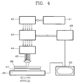
The above laser transcription method will now be
described in detail with reference to FIG. 4 schematically
showing a transcription apparatus used in a general laser
transcription method.
In FIG. 4, a high power laser beam is emitted from an
energy source 41. As the energy source emitting power at a
rate of 0.1~4W, a high power solid laser such as Nd/YAG, gas
laser such as CO2 and CO, or a diode-couple Nd/YAG can be
used. The emitted laser beam is divided into a plurality of
beams having the same intensity via a beam splitter 42. If
the intensity of the beam is controlled by dividing the beam
into a plurality of beams, a substance can be transcribed in
a desired shape (U.S. Patent No. 4,796,038).
The intensity of the plurality of divided laser beams
is controlled by a modulator 43 according to an intended
shape, and then the laser beam is irradiated on a donor film
46 on which the transcription substance is deposited, via a
condensing optical system 44. Here, only the substance
deposited on a light-receiving portion of the donor film is
transcribed onto a substrate 47. The movement of a stage 48
is controlled together with a raster 49 for controlling the
intensity of the bundle of the beam according to the shape
of the desired pattern.
The inventors of the present invention have conducted
research into a method for forming a flat-panel display
device of which a cell gap between upper and lower
substrates are uniformly maintained using the above-described
transcription method to thereby improve the
display characteristics of the flat-panel display device.
According to a first aspect of the present invention,
there is provided a liquid crystal display including first
and second substrates in which a transparent substrate, a
transparent electrode and an alignment layer are
sequentially stacked, and a liquid crystal layer of which
thickness is uniformly maintained by spacers formed between
the alignment layers of the first and second substrates,
wherein the height of each spacer and the interval between
two adjacent spacers are constant.
According to a second aspect of the present invention,
there is provided a method for manufacturing a liquid
crystal display, comprising the steps of: (a) forming first
and second substrates in which transparent substrates,
transparent electrodes and alignment layers are sequentially
stacked, respectively; (b) placing a donor film including a
base film, a light absorption layer and a transcription
layer in a position depart from the alignment layer of the
first substrate by a predetermined distance; (c)
transcribing the spacer forming polymer of the transcription
layer onto the first substrate by irradiating an energy
source toward the base film of the donor film to form
spacers, each spacer having equal height and the between two
adjacent spacers being uniform; (d) stacking the second
substrate on the first substrate on which spacers are
transcribed so as to face the alignment layers of two
substrates each other; and (e) sealing two substrates by
hardening the spacers by providing light or heat to at least
one of the first and second substrates to fix the spacers
between the alignment layers of the first and second
substrates.
According to a third aspect of the present invention,
there is provided a plasma display panel including a first
substrate in which a transparent substrate, an address
electrode and a dielectric layer are stacked in sequence, a
second substrate in which a transparent electrode, a bus
electrode and a dielectric layer are stacked in sequence,
and barrier walls formed between the first and second
substrates to separate the first and second substrates by a
predetermined distance, wherein each barrier wall has
uniform height and width.
According to a fourth aspect of the present invention,
there is provided a method for manufacturing a plasma
display panel comprising the steps of: (a) forming a first
substrate in which a transparent substrate, an address
electrode and a dielectric layer are stacked in sequence;
(b) forming a second substrate in which a transparent
substrate, a transparent electrode, a bus electrode and a
dielectric layer are stacked in sequence; (c) placing a
donor film including a base film, a light absorption layer
and a transcription layer in a position separated from the
dielectric layer of the first substrate by a predetermined
distance; (d) transcribing a barrier wall forming material
of the transcription layer on the first substrate by
irradiating a light source on the base film of the donor
film to form barrier walls, each barrier wall having uniform
height and width; (e) stacking the second substrate on the
first substrate so as to face the dielectric layers of two
substrates each other.
The present invention will now be described in detail
with reference to the accompanying drawings, in which:
FIG. 5 shows one embodiment of a liquid crystal display
(LCD) according to one aspect of the present invention. In
FIG. 5, reference numerals 51 and 51' represent first and
second substrates, reference numerals 52 and 52' represent
transparent substrates, reference numerals 53 and 53'
represent transparent electrodes, reference numerals 54 and
54' represent alignment layers, reference numeral 55
represents a spacer formed by transcription method, and
reference numeral 56 represents a liquid crystal layer,
respectively.
As can be seen from FIG. 5, the spacers having a
uniform height are formed at predetermined intervals.
The LCD shown in FIG. 5 is formed by the following
steps.
First, two transparent substrates 52 and 52' are
prepared, and the transparent electrodes 53 and 53' and the
alignment layers 54 and 54' are sequentially stacked on each
transparent substrate, to form the first and second
substrates 51 and 51'. Then, a donor film (not shown)
including a base film, a light absorption layer and a
transcription layer is positioned separated from the
alignment layer 54 of the first substrate 51 by a
predetermined interval. Then, a light source is irradiated
toward the base film of the donor film to transcribe a
spacer forming material of the transcription layer onto the
first substrate. Then, the second substrate 51' is stacked
on the first substrate 51 such that the alignment layers 54
and 54' of the first and second substrates 51 and 51' face
each other. Then, two substrates are sealed by applying
light or heat to one of the first and second substrates,
thereby completing a LCD.
FIG. 6 is a diagram illustrating the step of
transcribing the spacer forming material in detail.
First, a transparent substrate 67, a transparent
electrode 66, and an alignment layer 65 are sequentially
stacked to form a first substrate. Next, for transcription,
a light absorption layer 63 and a transcription layer 64 are
sequentially deposited on a base film 62 to manufacture a
donor film. Then, after facing the alignment layer 65
toward the transcription 64, a light source 61 is irradiated
toward the base film 62. The irradiated energy activates
the light absorption layer 63 via a laser transcription
device 60 and the base film 62, so that transcription energy
is emitted through the thermal decomposition reaction. By
the explosive force of the transcription energy, the spacer
forming material is transcribed onto the alignment layer.
As described above, the donor film has a structure in
which the base film, light absorption layer and
transcription layer are stacked in sequence.
In detail, preferably, the base film is formed of a
material having light transmittance of 90% or more, such as
polyethyleneterephthalate (PET) and polycarbonate.
The light absorption layer acts as a layer for
converting the received light into transcription energy, and
may include polymer or metal material.
The transcription layer includes a spacer forming
polymer as a main component, an initiator and a hardening
agent. Thus, two substrate can be sealed by hardening the
transcribed spacers by the following hardening step. That
is, an extra substrate sealing step using a sealant is not
necessary, so that the process is simplified. Here, the
polymer may be one selected from the group consisting of
polyacryl, polyimide, polyvinylalcohol (PVA),
polyvinylpyrrolidone (PVP), epoxy resin, phenol-formaldehyde
resin and an unsaturated polyester resin. Also, the
initiator may be an organic substance having an unstable
functional group such as azo (-N=N-), disulfide (-S-S-) and
peroxide (-O-O-) groups. In detail, benzol peroxide may be
used as an optical initiator, and benzophenon and imidazole
may be used as a thermal initiator. The hardening agent may
be anything which can be used in the field related with the
present invention.
On the other hand, a buffering layer may be further
included between the light absorption layer and the
transcription layer, which is for preventing the unevenness
of the transcription layer, caused by the energy transmitted
from the light absorption layer, and the partial
transcription of the transcription layer together with the
light absorption layer.
Also, as a light source which can be used to transcribe
the transcription layer, UV/VIS light source such as a laser
beam, xenon lamp or halogen lamp, or a thermal head may be
used. The substrate may be sealed by hardening the spacers
by providing light or heat energy from a proper light
source. Here, the light or heat energy source used for
hardening the spacers may be the same as that used for the
transcription, preferably, a high-pressure mercury lamp, a
xenon lamp or a flash lamp.
In the LCD manufactured by the above-described
manufacturing method, preferably, the height of each spacer
is 0.5~10µm, and the interval between adjacent two spacers
is 10~1,000µm.
On the other hand, a color LCD may be manufactured by
further forming a color filter layer consisting of color
filters (red, green and blue filters) on one of two
substrates. If required, a protective film may be further
formed on the color filter layer.
In this case, the spacers are formed in the liquid
crystal layer corresponding to each portion between every
adjacent two color filters, i.e., a portion in which black
matrixes are to be formed, in a size so as to cover the
portion between adjacent two color filters. Also, each
spacer has an absorbency of 2 or more and a height of
0.5~10µm.
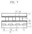
An LCD having the above structure is shown in FIG. 7.
In FIG. 7, reference numerals 71 and 71' represent
transparent substrates, reference numeral 72 represents
color filter layer, reference numerals 73, 74 and 75
represent red, green and blue color filters, respectively,
reference numeral 76 represents protective film, reference
numerals 77 and 77' represent transparent electrodes,
reference numerals 78 and 78' represent alignment layers,
and reference numerals 79 represent opaque spacers formed at
positions where black matrixes are to be formed,
respectively.
As can be seen from FIG. 7, the opaque spacers are
formed in the positions where the black matrixes are to be
formed such that the opaque spacers act as a black matrix as
well as a spacer. Thus, there is no need to form extra
black matrixes. Also, the height of each opaque spacers
formed by the above method is 0.5~10µm which is greater than
that (about 1,400Å) of the conventional black matrix, so
that the enhanced effect for preventing mixing of colors and
improving the high-luminance characteristic can be achieved.
A plasma display panel (PDP) of the present invention
is manufactured by the following method:
First, two transparent substrates are prepared. An
address electrode and a dielectric layer are sequentially
formed on the one of the transparent substrates, and a
transparent electrode, a bus electrode and a dielectric
layer are sequentially formed on the other transparent
substrate, thereby resulting in first and second substrates.
Then, a donor film including a base film, a light absorption
layer and a transcription layer is positioned separated from
the dielectric layer of the first substrate by a
predetermined distance. Then, a light source is irradiated
on the donor film to transcribe a barrier wall forming
material onto the first substrate, and the second substrate
is then stacked on the first substrate such that the
dielectric layers of the first and second substrates face
each other, thereby completing the PDP.
In the above manufacturing method for the PDP of the
present invention, the donor film has a structure in which
the base film, light absorption layer and transcription
layer are stacked in sequence.
In detail, the base film and light absorption layer are
the same as those described in the manufacturing method for
the LCD, and the transcription layer may include a barrier
wall forming material, such as alumina (Al2O3) or glass
powder.
Also, as described above, a buffering layer may be
further included between the light absorption layer and the
transcription layer.
On the other hand, the light source used for the
transcription is the same as that described in the
manufacturing method for the LCD.
Also, the manufacturing method for the PDP may further
include the step of forming multilayered barrier walls by
repeating the transcription steps several times before the
second substrate is stacked on the first substrate. As a
result, barrier walls having the intended height can be
obtained.
In the PDP obtained by the above steps, preferably, the
height and width of each barrier wall are 10~several
hundreds µm and 20~300µm, respectively.
The present invention provides the following
advantages.
First, in the LCD, the spacer forming material having
a predetermined height is transcribed on an intended
position, so that the spacers do not agglomerate as in the
conventional spacer deposition method, resulting in a cell
gap of even interval. Also, two substrates are sealed by
hardening the transcribed spacers, so that an additional
substrate sealing process is not required. Also, there is
no damage to the electrode by the spacers, occurring during
the conventional substrate sealing process under heat and
pressure. Also, the spacer forming material is hardened by
light (or heat) and then fixed between two substrates, so
that the damage to the alignment layer during the injection
of liquid crystals, caused by the flowing of spacers, can be
prevented.
In the case of the color LCD, opaque spacers function
as a light shelter like the conventional black matrix as
well. Thus, an additional black matrix forming process is
not required.
That is, in the manufacturing method for the LCD
according to the present invention, mixing of colors between
pixels is prevented, providing high luminance
characteristics through a simple manufacturing process.
As described above, the LCD and the manufacturing
method therefor according to the present invention can be
applied to manufacture FLCD, STN-LCD, TFT-LCD, TN-LCD and
plastic LCD.
In addition, in the case of the PDP, each barrier wall
having uniform height and width are formed, the electrical
and optical blocking effect between adjacent cells, and
resolution are remarkably enhanced, thereby improving
display quality of an image. Also, the manufacturing method
for the PDP is simpler than the conventional method, and
inferiority ratio is also low.