EP0825639A2 - Silicon wafer and method of manufacturing the same - Google Patents

Silicon wafer and method of manufacturing the same Download PDF

Info

Publication number
EP0825639A2
EP0825639A2 EP97306225A EP97306225A EP0825639A2 EP 0825639 A2 EP0825639 A2 EP 0825639A2 EP 97306225 A EP97306225 A EP 97306225A EP 97306225 A EP97306225 A EP 97306225A EP 0825639 A2 EP0825639 A2 EP 0825639A2
Authority
EP
European Patent Office
Prior art keywords
silicon wafer
film
silicon
cvd film
layer
Prior art date
Legal status (The legal status is an assumption and is not a legal conclusion. Google has not performed a legal analysis and makes no representation as to the accuracy of the status listed.)
Withdrawn
Application number
EP97306225A
Other languages
German (de)
French (fr)
Other versions
EP0825639A3 (en
Inventor
Shoichi Takamizawa
Norihiro Kobayashi
Current Assignee (The listed assignees may be inaccurate. Google has not performed a legal analysis and makes no representation or warranty as to the accuracy of the list.)
Shin Etsu Handotai Co Ltd
Original Assignee
Shin Etsu Handotai Co Ltd
Priority date (The priority date is an assumption and is not a legal conclusion. Google has not performed a legal analysis and makes no representation as to the accuracy of the date listed.)
Filing date
Publication date
Application filed by Shin Etsu Handotai Co Ltd filed Critical Shin Etsu Handotai Co Ltd
Publication of EP0825639A2 publication Critical patent/EP0825639A2/en
Publication of EP0825639A3 publication Critical patent/EP0825639A3/en
Withdrawn legal-status Critical Current

Links

Images

Classifications

    • HELECTRICITY
    • H01ELECTRIC ELEMENTS
    • H01LSEMICONDUCTOR DEVICES NOT COVERED BY CLASS H10
    • H01L21/00Processes or apparatus adapted for the manufacture or treatment of semiconductor or solid state devices or of parts thereof
    • H01L21/02Manufacture or treatment of semiconductor devices or of parts thereof
    • H01L21/02104Forming layers
    • H01L21/02107Forming insulating materials on a substrate
    • H01L21/02225Forming insulating materials on a substrate characterised by the process for the formation of the insulating layer
    • H01L21/0226Forming insulating materials on a substrate characterised by the process for the formation of the insulating layer formation by a deposition process
    • H01L21/02263Forming insulating materials on a substrate characterised by the process for the formation of the insulating layer formation by a deposition process deposition from the gas or vapour phase
    • H01L21/02271Forming insulating materials on a substrate characterised by the process for the formation of the insulating layer formation by a deposition process deposition from the gas or vapour phase deposition by decomposition or reaction of gaseous or vapour phase compounds, i.e. chemical vapour deposition
    • H01L21/02274Forming insulating materials on a substrate characterised by the process for the formation of the insulating layer formation by a deposition process deposition from the gas or vapour phase deposition by decomposition or reaction of gaseous or vapour phase compounds, i.e. chemical vapour deposition in the presence of a plasma [PECVD]
    • HELECTRICITY
    • H01ELECTRIC ELEMENTS
    • H01LSEMICONDUCTOR DEVICES NOT COVERED BY CLASS H10
    • H01L21/00Processes or apparatus adapted for the manufacture or treatment of semiconductor or solid state devices or of parts thereof
    • H01L21/02Manufacture or treatment of semiconductor devices or of parts thereof
    • H01L21/02104Forming layers
    • H01L21/02107Forming insulating materials on a substrate
    • H01L21/02109Forming insulating materials on a substrate characterised by the type of layer, e.g. type of material, porous/non-porous, pre-cursors, mixtures or laminates
    • H01L21/02112Forming insulating materials on a substrate characterised by the type of layer, e.g. type of material, porous/non-porous, pre-cursors, mixtures or laminates characterised by the material of the layer
    • H01L21/02123Forming insulating materials on a substrate characterised by the type of layer, e.g. type of material, porous/non-porous, pre-cursors, mixtures or laminates characterised by the material of the layer the material containing silicon
    • H01L21/02126Forming insulating materials on a substrate characterised by the type of layer, e.g. type of material, porous/non-porous, pre-cursors, mixtures or laminates characterised by the material of the layer the material containing silicon the material containing Si, O, and at least one of H, N, C, F, or other non-metal elements, e.g. SiOC, SiOC:H or SiONC
    • H01L21/0214Forming insulating materials on a substrate characterised by the type of layer, e.g. type of material, porous/non-porous, pre-cursors, mixtures or laminates characterised by the material of the layer the material containing silicon the material containing Si, O, and at least one of H, N, C, F, or other non-metal elements, e.g. SiOC, SiOC:H or SiONC the material being a silicon oxynitride, e.g. SiON or SiON:H
    • HELECTRICITY
    • H01ELECTRIC ELEMENTS
    • H01LSEMICONDUCTOR DEVICES NOT COVERED BY CLASS H10
    • H01L21/00Processes or apparatus adapted for the manufacture or treatment of semiconductor or solid state devices or of parts thereof
    • H01L21/02Manufacture or treatment of semiconductor devices or of parts thereof
    • H01L21/02104Forming layers
    • H01L21/02107Forming insulating materials on a substrate
    • H01L21/02109Forming insulating materials on a substrate characterised by the type of layer, e.g. type of material, porous/non-porous, pre-cursors, mixtures or laminates
    • H01L21/02112Forming insulating materials on a substrate characterised by the type of layer, e.g. type of material, porous/non-porous, pre-cursors, mixtures or laminates characterised by the material of the layer
    • H01L21/02123Forming insulating materials on a substrate characterised by the type of layer, e.g. type of material, porous/non-porous, pre-cursors, mixtures or laminates characterised by the material of the layer the material containing silicon
    • H01L21/02164Forming insulating materials on a substrate characterised by the type of layer, e.g. type of material, porous/non-porous, pre-cursors, mixtures or laminates characterised by the material of the layer the material containing silicon the material being a silicon oxide, e.g. SiO2
    • HELECTRICITY
    • H01ELECTRIC ELEMENTS
    • H01LSEMICONDUCTOR DEVICES NOT COVERED BY CLASS H10
    • H01L21/00Processes or apparatus adapted for the manufacture or treatment of semiconductor or solid state devices or of parts thereof
    • H01L21/02Manufacture or treatment of semiconductor devices or of parts thereof
    • H01L21/02104Forming layers
    • H01L21/02107Forming insulating materials on a substrate
    • H01L21/02109Forming insulating materials on a substrate characterised by the type of layer, e.g. type of material, porous/non-porous, pre-cursors, mixtures or laminates
    • H01L21/02112Forming insulating materials on a substrate characterised by the type of layer, e.g. type of material, porous/non-porous, pre-cursors, mixtures or laminates characterised by the material of the layer
    • H01L21/02123Forming insulating materials on a substrate characterised by the type of layer, e.g. type of material, porous/non-porous, pre-cursors, mixtures or laminates characterised by the material of the layer the material containing silicon
    • H01L21/0217Forming insulating materials on a substrate characterised by the type of layer, e.g. type of material, porous/non-porous, pre-cursors, mixtures or laminates characterised by the material of the layer the material containing silicon the material being a silicon nitride not containing oxygen, e.g. SixNy or SixByNz
    • HELECTRICITY
    • H01ELECTRIC ELEMENTS
    • H01LSEMICONDUCTOR DEVICES NOT COVERED BY CLASS H10
    • H01L21/00Processes or apparatus adapted for the manufacture or treatment of semiconductor or solid state devices or of parts thereof
    • H01L21/02Manufacture or treatment of semiconductor devices or of parts thereof
    • H01L21/04Manufacture or treatment of semiconductor devices or of parts thereof the devices having at least one potential-jump barrier or surface barrier, e.g. PN junction, depletion layer or carrier concentration layer
    • H01L21/18Manufacture or treatment of semiconductor devices or of parts thereof the devices having at least one potential-jump barrier or surface barrier, e.g. PN junction, depletion layer or carrier concentration layer the devices having semiconductor bodies comprising elements of Group IV of the Periodic System or AIIIBV compounds with or without impurities, e.g. doping materials
    • H01L21/22Diffusion of impurity materials, e.g. doping materials, electrode materials, into or out of a semiconductor body, or between semiconductor regions; Interactions between two or more impurities; Redistribution of impurities
    • H01L21/2205Diffusion of impurity materials, e.g. doping materials, electrode materials, into or out of a semiconductor body, or between semiconductor regions; Interactions between two or more impurities; Redistribution of impurities from the substrate during epitaxy, e.g. autodoping; Preventing or using autodoping
    • HELECTRICITY
    • H01ELECTRIC ELEMENTS
    • H01LSEMICONDUCTOR DEVICES NOT COVERED BY CLASS H10
    • H01L21/00Processes or apparatus adapted for the manufacture or treatment of semiconductor or solid state devices or of parts thereof
    • H01L21/02Manufacture or treatment of semiconductor devices or of parts thereof
    • H01L21/04Manufacture or treatment of semiconductor devices or of parts thereof the devices having at least one potential-jump barrier or surface barrier, e.g. PN junction, depletion layer or carrier concentration layer
    • H01L21/18Manufacture or treatment of semiconductor devices or of parts thereof the devices having at least one potential-jump barrier or surface barrier, e.g. PN junction, depletion layer or carrier concentration layer the devices having semiconductor bodies comprising elements of Group IV of the Periodic System or AIIIBV compounds with or without impurities, e.g. doping materials
    • H01L21/30Treatment of semiconductor bodies using processes or apparatus not provided for in groups H01L21/20 - H01L21/26
    • H01L21/31Treatment of semiconductor bodies using processes or apparatus not provided for in groups H01L21/20 - H01L21/26 to form insulating layers thereon, e.g. for masking or by using photolithographic techniques; After treatment of these layers; Selection of materials for these layers
    • H01L21/314Inorganic layers
    • H01L21/3143Inorganic layers composed of alternated layers or of mixtures of nitrides and oxides or of oxinitrides, e.g. formation of oxinitride by oxidation of nitride layers
    • H01L21/3145Inorganic layers composed of alternated layers or of mixtures of nitrides and oxides or of oxinitrides, e.g. formation of oxinitride by oxidation of nitride layers formed by deposition from a gas or vapour
    • HELECTRICITY
    • H01ELECTRIC ELEMENTS
    • H01LSEMICONDUCTOR DEVICES NOT COVERED BY CLASS H10
    • H01L21/00Processes or apparatus adapted for the manufacture or treatment of semiconductor or solid state devices or of parts thereof
    • H01L21/02Manufacture or treatment of semiconductor devices or of parts thereof
    • H01L21/04Manufacture or treatment of semiconductor devices or of parts thereof the devices having at least one potential-jump barrier or surface barrier, e.g. PN junction, depletion layer or carrier concentration layer
    • H01L21/18Manufacture or treatment of semiconductor devices or of parts thereof the devices having at least one potential-jump barrier or surface barrier, e.g. PN junction, depletion layer or carrier concentration layer the devices having semiconductor bodies comprising elements of Group IV of the Periodic System or AIIIBV compounds with or without impurities, e.g. doping materials
    • H01L21/30Treatment of semiconductor bodies using processes or apparatus not provided for in groups H01L21/20 - H01L21/26
    • H01L21/322Treatment of semiconductor bodies using processes or apparatus not provided for in groups H01L21/20 - H01L21/26 to modify their internal properties, e.g. to produce internal imperfections
    • H01L21/3221Treatment of semiconductor bodies using processes or apparatus not provided for in groups H01L21/20 - H01L21/26 to modify their internal properties, e.g. to produce internal imperfections of silicon bodies, e.g. for gettering
    • HELECTRICITY
    • H01ELECTRIC ELEMENTS
    • H01LSEMICONDUCTOR DEVICES NOT COVERED BY CLASS H10
    • H01L21/00Processes or apparatus adapted for the manufacture or treatment of semiconductor or solid state devices or of parts thereof
    • H01L21/02Manufacture or treatment of semiconductor devices or of parts thereof
    • H01L21/02104Forming layers
    • H01L21/02107Forming insulating materials on a substrate
    • H01L21/02109Forming insulating materials on a substrate characterised by the type of layer, e.g. type of material, porous/non-porous, pre-cursors, mixtures or laminates
    • H01L21/02205Forming insulating materials on a substrate characterised by the type of layer, e.g. type of material, porous/non-porous, pre-cursors, mixtures or laminates the layer being characterised by the precursor material for deposition
    • H01L21/02208Forming insulating materials on a substrate characterised by the type of layer, e.g. type of material, porous/non-porous, pre-cursors, mixtures or laminates the layer being characterised by the precursor material for deposition the precursor containing a compound comprising Si
    • H01L21/02211Forming insulating materials on a substrate characterised by the type of layer, e.g. type of material, porous/non-porous, pre-cursors, mixtures or laminates the layer being characterised by the precursor material for deposition the precursor containing a compound comprising Si the compound being a silane, e.g. disilane, methylsilane or chlorosilane
    • YGENERAL TAGGING OF NEW TECHNOLOGICAL DEVELOPMENTS; GENERAL TAGGING OF CROSS-SECTIONAL TECHNOLOGIES SPANNING OVER SEVERAL SECTIONS OF THE IPC; TECHNICAL SUBJECTS COVERED BY FORMER USPC CROSS-REFERENCE ART COLLECTIONS [XRACs] AND DIGESTS
    • Y10TECHNICAL SUBJECTS COVERED BY FORMER USPC
    • Y10STECHNICAL SUBJECTS COVERED BY FORMER USPC CROSS-REFERENCE ART COLLECTIONS [XRACs] AND DIGESTS
    • Y10S148/00Metal treatment
    • Y10S148/024Defect control-gettering and annealing
    • YGENERAL TAGGING OF NEW TECHNOLOGICAL DEVELOPMENTS; GENERAL TAGGING OF CROSS-SECTIONAL TECHNOLOGIES SPANNING OVER SEVERAL SECTIONS OF THE IPC; TECHNICAL SUBJECTS COVERED BY FORMER USPC CROSS-REFERENCE ART COLLECTIONS [XRACs] AND DIGESTS
    • Y10TECHNICAL SUBJECTS COVERED BY FORMER USPC
    • Y10STECHNICAL SUBJECTS COVERED BY FORMER USPC CROSS-REFERENCE ART COLLECTIONS [XRACs] AND DIGESTS
    • Y10S148/00Metal treatment
    • Y10S148/06Gettering

Definitions

  • the present invention relates to a silicon wafer and a method of manufacturing the silicon wafer, and more particularly a silicon wafer which has a film formed by chemical vapor deposition (a CVD film), particularly a film formed by plasma chemical vapor deposition (a plasma CVD film), serving as both a gettering layer and a protective film for preventing autodoping. Further, the present invention relates to a silicon epitaxial wafer produced from the silicon wafer.
  • a CVD film chemical vapor deposition
  • a plasma CVD film plasma chemical vapor deposition
  • a device is fabricated on one main face (hereinafter referred to as a "front surface") of the silicon wafer.
  • the technique of forming a thin film on the other main face (hereinafter referred to as a "back surface") of the silicon wafer has two principal objects.
  • One object is to utilize the thin film as a layer for gettering impurities such as heavy metals, and the other object is to utilize the thin film as a protective film for preventing autodoping that would otherwise occur when a layer is epitaxially grown on the silicon wafer.
  • Gettering is the technique of collecting impurities, such as heavy metals, produced during the course of manufacture of a silicon electronic device on the silicon wafer outside the regions in the vicinity of the front surface of the silicon wafer where devices are fabricated.
  • impurities such as heavy metals
  • one representative gettering technique is the technique of forming a gettering layer by depositing polycrystalline silicon on the back surface of the silicon wafer through use of low-pressure chemical vapor deposition (the low-pressure CVD method).
  • the low-pressure CVD method low-pressure chemical vapor deposition
  • a method of depositing amorphous silicon in place of the polycrystalline silicon see Japanese Patent Application Laid-open No. 4-2133.
  • Autodoping is a phenomenon in which a dopant evaporates principally from the back surface of the silicon wafer into the gas phase to be used for epitaxial growth when a silicon epitaxial wafer is manufactured, and the thus-evaporated dopant is incorporated into the epitaxial layer.
  • a transition width i.e., the width of an area where the concentration of dopants changes in the vicinity of the interface between an epitaxial layer and the silicon wafer
  • the device fails to exhibit its originally-designed characteristics, thereby rendering the device defective.
  • a protective film for the purpose of preventing autodoping is formed on the back surface of a silicon wafer in order to prevent the autodoping in a case where the silicon wafer having a high concentration of dopants is subjected to epitaxial growth.
  • An atmospheric-pressure silicon oxide film (an atmospheric-pressure CVD oxide film) grown in an atmospheric-pressure chemical vapor deposition apparatus (an atmospheric-pressure CVD system) is primarily used as the protective film.
  • the gettering layer is formed by depositing the polycrystalline silicon or amorphous silicon, there are only a limited number of elements which can be expected to be removed by gettering. For this reason, there is a limit to the gettering capability of the gettering layer.
  • the silicon wafer receives heat during the fabrication of the device, transformation of the polycrystalline silicon or amorphous silicon into monocrystalline silicon proceeds, thereby resulting in deterioration of the gettering capability.
  • a silicon monocrystal is epitaxially grown on the front surface of the silicon wafer having a gettering layer of polycrystalline or amorphous silicon on the back surface
  • dopants easily penetrate through the polycrystalline or amorphous silicon.
  • the silicon wafer to be subjected to epitaxial growth contains a high concentration of dopants
  • polycrystalline or amorphous silicon is deposited on the back surface of the silicon wafer, and an atmospheric-pressure CVD oxide film is further deposited on the polycrystalline or amorphous silicon, thereby preventing autodoping.
  • an object of the present invention is to provide a silicon wafer having a thin film provided on the back surface, which thin film has an excellent and persistent gettering capability that can remove a greater variety of types of elements, and can prevent autodoping.
  • the present inventors have discovered that this object can be accomplished by formation of a CVD film whose components and/or composition change in the thicknesswise direction of the film through use of the chemical vapor deposition (CVD) method.
  • the CVD method by the CVD method, the CVD film whose components and/or composition change in the thicknesswise direction of the film can be formed through one process step or in a consecutive manner. Consequently, a CVD film consisting of many types of layers of differing components, or a CVD film whose composition continuously changes in the thicknesswise direction of the film can be inexpensively formed.
  • Such a CVD film whose components and/or composition change in the thicknesswise direction of the film can remove a greater variety of types of elements in comparison with the conventional CVD film, and has improved persistent gettering capability. Further, the CVD film can prevent autodoping.
  • the CVD film whose components and/or composition change in the thicknesswise direction of the film possesses high gettering capability even if the thickness of the film is comparatively small.
  • a silicon wafer having a CVD film formed on one main face (the back surface) and having the other main face mirror-polished (the front surface), wherein the components and/or composition of the CVD film change in the thicknesswise direction of the film.
  • the components and/or composition of the CVD film change within any one of the ranges 0 ⁇ suffix x ⁇ 2 for SiO x , 0 ⁇ suffix z ⁇ 1.34 for SiN z , or 0 ⁇ suffix x ⁇ 2, 0 ⁇ suffix y ⁇ 1.34 for SiO x N y . If the components and/or composition of the CVD film change within this range, the gettering capability and the autodoping prevention capability of the silicon wafer become superior. Further, with these conditions, it is easy to obtain materials to be used for formation of such a CVD film.
  • the components and/or composition of the CVD film changes in the thicknesswise direction of the film within the range of 0 ⁇ suffix x ⁇ 2 for SiO x .
  • a CVD film is realized by comprising: e.g.,
  • the CVD film comprising the amorphous silicon layer and the SiO x layer whose composition changes [corresponding to iii)] and the CVD film comprising the amorphous silicon layer, the SiN y layer whose composition changes, and one SiO x layer [corresponding to v]] are particularly preferable.
  • These CVD films are capable of removing a greater variety of types of elements by gettering and possess particularly superior gettering capability. Further, in these CVD films, it takes considerably long for the amorphous silicon layer to become monocrystalline, and therefore the CVD films are particularly superior in terms of persistency of the gettering capability.
  • a layer which contains O or N in as high proportions as possible should preferably be provided as the outermost stacked layer of the CVD film in order to ensure prevention of the autodoping effect.
  • a plasma CVD film formed by plasma CVD is particularly preferable.
  • the reason for this is that the plasma CVD permits comparatively easy manufacture of a plasma CVD film only in one process step.
  • a method of manufacturing the foregoing silicon wafer wherein a CVD film is formed on one main face of the silicon wafer in one process step or in a consecutive manner by CVD in such a way that the components and/or composition of the CVD film change in the thicknesswise direction of the film.
  • the CVD film whose components and/or composition change in the thicknesswise direction of the film can be formed in a single process step or in a consecutive manner.
  • the CVD film in such a way that the components and/or composition of the film change in the thicknesswise direction, there is obtained a silicon wafer which has an excellent and persistent superior gettering capability and prevents the autodoping effect.
  • a common silicon-wafer manufacturing method comprises the steps of: slicing a silicon monocrystal rod into silicon wafers; and chamfering, lapping, chemical etching, and mirror-polishing the thus-obtained wafers.
  • the CVD film is formed after the wafer has been subjected to chemical etching or after one side or both sides of the wafer have been mirror-polished.
  • the CVD film is formed on the back surface of the wafer so as to be prevented from going around to the main face. As a result, a step to mirror-polish the main face can be omitted.
  • the CVD film can be formed in one process step or in a consecutive manner such that the components and/or composition of the film change in its thicknesswise direction by changing conditions for growing the CVD film, such as a deposition temperature, a deposition pressure, the type of reaction gas, and the flow rate of the gas, in accordance with the application of the silicon wafer.
  • the silicon wafer is a silicon epitaxial wafer in which a silicon monocrystalline thin-film is epitaxially grown on the mirror-polished main face of the silicon wafer.
  • a transition area is narrow, and the resistivity of the epitaxial layer is controlled superiorly.
  • a silicon device fabricated through use of such a silicon epitaxial wafer exhibits the characteristics as designed.
  • the present invention makes it possible to inexpensively provide a silicon wafer having an excellent and persistent gettering layer which has gettering capability with respect to a greater variety of types of elements and autodoping-prevention capability. Further, an epitaxial wafer having a narrow transition width can be provided as a result of use of such a silicon wafer.
  • a silicon wafer 1 is first prepared by a known manufacturing method (FIG. 1A).
  • a chemically-etched wafer before it is mirror-polished is commonly used as this silicon wafer 1
  • a mirror-polished wafer which is mirror-polished at one or both sides may be also employed.
  • a CVD film 2 is deposited on the back surface of the silicon wafer through use of a CVD apparatus (FIG. 1B).
  • the components and composition of a CVD film to be deposited are changed in the thicknesswise direction of the film.
  • component x, y, or z in one film is changed in the thicknesswise direction of the CVD film.
  • Such a CVD film is provided with superior gettering and autodoping-prevention capability, and source gases of such a CVD film are easy to obtain.
  • the components and composition of the CVD film can be changed in the thicknesswise direction of a CVD film to be deposited by programming the CVD apparatus with regard to the deposition temperature, the deposition pressure, the deposition time, the type of reactive gas, or the flow rate in accordance with the application of the silicon wafer. Accordingly, the CVD film whose components and composition change in the thicknesswise direction thereof can be deposited on a silicon wafer in one process step or in a consecutive manner. In this event, the thickness of a CVD film to be deposited is preferably within the range of 50 to 500 nm. Further, the deposition temperature and pressure are preferably within the range of 100 to 450 °C and 0.1 to 10 torr, respectively.
  • the front surface and the edge of the silicon wafer are mirror-polished (FIG. 1C).
  • the CVD film deposited on the front surface of the silicon wafer to be mirror-polished can be finished at a very high speed, whereby the CVD film can be easily removed without impairing the flatness of the silicon wafer by polishing.
  • a CVD film is deposited on the back surface of the silicon wafer so as not to pass around to the mirror-polished surface, whereby a step to mirror polish the front surface after the deposition of the CVD film can be omitted.
  • a silicon monocrystalline rod produced by the Czochralski method [the silicon monocrystal has a (100) main face, a p-type conductivity, and a resistivity of 0.01 ⁇ ⁇ cm] was sliced to obtain four wafers (CZ wafers), which were then subjected to chamfering, lapping, and chemical etching processes.
  • a silicon monocrystalline rod produced by the floating zone method [the silicon monocrystal has a (100) main face, an n-type conductivity, and a resistivity of 20 ⁇ ⁇ cm] was sliced to obtain eight wafers (FZ wafers), which were then subjected to chamfering, lapping, and chemical etching processes.
  • a plasma CVD film which was comprised of a component Si and O and was grown through use of a plasma CVD apparatus: Growth Conditions:
  • a plasma CVD film which was comprised of components Si, O, N and was grown through use of the plasma CVD apparatus: Growth Conditions:
  • a polycrystalline silicon film grown through use of a low-pressure CVD apparatus Growth Conditions:
  • a solution containing a plurality of heavy metal ions (iron, copper, chrome, and nickel ions) was applied to each front surface of the four types of wafers, so that the wafers were intentionally contaminated. Subsequently, they undergone heat treatment at 1000 °C for 1 hr, whereby the heavy metal ions were diffused into the wafer. Subsequently, after they had been subjected to heat treatment at 650 °C for 10 hrs., the concentration of heavy metals in each silicon wafer with the exception of its gettering layer was measured through use of the DLTS method (Deep Level Transient Spectroscopy) and the ICP-MS method (Inductively-coupled Plasma Mass Spectrometer). While the concentration of each heavy metal contained in the wafer without the gettering layer was used as a standard, the proportion of each heavy metal captured in each gettering layer was calculated from the resultant measurement of the concentration of each heavy metal.
  • the concentration of each heavy metal contained in the wafer without the gettering layer was
  • Table 2 shows the results of such calculation. Capability of gettering various heavy metals Iron Copper Chromium Nickel Example 1 99% 89% 85% 75% Example 2 99% 87% 85% 77% Comparative example 1 93% 72% 35% 25% Comparative example 2 0% 0% 0% 0% 0%
  • Table 2 shows that the plasma CVD film in accordance with the present invention exhibits a sufficient gettering effect with respect to chromium and nickel in comparison with the polycrystalline silicon film of the comparative example 1 which exhibits an insufficient gettering effect. Accordingly, it is acknowledged that the plasma CVD film in accordance with the present invention possesses superior gettering capability than that of the polycrystalline silicon film.
  • Table 3 shows the results of such calculation. Gettering capability Example 1 90% Example 2 90% Comparative example 1 70% Comparative example 2 0%
  • Table 3 shows that the plasma CVD film in accordance with the present invention retains superior gettering capability after having undergone heat treatment in comparison with the polycrystalline silicon film of Comparative example 1; namely, the plasma CVD film is superior in the persistency of gettering capability.
  • An epitaxial layer was grown on each of the four types of wafers under the following conditions through use of an epitaxial growth apparatus.
  • Example 1 Example 2 Comparative example 1 Comparative example 2 Transition width 1.4 ⁇ m 1.4 ⁇ m 1.6 ⁇ m 2.5 ⁇ m
  • Table 4 shows that the silicon wafer having the plasma CVD film in accordance with the present invention has a narrower transition width than that of the silicon wafer having the polycrystalline silicon film. It is acknowledged that the plasma CVD film in accordance with the present invention has superior autodoping-prevention capability at the time of epitaxial growth as well as superior gettering capability.

Abstract

In a silicon wafer having a CVD film formed on one main face and having the other main face mirror-polished, the components and/or composition of the CVD film change in the thicknesswise direction of the film. This makes it possible to provide a silicon wafer having a thin film provided on the back surface, which thin film has excellent and persistent gettering capability that can remove a greater variety of types of elements and can prevent autodoping.

Description

BACKGROUND OF THE INVENTION Field of the Invention:
The present invention relates to a silicon wafer and a method of manufacturing the silicon wafer, and more particularly a silicon wafer which has a film formed by chemical vapor deposition (a CVD film), particularly a film formed by plasma chemical vapor deposition (a plasma CVD film), serving as both a gettering layer and a protective film for preventing autodoping. Further, the present invention relates to a silicon epitaxial wafer produced from the silicon wafer.
Description of the Related Art:
Of the two main faces of a silicon wafer other than its edge, a device is fabricated on one main face (hereinafter referred to as a "front surface") of the silicon wafer. The technique of forming a thin film on the other main face (hereinafter referred to as a "back surface") of the silicon wafer has two principal objects.
One object is to utilize the thin film as a layer for gettering impurities such as heavy metals, and the other object is to utilize the thin film as a protective film for preventing autodoping that would otherwise occur when a layer is epitaxially grown on the silicon wafer.
Gettering is the technique of collecting impurities, such as heavy metals, produced during the course of manufacture of a silicon electronic device on the silicon wafer outside the regions in the vicinity of the front surface of the silicon wafer where devices are fabricated. By virtue of this technique, there can be prevented the degradation of the characteristics of the devices by impurities such as heavy metals, which in turn allows an increase in the ratio of non-defective silicon devices to the entire silicon devices to be manufactured.
As disclosed in, e.g., Japanese Patent Application Laid-open No. 59-186331, one representative gettering technique is the technique of forming a gettering layer by depositing polycrystalline silicon on the back surface of the silicon wafer through use of low-pressure chemical vapor deposition (the low-pressure CVD method). In order to improve the gettering capability, there has been proposed a method of depositing amorphous silicon in place of the polycrystalline silicon (see Japanese Patent Application Laid-open No. 4-2133).
Autodoping is a phenomenon in which a dopant evaporates principally from the back surface of the silicon wafer into the gas phase to be used for epitaxial growth when a silicon epitaxial wafer is manufactured, and the thus-evaporated dopant is incorporated into the epitaxial layer.
In a case where the resistivity of the silicon wafer to be subjected to epitaxial growth is low, or where there is a high concentration of dopants, autodoping occurs to a noticeable extent. If the epitaxial layer containing dopants in small concentration is grown, a transition width (i.e., the width of an area where the concentration of dopants changes in the vicinity of the interface between an epitaxial layer and the silicon wafer) is extended, which makes it difficult to control the resistivity of the epitaxial layer. If a silicon device is fabricated through use of a silicon wafer having an epitaxial layer with a wide transition area, the device fails to exhibit its originally-designed characteristics, thereby rendering the device defective.
For this reason, in a commonly-used technique, a protective film for the purpose of preventing autodoping is formed on the back surface of a silicon wafer in order to prevent the autodoping in a case where the silicon wafer having a high concentration of dopants is subjected to epitaxial growth. An atmospheric-pressure silicon oxide film (an atmospheric-pressure CVD oxide film) grown in an atmospheric-pressure chemical vapor deposition apparatus (an atmospheric-pressure CVD system) is primarily used as the protective film.
As the integration and performance of the silicon device have been improving in recent years, there has arisen a demand for improvements in persistency of gettering capability of the silicon wafer to be used as a material of the silicon electronic device, in addition to a demand for improvements in the gettering capability.
However, if the gettering layer is formed by depositing the polycrystalline silicon or amorphous silicon, there are only a limited number of elements which can be expected to be removed by gettering. For this reason, there is a limit to the gettering capability of the gettering layer. As the silicon wafer receives heat during the fabrication of the device, transformation of the polycrystalline silicon or amorphous silicon into monocrystalline silicon proceeds, thereby resulting in deterioration of the gettering capability. Thus, there is a problem with the persistency of the gettering capability of the silicon wafer.
In a case where a silicon monocrystal is epitaxially grown on the front surface of the silicon wafer having a gettering layer of polycrystalline or amorphous silicon on the back surface, dopants easily penetrate through the polycrystalline or amorphous silicon. Particularly, in a case where the silicon wafer to be subjected to epitaxial growth contains a high concentration of dopants, polycrystalline or amorphous silicon is deposited on the back surface of the silicon wafer, and an atmospheric-pressure CVD oxide film is further deposited on the polycrystalline or amorphous silicon, thereby preventing autodoping. These deposition operations are carried out in individual steps, so that the production cost increases.
SUMMARY OF THE INVENTION
In view of the foregoing descriptions, an object of the present invention is to provide a silicon wafer having a thin film provided on the back surface, which thin film has an excellent and persistent gettering capability that can remove a greater variety of types of elements, and can prevent autodoping.
The present inventors have discovered that this object can be accomplished by formation of a CVD film whose components and/or composition change in the thicknesswise direction of the film through use of the chemical vapor deposition (CVD) method. In other words, by the CVD method, the CVD film whose components and/or composition change in the thicknesswise direction of the film can be formed through one process step or in a consecutive manner. Consequently, a CVD film consisting of many types of layers of differing components, or a CVD film whose composition continuously changes in the thicknesswise direction of the film can be inexpensively formed. Such a CVD film whose components and/or composition change in the thicknesswise direction of the film can remove a greater variety of types of elements in comparison with the conventional CVD film, and has improved persistent gettering capability. Further, the CVD film can prevent autodoping. Moreover, it has been acknowledged that the CVD film whose components and/or composition change in the thicknesswise direction of the film possesses high gettering capability even if the thickness of the film is comparatively small.
In accordance with one aspect of the present invention, there is provided a silicon wafer having a CVD film formed on one main face (the back surface) and having the other main face mirror-polished (the front surface), wherein the components and/or composition of the CVD film change in the thicknesswise direction of the film.
Preferably, the components and/or composition of the CVD film change within any one of the ranges 0 ≦ suffix x ≦ 2 for SiOx, 0 ≦ suffix z < 1.34 for SiNz, or 0 ≦ suffix x ≦ 2, 0 ≦ suffix y < 1.34 for SiOxNy. If the components and/or composition of the CVD film change within this range, the gettering capability and the autodoping prevention capability of the silicon wafer become superior. Further, with these conditions, it is easy to obtain materials to be used for formation of such a CVD film.
In the silicon wafer of the present invention, preferably, the components and/or composition of the CVD film changes in the thicknesswise direction of the film within the range of 0 ≦ suffix x ≦ 2 for SiOx. Such a CVD film is realized by comprising: e.g.,
  • i) an amorphous silicon layer (where suffix "x" of SiOx is 0), and a SiOx layer (where 0 < suffix x ≦ 2, for example, x = 2), wherein the amorphous silicon layer and the SiOx layer are alternatively stacked such that the total number of layers becomes two, preferably three or more (in this case, the components of the CVD film change);
  • ii) a SiOx layer, where x changes within the range of 0 < suffix x ≦ 2 in the thicknesswise direction of the film (in this case, the composition of the CVD film changes); or
  • iii) an amorphous silicon layer and an SiOx layer whose suffix x changes within the range of 0 < suffix x ≦ 2 in the thicknesswise direction of the film, wherein the amorphous silicon layer and the SiOx layer are alternatively stacked such that the total number of layers becomes two, preferably three or more (see FIG. 2 which shows a case where the components and composition of the CVD film change). Preferably, in the silicon wafer of the present invention, the components and/or composition of the CVD film change in the thicknesswise direction of the film within the range of 0 ≦ suffix z < 1.34 for SiNz. This CVD film is realized by comprising: e.g., an amorphous silicon layer (in a case where suffix z of SiNz is 0) and an SiNz layer (0 < suffix z < 1.34; e.g., z = 1.333), wherein the amorphous silicon layer and the SiNz layer are alternately stacked such that the total number of layers becomes two, preferably three or more (in the case, the components of the CVD film change).Preferably, in the silicon wafer of the present invention, the components and/or composition of the CVD film change in the thicknesswise direction of the film within the range of 0 ≦ suffix x ≦ 2 and 0 ≦ suffix y < 1.34 for SiOxNy. This CVD film is realized by comprising: e.g.,
  • iv) an amorphous silicon layer (in a case where both suffixes x and y of SiOxNy are 0) and an SiOxNy layer (0 < suffix x ≦ 2, 0 < suffix y < 1.34 ), wherein the amorphous silicon layer and the SiOxNy layer are alternately stacked such that the total number of layers becomes two, preferably three or more; or
  • v) an amorphous silicon layer, a SiNy layer whose suffix y changes in the thicknesswise direction of the film within the range of 0 < suffix y < 1.34, and one SiOx layer (0 < suffix x ≦ 2, e.g., x = 2), wherein the amorphous silicon layer and the SiNy layer are alternately stacked such that the total number of layers becomes two, preferably three or more, with the SiOx layer outermost (see FIG. 3 showing a case where the components and composition of the CVD film change).
  • Of the previously-described CVD films, the CVD film comprising the amorphous silicon layer and the SiOx layer whose composition changes [corresponding to iii)] and the CVD film comprising the amorphous silicon layer, the SiNy layer whose composition changes, and one SiOx layer [corresponding to v]] are particularly preferable. These CVD films are capable of removing a greater variety of types of elements by gettering and possess particularly superior gettering capability. Further, in these CVD films, it takes considerably long for the amorphous silicon layer to become monocrystalline, and therefore the CVD films are particularly superior in terms of persistency of the gettering capability.
    In a case where the majority of the CVD film is comprised of amorphous silicon and the CVD film contains O or N in small proportions, a layer which contains O or N in as high proportions as possible should preferably be provided as the outermost stacked layer of the CVD film in order to ensure prevention of the autodoping effect.
    In the present invention, a plasma CVD film formed by plasma CVD is particularly preferable. The reason for this is that the plasma CVD permits comparatively easy manufacture of a plasma CVD film only in one process step.
    In accordance with another aspect of the present invention, there is provided a method of manufacturing the foregoing silicon wafer, wherein a CVD film is formed on one main face of the silicon wafer in one process step or in a consecutive manner by CVD in such a way that the components and/or composition of the CVD film change in the thicknesswise direction of the film.
    By the CVD method, the CVD film whose components and/or composition change in the thicknesswise direction of the film can be formed in a single process step or in a consecutive manner. As a result of the formation of the CVD film in such a way that the components and/or composition of the film change in the thicknesswise direction, there is obtained a silicon wafer which has an excellent and persistent superior gettering capability and prevents the autodoping effect.
    A common silicon-wafer manufacturing method comprises the steps of: slicing a silicon monocrystal rod into silicon wafers; and chamfering, lapping, chemical etching, and mirror-polishing the thus-obtained wafers. In contrast, in the present invention, the CVD film is formed after the wafer has been subjected to chemical etching or after one side or both sides of the wafer have been mirror-polished. In a case where the main face of the wafer is mirror-polished, the CVD film is formed on the back surface of the wafer so as to be prevented from going around to the main face. As a result, a step to mirror-polish the main face can be omitted.
    In the present invention, the CVD film can be formed in one process step or in a consecutive manner such that the components and/or composition of the film change in its thicknesswise direction by changing conditions for growing the CVD film, such as a deposition temperature, a deposition pressure, the type of reaction gas, and the flow rate of the gas, in accordance with the application of the silicon wafer.
    Preferably, the silicon wafer is a silicon epitaxial wafer in which a silicon monocrystalline thin-film is epitaxially grown on the mirror-polished main face of the silicon wafer. In this silicon epitaxial wafer, a transition area is narrow, and the resistivity of the epitaxial layer is controlled superiorly. A silicon device fabricated through use of such a silicon epitaxial wafer exhibits the characteristics as designed.
    As has been described, the present invention makes it possible to inexpensively provide a silicon wafer having an excellent and persistent gettering layer which has gettering capability with respect to a greater variety of types of elements and autodoping-prevention capability. Further, an epitaxial wafer having a narrow transition width can be provided as a result of use of such a silicon wafer.
    BRIEF DESCRIPTION OF THE DRAWINGS
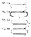
  • FIGs. 1A to 1D are schematic representations showing one exemplary process for manufacturing a silicon wafer and a silicon epitaxial wafer in accordance with the present invention;
  • FIG. 2 is a plot showing thicknesswise variations in the composition and components of a plasma CVD film formed on the back surface of a silicon wafer in Example 1; and
  • FIG. 3 is a plot showing thicknesswise variations in the composition and components of a plasma CVD film formed on the back surface of a silicon wafer in Example 2.
  • DESCRIPTION OF THE INVENTION AND EMBODIMENTS THEREOF
    In reference to the accompanying drawings, the present invention will be described hereinbelow.
    First, an explanation will be given with reference to FIGs. 1A through 1D.
    A silicon wafer 1 is first prepared by a known manufacturing method (FIG. 1A). Here, although a chemically-etched wafer before it is mirror-polished is commonly used as this silicon wafer 1, a mirror-polished wafer which is mirror-polished at one or both sides may be also employed.
    Subsequently, a CVD film 2 is deposited on the back surface of the silicon wafer through use of a CVD apparatus (FIG. 1B). The components and composition of a CVD film to be deposited are changed in the thicknesswise direction of the film. In this event, there are preferably combined more than one layer of an amorphous silicon layer (Si), a silicon oxide layer (SiOx: 0 < suffix x ≦ 2), a silicon nitride layer (SiNz: 0 < suffix z < 1.34), and a silicon oxynitride layer (SiOxNy: 0 < suffix x ≦ 2, and 0 < suffix y < 1.34). More preferably, component x, y, or z in one film is changed in the thicknesswise direction of the CVD film. Such a CVD film is provided with superior gettering and autodoping-prevention capability, and source gases of such a CVD film are easy to obtain.
    The components and composition of the CVD film can be changed in the thicknesswise direction of a CVD film to be deposited by programming the CVD apparatus with regard to the deposition temperature, the deposition pressure, the deposition time, the type of reactive gas, or the flow rate in accordance with the application of the silicon wafer. Accordingly, the CVD film whose components and composition change in the thicknesswise direction thereof can be deposited on a silicon wafer in one process step or in a consecutive manner. In this event, the thickness of a CVD film to be deposited is preferably within the range of 50 to 500 nm. Further, the deposition temperature and pressure are preferably within the range of 100 to 450 °C and 0.1 to 10 torr, respectively.
    As described above, after the CVD film 2 has been deposited on the silicon wafer 1, the front surface and the edge of the silicon wafer are mirror-polished (FIG. 1C). At this time, the CVD film deposited on the front surface of the silicon wafer to be mirror-polished can be finished at a very high speed, whereby the CVD film can be easily removed without impairing the flatness of the silicon wafer by polishing.
    In a case where a mirror-polished wafer whose one or both sides are mirror-polished is used as the silicon wafer on which a CVD film is deposited, and where the front surface of the silicon wafer opposite to the surface on which a CVD film is deposited is mirror-polished, a CVD film is deposited on the back surface of the silicon wafer so as not to pass around to the mirror-polished surface, whereby a step to mirror polish the front surface after the deposition of the CVD film can be omitted.
    Throughout the foregoing procedures, there is obtained a silicon wafer with a gettering layer which has superiorly. persistent gettering capability with respect to a greater variety of types of elements in comparison with the conventional silicon wafer and an autodoping-prevention effect. Further, since the CVD film is formed in one process step, it can be manufactured more inexpensively.
    Even when a silicon monocrystalline thin-film is epitaxially grown on the front surface of the thus-formed silicon wafer through use of a commercially available epitaxial growth apparatus, the prevention of an autodoping phenomenon; i.e., the prevention of incorporation of dopants released from the silicon wafer, facilitates the control of the resistivity of the epitaxial layer even in a case where the silicon wafer contains a high concentration of dopants. There is obtained a silicon epitaxial wafer having an epitaxial layer 3 whose resistivity is the same as originally designed (FIG. 1D).
    EXAMPLES
    Studies were carried out on the gettering capability of the silicon wafer in accordance with the present invention on the persistency of the gettering capability, and on the autodoping-prevention capability of the same at the time of epitaxial growth.
    A silicon monocrystalline rod produced by the Czochralski method [the silicon monocrystal has a (100) main face, a p-type conductivity, and a resistivity of 0.01 Ω · cm] was sliced to obtain four wafers (CZ wafers), which were then subjected to chamfering, lapping, and chemical etching processes.
    Further, a silicon monocrystalline rod produced by the floating zone method [the silicon monocrystal has a (100) main face, an n-type conductivity, and a resistivity of 20 Ω · cm] was sliced to obtain eight wafers (FZ wafers), which were then subjected to chamfering, lapping, and chemical etching processes.
    As shown in Table 1, plasma CVD films (Examples 1 and 2 of the present invention) or a polycrystalline silicon film (Comparative example 1) were formed on one main face of the foregoing wafers, or none of the films were formed on the wafer (Comparative example 2).
    Kinds of wafers FZ wafer CZ wafer
    Evaluated items Gettering capability Persistency of gettering capability Autodoping prevention capability
    Example 1 1 1 1
    Example 2 1 1 1
    Comparative example 1 1 1 1
    Comparative example 2 1 1 1
    1) Example 1
    A plasma CVD film which was comprised of a component Si and O and was grown through use of a plasma CVD apparatus:
    Growth Conditions:
  • Growth temperature: 425 °C,
  • Deposition thickness: 0.5 µm,
  • Pressure in a furnace: 3 torr,
  • Reaction gas: monosilane, dinitrogen oxide,
  • Carrier gas: nitrogen
  • Thicknesswise profile of components-and-composition of the film: shown in FIG. 2
  • 2) Example 2
    A plasma CVD film which was comprised of components Si, O, N and was grown through use of the plasma CVD apparatus: Growth Conditions:
  • Growth temperature: 425 °C,
  • Deposition thickness: 0.5 µm,
  • Pressure in a furnace: 3 torr,
  • Reaction gas: monosilane, dinitrogen oxide, ammonia
  • Carrier gas: nitrogen
  • Thicknesswise profile of components-and-composition of the film: shown in FIG. 3
  • 3) Comparative Example 1
    A polycrystalline silicon film grown through use of a low-pressure CVD apparatus:
    Growth Conditions:
  • Growth temperature: 650 °C,
  • Deposition thickness: 1.5 µm,
  • Pressure in a furnace: 0.1 torr,
  • Reaction gas: monosilane,
  • Carrier gas: hydrogen
  • Subsequently, the other main face of the wafer having a plasma CVD film or polycrystalline silicon firm formed on one main face thereof was polished. Further, one of the two main faces of the wafer on which no film was formed was also polished. As a result, there were manufactured three wafers for each of the four types of silicon wafers; namely, the mirror-polished silicon wafers having three types of gettering layers (Examples 1 and 2 and Comparative example 1) and the mirror-polished silicon wafer without the gettering layer for the purpose of reference (Comparative example 2).
    These silicon wafers were examined in the following manner with regard to the gettering capability, the persistency of the gettering capability, and the autodoping-prevention capability at the time of epitaxial growth.
    1) Gettering Capability
    A solution containing a plurality of heavy metal ions (iron, copper, chrome, and nickel ions) was applied to each front surface of the four types of wafers, so that the wafers were intentionally contaminated. Subsequently, they undergone heat treatment at 1000 °C for 1 hr, whereby the heavy metal ions were diffused into the wafer. Subsequently, after they had been subjected to heat treatment at 650 °C for 10 hrs., the concentration of heavy metals in each silicon wafer with the exception of its gettering layer was measured through use of the DLTS method (Deep Level Transient Spectroscopy) and the ICP-MS method (Inductively-coupled Plasma Mass Spectrometer). While the concentration of each heavy metal contained in the wafer without the gettering layer was used as a standard, the proportion of each heavy metal captured in each gettering layer was calculated from the resultant measurement of the concentration of each heavy metal.
    Table 2 shows the results of such calculation.
    Capability of gettering various heavy metals
    Iron Copper Chromium Nickel
    Example 1 99% 89% 85% 75%
    Example 2 99% 87% 85% 77%
    Comparative example 1 93% 72% 35% 25%
    Comparative example 2 0% 0% 0% 0%
    Table 2 shows that the plasma CVD film in accordance with the present invention exhibits a sufficient gettering effect with respect to chromium and nickel in comparison with the polycrystalline silicon film of the comparative example 1 which exhibits an insufficient gettering effect. Accordingly, it is acknowledged that the plasma CVD film in accordance with the present invention possesses superior gettering capability than that of the polycrystalline silicon film.
    2) Persistency of Gettering Capability
    After the four types of wafers had been subjected to heat treatment at 1050 °C for 1 hr., a solution containing iron ions was applied to the front surface of each of the wafers, so that they were intentionally contaminated, after that, the wafers undergone heat treatment at 1000 °C for 1 hr, whereby iron was diffused into the wafers. Subsequently, after the wafers had been subjected to heat treatment at 650 °C for 10 hrs., the concentration of iron in each wafer with the exception of its gettering layer was measured. While the concentration of iron of the wafer without the gettering layer was used as a reference, the proportion of iron captured by the gettering layer was calculated from the resultant measurement of the concentration of iron.
    Table 3 shows the results of such calculation.
    Gettering capability
    Example 1 90%
    Example 2 90%
    Comparative example 1 70%
    Comparative example 2 0%
    Table 3 shows that the plasma CVD film in accordance with the present invention retains superior gettering capability after having undergone heat treatment in comparison with the polycrystalline silicon film of Comparative example 1; namely, the plasma CVD film is superior in the persistency of gettering capability.
    3) Autodoping-prevention Capability at the time of Epitaxial Growth
    An epitaxial layer was grown on each of the four types of wafers under the following conditions through use of an epitaxial growth apparatus.
  • Growth temperature: 1100°C
  • Epitaxial layer: 10 µm thick,
  • Resistivity: 10 Ω · cm,
  • Conductivity type: P-type
  • In the growth of an epitaxial layer, the four types of wafers were subjected to batch processing one by one so as to prevent the wafers from being affected by autodoping.
    A chip measuring 3 mm was cut out of the center of each of the four types of wafers on which the epitaxial layers were formed. The surface of the epitaxial layer of each chip was obliquely polished (bevel or angle polishing), and the profile of spreading resistance in the interface between the epitaxial layer and the silicon wafer in the depthwise direction was measured through use of a spreading-resistance measurement instrument, whereby a transition width is obtained. Table 4 shows the results of such measurement.
    Example 1 Example 2 Comparative example 1 Comparative example 2
    Transition width 1.4µm 1.4µm 1.6µm 2.5µm
    Table 4 shows that the silicon wafer having the plasma CVD film in accordance with the present invention has a narrower transition width than that of the silicon wafer having the polycrystalline silicon film. It is acknowledged that the plasma CVD film in accordance with the present invention has superior autodoping-prevention capability at the time of epitaxial growth as well as superior gettering capability.
    The present invention is not limited to the above-described embodiments. The above-described embodiments are mere examples, and those having the substantially same structure as that described in the appended claims and providing the similar action and effects are included in the scope of the present invention.

    Claims (8)

    1. A silicon wafer having a CVD film formed on one main face and having the other main face mirror-polished, characterized in that the components and/or composition of the CVD film change in the thicknesswise direction of the film.
    2. A silicon wafer according to Claim 1, characterized in that the CVD film comprises SiOx, wherein the suffix x varies in the range of 0 ≦ x ≦ 2.
    3. A silicon wafer according to Claim 1, characterized in that the CVD film comprises SiNz, wherein the suffix z varies in the range of 0 ≦ z < 1.34.
    4. A silicon wafer according to Claim 1, characterized in that the CVD film comprises SiOxNy, wherein the suffix x varies in the range of 0 ≦ x ≦ 2, while the suffix y varies in the range of 0 ≦ z < 1.34.
    5. A silicon wafer according to any one of Claims 1 -4, characterized in that the CVD film is formed by plasma chemical vapor deposition.
    6. A method of manufacturing a silicon wafer of any one of Claims 1 -5, characterized in that the CVD film is formed by chemical vapor deposition in one process step or in a consecutive manner in such a way that the components and/or composition of the CVD film change in the thicknesswise direction of the film.
    7. A method of manufacturing a silicon wafer according to Claim 6, characterized in that the main face of the silicon wafer on which the CVD film is formed is etched or mirror-polished before formation of the CVD film.
    8. A silicon epitaxial wafer in which a silicon monocrystalline thin-film is epitaxially grown on the mirror-polished main face of the silicon wafer according to any one of Claims 1 - 5.
    EP97306225A 1996-08-19 1997-08-15 Silicon wafer and method of manufacturing the same Withdrawn EP0825639A3 (en)

    Applications Claiming Priority (2)

    Application Number Priority Date Filing Date Title
    JP23587096A JP3454033B2 (en) 1996-08-19 1996-08-19 Silicon wafer and manufacturing method thereof
    JP235870/96 1996-08-19

    Publications (2)

    Publication Number Publication Date
    EP0825639A2 true EP0825639A2 (en) 1998-02-25
    EP0825639A3 EP0825639A3 (en) 1999-05-26

    Family

    ID=16992475

    Family Applications (1)

    Application Number Title Priority Date Filing Date
    EP97306225A Withdrawn EP0825639A3 (en) 1996-08-19 1997-08-15 Silicon wafer and method of manufacturing the same

    Country Status (4)

    Country Link
    US (1) US5998283A (en)
    EP (1) EP0825639A3 (en)
    JP (1) JP3454033B2 (en)
    TW (1) TW346653B (en)

    Cited By (1)

    * Cited by examiner, † Cited by third party
    Publication number Priority date Publication date Assignee Title
    WO2004030060A1 (en) * 2002-09-25 2004-04-08 Siltronic Ag Two layer lto temperature oxide backside seal for a wafer

    Families Citing this family (14)

    * Cited by examiner, † Cited by third party
    Publication number Priority date Publication date Assignee Title
    US6376335B1 (en) * 2000-02-17 2002-04-23 Memc Electronic Materials, Inc. Semiconductor wafer manufacturing process
    JP4270713B2 (en) * 2000-05-09 2009-06-03 信越半導体株式会社 Manufacturing method of silicon epitaxial wafer
    US6715497B2 (en) * 2001-01-02 2004-04-06 International Business Machines Corporation Treatment to eliminate polysilicon defects induced by metallic contaminants
    US6576501B1 (en) 2002-05-31 2003-06-10 Seh America, Inc. Double side polished wafers having external gettering sites, and method of producing same
    JP2004327489A (en) * 2003-04-21 2004-11-18 Shin Etsu Handotai Co Ltd Single-crystal silicon wafer and its manufacturing method
    US7250358B2 (en) * 2004-08-06 2007-07-31 Globitech Incorporated Wafer for preventing the formation of silicon nodules and method for preventing the formation of silicon nodules
    JP5347791B2 (en) * 2009-07-16 2013-11-20 信越半導体株式会社 Manufacturing method of semiconductor epitaxial wafer
    JP5795461B2 (en) * 2009-08-19 2015-10-14 株式会社Sumco Epitaxial silicon wafer manufacturing method
    CN109216157A (en) * 2017-07-04 2019-01-15 上海新昇半导体科技有限公司 The method of back surface of the wafer sealing
    CN109216155A (en) * 2017-07-04 2019-01-15 上海新昇半导体科技有限公司 A kind of method of back surface of the wafer sealing
    CN109216212A (en) * 2017-07-04 2019-01-15 上海新昇半导体科技有限公司 The method of sealing backside chip
    CN109216156B (en) * 2017-07-04 2020-12-15 上海新昇半导体科技有限公司 Method for sealing wafer on back surface
    CN109904070B (en) * 2017-12-11 2021-04-20 有研半导体材料有限公司 Substrate edge processing method for large-diameter wafer
    CN113496871A (en) * 2020-04-03 2021-10-12 重庆超硅半导体有限公司 Back film layer of silicon wafer for epitaxial substrate and manufacturing method thereof

    Citations (3)

    * Cited by examiner, † Cited by third party
    Publication number Priority date Publication date Assignee Title
    EP0120830A2 (en) * 1983-02-14 1984-10-03 MEMC Electronic Materials, Inc. Semiconductor substrate materials having enhanced gettering ability
    DE3717440A1 (en) * 1987-05-23 1988-12-01 Osaka Titanium Semiconductor wafer and method for its fabrication
    JPH042133A (en) * 1990-04-18 1992-01-07 Mitsubishi Electric Corp Crystal sheet

    Family Cites Families (12)

    * Cited by examiner, † Cited by third party
    Publication number Priority date Publication date Assignee Title
    US3663319A (en) * 1968-11-20 1972-05-16 Gen Motors Corp Masking to prevent autodoping of epitaxial deposits
    JPS4929099B1 (en) * 1970-03-27 1974-08-01
    JPS59186331A (en) * 1983-04-04 1984-10-23 モンサント・コンパニ− Method of producing semiconductor substrate
    US4608096A (en) * 1983-04-04 1986-08-26 Monsanto Company Gettering
    US4662956A (en) * 1985-04-01 1987-05-05 Motorola, Inc. Method for prevention of autodoping of epitaxial layers
    US4925809A (en) * 1987-05-23 1990-05-15 Osaka Titanium Co., Ltd. Semiconductor wafer and epitaxial growth on the semiconductor wafer with autodoping control and manufacturing method therefor
    DK170189B1 (en) * 1990-05-30 1995-06-06 Yakov Safir Process for the manufacture of semiconductor components, as well as solar cells made therefrom
    US5296385A (en) * 1991-12-31 1994-03-22 Texas Instruments Incorporated Conditioning of semiconductor wafers for uniform and repeatable rapid thermal processing
    DE4304849C2 (en) * 1992-02-21 2000-01-27 Mitsubishi Electric Corp Semiconductor device and method of manufacturing a semiconductor device
    JPH06104268A (en) * 1992-09-21 1994-04-15 Mitsubishi Electric Corp Semiconductor substrate having gettering effect and its manufacturing method
    JP2908150B2 (en) * 1992-11-27 1999-06-21 日本電気株式会社 SOI substrate structure and manufacturing method thereof
    JP2827885B2 (en) * 1994-02-12 1998-11-25 信越半導体株式会社 Semiconductor single crystal substrate and method of manufacturing the same

    Patent Citations (3)

    * Cited by examiner, † Cited by third party
    Publication number Priority date Publication date Assignee Title
    EP0120830A2 (en) * 1983-02-14 1984-10-03 MEMC Electronic Materials, Inc. Semiconductor substrate materials having enhanced gettering ability
    DE3717440A1 (en) * 1987-05-23 1988-12-01 Osaka Titanium Semiconductor wafer and method for its fabrication
    JPH042133A (en) * 1990-04-18 1992-01-07 Mitsubishi Electric Corp Crystal sheet

    Non-Patent Citations (1)

    * Cited by examiner, † Cited by third party
    Title
    PATENT ABSTRACTS OF JAPAN vol. 016, no. 142 (E-1187), 9 April 1992 & JP 04 002133 A (MITSUBISHI ELECTRIC CORP), 7 January 1992 *

    Cited By (4)

    * Cited by examiner, † Cited by third party
    Publication number Priority date Publication date Assignee Title
    WO2004030060A1 (en) * 2002-09-25 2004-04-08 Siltronic Ag Two layer lto temperature oxide backside seal for a wafer
    KR100713112B1 (en) * 2002-09-25 2007-05-02 실트로닉 아게 Wafer with two layer backside seal and method for forming two layer lto backside seal on wafer
    CN100409407C (en) * 2002-09-25 2008-08-06 硅电子股份公司 Two layer LTO backside seal for a wafer
    US8007914B2 (en) 2002-09-25 2011-08-30 Siltronic Ag Two layer LTO temperature oxide backside seal for a wafer

    Also Published As

    Publication number Publication date
    US5998283A (en) 1999-12-07
    EP0825639A3 (en) 1999-05-26
    TW346653B (en) 1998-12-01
    JPH1064917A (en) 1998-03-06
    JP3454033B2 (en) 2003-10-06

    Similar Documents

    Publication Publication Date Title
    US5998283A (en) Silicon wafer having plasma CVD gettering layer with components/composition changing in depth-wise direction and method of manufacturing the silicon wafer
    EP0635879B1 (en) Process for producing a semiconductor silicon wafer
    US5834363A (en) Method of manufacturing semiconductor wafer, semiconductor wafer manufactured by the same, semiconductor epitaxial wafer, and method of manufacturing the semiconductor epitaxial wafer
    KR100808930B1 (en) Method for producing epitaxially coated silicon wafers
    US20020022351A1 (en) Method for the production of an epitaxially grown semiconductor wafer
    KR20020062225A (en) SINGLE CRYSTAL SiC AND METHOD OF PRODUCING THE SAME AS WELL AS SiC SEMICONDUCTOR DEVICE AND SiC COMPOSITE MATERIAL
    Wong et al. The poly‐single crystalline silicon interface
    JP2003505317A (en) Method of growing epitaxial semiconductor material with improved crystalline properties
    US20080224270A1 (en) Silicon single crystal substrate and manufacture thereof
    TW200525053A (en) Process for producing highly doped semiconductor wafers, and dislocation-free, highly doped semiconductor wafers
    KR960016834B1 (en) Fabricating method of semiconductor substrate
    US5882990A (en) Manufacturing method for wafer slice starting material to optimize extrinsic gettering during semiconductor fabrication
    EP1533402A1 (en) Epitaxial wafer and its manufacturing method
    US5653803A (en) Method of manufacturing a substrate for manufacturing silicon semiconductor elements
    EP0702401B1 (en) Method for producing a semiconductor substrate suitable for IGBTs
    US8329532B2 (en) Process for the simultaneous deposition of crystalline and amorphous layers with doping
    EP0798770B1 (en) Silicon wafer with superimposed polycrystalline silicon films on one main surface and its fabrication method
    US4000020A (en) Vapor epitaxial method for depositing gallium arsenide phosphide on germanium and silicon substrate wafers
    US5634973A (en) Low temperature selective growth of silicon or silicon alloys
    EP3112504B1 (en) Method for producing epitaxial silicon carbide wafer
    JP3344205B2 (en) Method for manufacturing silicon wafer and silicon wafer
    US5970365A (en) Silicon wafer including amorphous silicon layer formed by PCVD and method of manufacturing wafer
    Watts The preparation and properties of elemental semiconductor thin films
    EP0496382B1 (en) Intrinsic gettering for a semiconducteur epitaxial wafer
    EP0709878B1 (en) Method for the preparation of discrete substrate plates of semiconductor silicon wafer

    Legal Events

    Date Code Title Description
    PUAI Public reference made under article 153(3) epc to a published international application that has entered the european phase

    Free format text: ORIGINAL CODE: 0009012

    AK Designated contracting states

    Kind code of ref document: A2

    Designated state(s): DE FR GB IT

    AX Request for extension of the european patent

    Free format text: AL;LT;LV;RO;SI

    PUAL Search report despatched

    Free format text: ORIGINAL CODE: 0009013

    AK Designated contracting states

    Kind code of ref document: A3

    Designated state(s): AT BE CH DE DK ES FI FR GB GR IE IT LI LU MC NL PT SE

    AX Request for extension of the european patent

    Free format text: AL;LT;LV;RO;SI

    17P Request for examination filed

    Effective date: 19991008

    AKX Designation fees paid

    Free format text: DE FR GB IT

    STAA Information on the status of an ep patent application or granted ep patent

    Free format text: STATUS: THE APPLICATION IS DEEMED TO BE WITHDRAWN

    18D Application deemed to be withdrawn

    Effective date: 20030301