EP0823788A2 - Receiving mixer circuit for mobile radio transceiver designed to operate with multiple modulation modes and multiple frequency bands - Google Patents
Receiving mixer circuit for mobile radio transceiver designed to operate with multiple modulation modes and multiple frequency bands Download PDFInfo
- Publication number
- EP0823788A2 EP0823788A2 EP97113570A EP97113570A EP0823788A2 EP 0823788 A2 EP0823788 A2 EP 0823788A2 EP 97113570 A EP97113570 A EP 97113570A EP 97113570 A EP97113570 A EP 97113570A EP 0823788 A2 EP0823788 A2 EP 0823788A2
- Authority
- EP
- European Patent Office
- Prior art keywords
- frequency
- impedance conversion
- receiving mixer
- receive
- gate
- Prior art date
- Legal status (The legal status is an assumption and is not a legal conclusion. Google has not performed a legal analysis and makes no representation as to the accuracy of the status listed.)
- Withdrawn
Links
- 238000006243 chemical reaction Methods 0.000 claims abstract description 30
- 238000010295 mobile communication Methods 0.000 claims description 39
- 230000005540 biological transmission Effects 0.000 claims description 12
- 239000003990 capacitor Substances 0.000 claims description 6
- 239000004065 semiconductor Substances 0.000 claims 1
- 239000000758 substrate Substances 0.000 claims 1
- RDYMFSUJUZBWLH-UHFFFAOYSA-N endosulfan Chemical compound C12COS(=O)OCC2C2(Cl)C(Cl)=C(Cl)C1(Cl)C2(Cl)Cl RDYMFSUJUZBWLH-UHFFFAOYSA-N 0.000 description 12
- 238000010586 diagram Methods 0.000 description 10
- 239000002131 composite material Substances 0.000 description 5
- 230000000694 effects Effects 0.000 description 3
- 230000000903 blocking effect Effects 0.000 description 2
- 238000000034 method Methods 0.000 description 2
Images


Classifications
-
- H—ELECTRICITY
- H03—ELECTRONIC CIRCUITRY
- H03C—MODULATION
- H03C1/00—Amplitude modulation
-
- H—ELECTRICITY
- H04—ELECTRIC COMMUNICATION TECHNIQUE
- H04B—TRANSMISSION
- H04B1/00—Details of transmission systems, not covered by a single one of groups H04B3/00 - H04B13/00; Details of transmission systems not characterised by the medium used for transmission
- H04B1/005—Details of transmission systems, not covered by a single one of groups H04B3/00 - H04B13/00; Details of transmission systems not characterised by the medium used for transmission adapting radio receivers, transmitters andtransceivers for operation on two or more bands, i.e. frequency ranges
- H04B1/0053—Details of transmission systems, not covered by a single one of groups H04B3/00 - H04B13/00; Details of transmission systems not characterised by the medium used for transmission adapting radio receivers, transmitters andtransceivers for operation on two or more bands, i.e. frequency ranges with common antenna for more than one band
- H04B1/0057—Details of transmission systems, not covered by a single one of groups H04B3/00 - H04B13/00; Details of transmission systems not characterised by the medium used for transmission adapting radio receivers, transmitters andtransceivers for operation on two or more bands, i.e. frequency ranges with common antenna for more than one band using diplexing or multiplexing filters for selecting the desired band
-
- H—ELECTRICITY
- H04—ELECTRIC COMMUNICATION TECHNIQUE
- H04B—TRANSMISSION
- H04B1/00—Details of transmission systems, not covered by a single one of groups H04B3/00 - H04B13/00; Details of transmission systems not characterised by the medium used for transmission
- H04B1/005—Details of transmission systems, not covered by a single one of groups H04B3/00 - H04B13/00; Details of transmission systems not characterised by the medium used for transmission adapting radio receivers, transmitters andtransceivers for operation on two or more bands, i.e. frequency ranges
-
- H—ELECTRICITY
- H04—ELECTRIC COMMUNICATION TECHNIQUE
- H04B—TRANSMISSION
- H04B1/00—Details of transmission systems, not covered by a single one of groups H04B3/00 - H04B13/00; Details of transmission systems not characterised by the medium used for transmission
- H04B1/06—Receivers
- H04B1/16—Circuits
- H04B1/26—Circuits for superheterodyne receivers
-
- H—ELECTRICITY
- H04—ELECTRIC COMMUNICATION TECHNIQUE
- H04B—TRANSMISSION
- H04B1/00—Details of transmission systems, not covered by a single one of groups H04B3/00 - H04B13/00; Details of transmission systems not characterised by the medium used for transmission
- H04B1/38—Transceivers, i.e. devices in which transmitter and receiver form a structural unit and in which at least one part is used for functions of transmitting and receiving
- H04B1/40—Circuits
- H04B1/403—Circuits using the same oscillator for generating both the transmitter frequency and the receiver local oscillator frequency
- H04B1/406—Circuits using the same oscillator for generating both the transmitter frequency and the receiver local oscillator frequency with more than one transmission mode, e.g. analog and digital modes
Definitions
- the present invention relates to a mobile communication radio transceiver designed to operate with multiple modulation modes and multiple frequency bands, wherein the mobile communication radio transceiver operates by switching frequency bands or modulation modes in a plurality of mobile communication systems among which different radio frequency bands and different modulation modes are used.
- the invention also relates to a receiving mixer circuit for such a mobile communication radio transceiver.
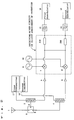
- Figure 5 shows an example of a prior art mobile radio transceiver configuration for implementing simultaneously two mobile communication systems that use two different modulation modes with the same frequency band and a mobile communication system that uses either of tow modulation modes and two different frequency bands.
- Figure 5 shows the block diagram for a multi-mode and multi-band mobile radio transceiver that operates by switching among a mobile communication system A which uses a first radio frequency band and a first modulation mode, a mobile communication system B which uses a second radio frequency band and employs the same first modulation mode as the system A, and a mobile communication system C which uses the same second radio frequency band as the system B and employs a second modulation mode.
- reference numeral 1 is an antenna
- 2 is a frequency select switch for switching between the first and second radio frequency bands
- 3 is a first duplexer for the first radio frequency band
- 4 is a second duplexer for the second radio frequency band
- 5 is a first low-noise amplifier for a first receive frequency band
- 6 is a second low-noise amplifier for a second receive frequency band
- 7 is a first receiving mixer for the first receive frequency band
- 8 is a second receiving mixer for the second receive frequency band
- 9 is a first local oscillator for the first radio frequency band
- 10 is a second local oscillator for the second radio frequency band
- 13 is a first intermediate-frequency filter with a first receive bandwidth corresponding to a first receive intermediate frequency of the first modulation mode
- 14 is a second intermediate-frequency filter with a second receive bandwidth corresponding to a second receive intermediate frequency of the second modulation mode
- 11 and 12 are select switches for directing the first and second receive intermediate-frequency signals to the corresponding intermediate-frequency filters
- the second receive bandwidth 30 KHz.
- a signal on the first radio frequency band transmitted from a base radio transceiver station is received by the antenna 1, and by switching the frequency select switch 2 to the A side, the received signal is fed into the first duplexer 3 where it is separated from the transmitting signal.
- the separated received signal is amplified by the first low-noise amplifier 5, and converted by the first receiving mixer 7 to the first receive intermediate frequency f1IF.
- the output signal of the first receiving mixer 7 is fed into the first intermediate-frequency filter 13. After passing through the first intermediate-frequency filter 13, the signal is input to the first demodulator 15 for demodulation.
- a signal on the second radio frequency band transmitted from a base radio transceiver station is received by the antenna 1, and by switching the frequency select switch 2 to the B side, the received signal is fed into the second duplexer 4 where it is separated from the transmitting signal.
- the separated received signal is amplified by the second low-noise amplifier 6, and converted by the second receiving mixer 8 to the first receive intermediate frequency f1IF.
- the output signal of the second receiving mixer 8 is fed into the first intermediate-frequency filter 13. After passing through the first intermediate-frequency filter 13, the signal is input to the first demodulator 15 for demodulation.
- a signal on the second radio frequency band transmitted from a base radio transceiver station is received by the antenna 1, and by switching the frequency select switch 2 to the B side, the received signal is fed into the second duplexer 4 where it is separated from the transmitting signal.
- the separated received signal is amplified by the second low-noise amplifier 6, and converted by the second receiving mixer 8 to the second receive intermediate frequency f2IF.
- the output signal of the second receiving mixer 8 is fed into the second intermediate-frequency filter 14. After passing through the second intermediate-frequency filter 14, the signal is input to the second demodulator 16 for demodulation.
- the receiving mixer circuit of the above prior art configuration has had the problem that it is disadvantageous in terms of the size and cost of the circuit.
- the present invention has been devised to overcome the problem of the prior art, and an object of the invention is to provide a receiving mixer circuit that is inexpensive and small in circuit size by using impedance conversion circuits and thus eliminating the need for select switches.
- the present invention provides a receiving mixer for a mobile radio transceiver designed to operate with multiple modulations and multiple frequency bands , comprising: a plurality of mixers each for converting a received radio frequency signal to an intermediate frequency; a common connection part to which output terminals of said mixers are connected in common; a plurality of impedance conversion means connected to said common connection part; and output terminals for said impedance conversion means; wherein said mixers are equal in number to the kinds of frequencies of said received radio frequency signal, the number of kinds of said intermediate frequencies is the same as the number of modulation modes that the frequency of said received radio frequency signal has, the number of said impedance conversion means is the same as the number of kinds of said intermediate frequencies, and each of said impedance conversion means passes only one uniquely predetermined frequency out of said kinds of intermediate frequencies.
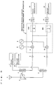
- Figure 1 is a simplified block diagram of a mobile radio transceiver according to a first embodiment of the present invention, designed to operate in a plurality of mobile communication systems among which two frequency bands and two transmission systems are used.
- FIG. 2 is a simplified block diagram of a mobile radio transceiver according to a second embodiment of the present invention, designed to operate in a plurality of mobile communication systems among which two frequency bands and two transmission systems are used.
- Figure 3 is a simplified block diagram of a mobile radio transceiver according to a third embodiment of the present invention, designed to operate in a plurality of mobile communication systems among which two frequency bands and two transmission systems are used.
- Figure 4 is a detailed circuit diagram of a receiving mixer using dual-gate FETs according to a fourth embodiment of the present invention.
- Figure 5 is a simplified block diagram of a mobile radio transceiver according to prior art, designed to operate in a plurality of mobile communication systems among which two frequency bands and two transmission systems are used.
- the embodiments hereinafter described deal with the configuration of a composite mobile radio transceiver for use in mobile communication systems among which two modulation modes and two frequency band methods are used, wherein the composite mobile radio transceiver operates by switching among a mobile communication system A which uses the first radio frequency band and the first modulation mode, a mobile communication system B which uses the second radio frequency band and employs the same first modulation mode as the mobile communication system A, and a mobile communication system C which uses the same second radio frequency band as the mobile communication system B and employs the second modulation mode.
- Figure 1 shows the block diagram for a first embodiment of the present invention.
- reference numeral 1 is an antenna
- 2 is a frequency select switch for switching between the first and second radio frequency bands
- 3 is a first duplexer for the first radio frequency band
- 4 is a second duplexer for the second radio frequency band
- 5 is a first low-noise amplifier for a first receive frequency band
- 6 is a second low-noise amplifier for a second receive frequency band
- 7 is a first receiving mixer for the first receive frequency band
- 8 is a second receiving mixer for the second receive frequency band
- 9 is a first local oscillator for the first radio frequency band
- 10 is a second local oscillator for the second radio frequency band
- 13 is a first intermediate-frequency filter having a first receive bandwidth for passing a first receive intermediate frequency of the first modulation mode
- 14 is a second intermediate-frequency filter having a second receive bandwidth for passing a second receive intermediate frequency of the second modulation mode
- 15 is a first demodulator for the
- the second receive bandwidth 30 KHz.
- a signal on the first radio frequency band transmitted from a base radio transceiver station is received by the antenna 1, and by switching the frequency select switch 2 to the A side, the received signal is fed into the first duplexer 3 where it is separated from the transmitting signal.
- the separated received signal is amplified by the first low-noise amplifier 5, and converted by the first receiving mixer 7 to the receive intermediate frequency f1IF of the first modulation mode.
- the phase ⁇ 1 of the first phaser (phase shifter) 119 is rotated so as to increase the impedance to the second receive intermediate frequency f2IF without impairing the pass characteristic of the first receive intermediate frequency f1IF.
- the phase ⁇ 2 of the second phaser (phase shifter) 120 is rotated so as to increase the impedance to the receive intermediate frequency f1IF of the first modulation mode to block the output of the first receive intermediate frequency while not impairing the pass characteristic of the second receive intermediate frequency f2IF and thus allowing it to pass through for output.
- the output signal of the first receiving mixer 7 is input to the first intermediate-frequency filter 13 having the bandwidth W1 corresponding to the receive intermediate frequency f1IF of the first modulation mode. After passing through the first intermediate-frequency filter 13, the signal is input to the first demodulator 15 for demodulation.
- a signal on the second radio frequency band transmitted from a base radio transceiver station is received by the antenna 1, and by switching the frequency select switch 2 to the B side, the received signal is fed into the second duplexer 4 where it is separated from the transmitting signal.
- the separated received signal is amplified by the second low-noise amplifier 6, and converted by the second receiving mixer 8 to the receive intermediate frequency f1IF of the first modulation mode.
- the output signal (first receive intermediate frequency) of the second receiving mixer 8 is input to the first and second phasers (phase shifters) operating on the principles described for the operation of the mobile communication system A, so that only the first receive intermediate frequency f1IF is input to the first intermediate-frequency filter 13 having the bandwidth W1 corresponding to the receive intermediate frequency f1IF of the first modulation mode. After passing through the first intermediate-frequency filter 13, the signal is input to the first demodulator 15 for demodulation.
- a signal on the second radio frequency band transmitted from a base radio transceiver station is received by the antenna 1, and by switching the frequency select switch 2 to the B side, the received signal is fed into the second duplexer 4 where it is separated from the transmitting signal.
- the separated received signal is amplified by the second low-noise amplifier 6, and by adjusting the second local oscillator 10, the signal is converted by the second receiving mixer 8 to the receive intermediate frequency f2IF of the second modulation mode.
- the output signal (second receive intermediate frequency) of the second receiving mixer 8 is input to the first and second phasers (phase shifters) operating on the principles described for the operation of the mobile communication system A, so that only the second receive intermediate frequency f2IF is input to the second intermediate-frequency filter 14 having the bandwidth W2 corresponding to the receive intermediate frequency f2IF of the second modulation mode. After passing through the second intermediate-frequency filter 14, the signal is input to the second demodulator 16 for demodulation.
- Figure 2 shows the block diagram for a second embodiment of the present invention.
- reference numeral 219 is a first transmission line corresponding to the first phaser (phase shifter) 119 as an impedance conversion circuit in the first embodiment
- 220 is a second transmission line corresponding to the second phaser (phase shifter) 120 as an impedance conversion circuit in Figure 1.
- the configuration is the same as that of the first embodiment, and therefore, a detailed explanation will be omitted here.
- the transmission lines are capable of the same impedance conversion as achieved by the phasers (phase shifters) of the first embodiment, and the same effect can be obtained by the use of these transmission lines.
- Figure 3 shows the block diagram for a third embodiment of the present invention.
- reference numeral 319 is a first lumped-constant circuit corresponding to the first phaser (phase shifter) 119 as an impedance conversion circuit in the first embodiment
- 320 is a second lumped-constant circuit corresponding to the second phaser (phase shifter) 120 as an impedance conversion circuit in the first embodiment.
- the configuration is the same as that of the first embodiment, and therefore, a detailed explanation will be omitted here.
- the same effect as achieved in the first and second embodiments can be obtained by constructing the first lumped-constant circuit 319 as a high-pass filter circuit that passes the receive intermediate frequency of 180 MHz but blocks the receive intermediate frequency of 90 MHz, and the second lumped-constant circuit 320 as a low-pass filter circuit that passes the receive intermediate frequency of 90 MHz but blocks the receive intermediate frequency of 180 MHz.
- first, second, and third embodiments has dealt with the configuration of a mobile radio transceiver operating in three composite mobile communication systems among which two modulation modes and two frequency bands are used, but it will be recognized that similar configurations can be fabricated for four composite mobile communication systems among which two modulation modes and two frequency bands are used, or for other composite mobile communication systems among which three or more modulation modes and three or more frequency bands are used.
- reference numeral 401 is a first receive frequency matching circuit
- 402 is a first local oscillator frequency matching circuit
- 403 is a second receive frequency matching circuit
- 404 is a second local oscillator frequency matching circuit
- 405 is a first dual-gate FET
- 406 is a second dual-gate FET
- 407 is a first first-gate-biasing circuit
- 408 is a first second-gate-biasing circuit
- 409 is a second first-gate-biasing circuit
- 410 is a second second-gate-biasing circuit
- 411 is a first drain-biasing circuit
- 412 is a second drain-biasing circuit
- 413 is a first receive intermediate frequency matching circuit
- 414 is a second receive intermediate frequency matching circuit
- 415 and 416 are DC-cut capacitors
- 417 is a first impedance conversion circuit
- 418 is a second impedance conversion circuit
- 419 is a first local oscillator frequency input terminal
- the second receive bandwidth 30 KHz.
- a dual-gate FET mixer is constructed by connecting the matching circuit 401 and biasing circuit 407 to the first gate of the first dual-gate FET 405, the matching circuit 402 and biasing circuit 408 to the second gate, and the matching circuit 413 and biasing circuit 411 to the drain.
- the first gate of the first dual-gate FET 405 is supplied with a signal of the first receive frequency f1RX input via the terminal 420 and passed through the matching circuit 401, while the second gate thereof is supplied with a signal of the first local oscillator frequency f1LO input via the terminal 419 and passed through the matching circuit 402.
- a dual-gate FET mixer is constructed by connecting the matching circuit 403 and biasing circuit 409 to the first gate of the second dual-gate FET 406, the matching circuit 404 and biasing circuit 410 to the second gate, and the matching circuit 414 and biasing circuit 412 to the drain.
- the first gate of the second dual-gate FET 406 is supplied with a signal of the second receive frequency f2RX input via the terminal 422 and passed through the matching circuit 403, while the second gate thereof is supplied with a signal of the second local oscillator frequency f2LO input via the terminal 421 and passed through the matching circuit 404.
- the output signal of the first receiving mixer for the mobile communication system B is output at the terminal 423
- the output signal of the second receiving mixer for the mobile communication system C is output at the terminal 424.
- the present invention has the effect of being able to achieve a receiving mixer circuit that is inexpensive, small in circuit size, and does not need control by select switches as required in the prior art, for a mobile radio transceiver designed to operate in mobile communication systems among which multiple modulation modes and multiple frequency band methods are used.
Landscapes
- Engineering & Computer Science (AREA)
- Computer Networks & Wireless Communication (AREA)
- Signal Processing (AREA)
- Transceivers (AREA)
- Superheterodyne Receivers (AREA)
Abstract
Description
Figure 5 shows the block diagram for a multi-mode and multi-band mobile radio transceiver that operates by switching among a mobile communication system A which uses a first radio frequency band and a first modulation mode, a mobile communication system B which uses a second radio frequency band and employs the same first modulation mode as the system A, and a mobile communication system C which uses the same second radio frequency band as the system B and employs a second modulation mode.
The separated received signal is amplified by the first low-
Claims (8)
- A receiving mixer for a mobile radio transceiver designed to operate with multiple modulation modes and multiple frequency bands, comprising: a plurality of mixers each for converting a received radio frequency signal to an intermediate frequency; a common connection part to which output terminals of said mixers are connected in common; a plurality of impedance conversion means connected to said common connection part; and output terminals for said impedance conversion means; wherein said mixers are equal in number to the kinds of frequencies of said received radio frequency signal, the number of kinds of said intermediate frequencies is the same as the number of modulation modes that the frequency of said received radio frequency signal has, the number of said impedance conversion means is the same as the number of kinds of said intermediate frequencies, and each of said impedance conversion means passes only one uniquely predetermined frequency out of said kinds of intermediate frequencies.
- A receiving mixer circuit according to claim 1, wherein phasers (phase shifters) are used as said impedance conversion circuits.
- A receiving mixer circuit according to claim 1, wherein transmission lines are used as said impedance conversion circuits.
- A receiving mixer circuit according to claim 1, wherein lumped-constant circuits are used as said impedance conversion circuits.
- A receiving mixer circuit according to any one of claims 1 to 4, wherein said mixer uses a dual-gate FET whose source is grounded, whose first gate is connected to a receive frequency matching means and a first gate bias supplying means, whose second gate is connected to a local oscillator frequency matching means and a second gate bias supplying means, and whose drain is connected to a receive intermediate frequency matching means and a drain bias supplying means.
- A receiving mixer circuit according to claim 5, wherein said dual-gate FET, said receive frequency matching means, said bias supplying means, and said impedance conversion circuits are fabricated on the same semiconductor substrate.
- A receiving mixer circuit according to claim 5 or 6, wherein the source of said dual-gate FET is connected to a resistor and a capacitor in parallel, whose other ends are grounded to bias the first and second gates of said dual-gate FET to ground potential.
- A mobile communication radio transceiver comprising: a receiving mixer circuit according to any one of claims 1 to 7; demodulating means for demodulating the outputs of said impedance conversion means; and a speaker for converting the demodulated signals into sound.
Applications Claiming Priority (3)
| Application Number | Priority Date | Filing Date | Title |
|---|---|---|---|
| JP8209506A JPH1056392A (en) | 1996-08-08 | 1996-08-08 | Receiving mixer circuit for multi-transmission-system and multi-frequency-band mobile radio equipment |
| JP209506/96 | 1996-08-08 | ||
| JP20950696 | 1996-08-08 |
Publications (2)
| Publication Number | Publication Date |
|---|---|
| EP0823788A2 true EP0823788A2 (en) | 1998-02-11 |
| EP0823788A3 EP0823788A3 (en) | 2002-10-30 |
Family
ID=16573936
Family Applications (1)
| Application Number | Title | Priority Date | Filing Date |
|---|---|---|---|
| EP97113570A Withdrawn EP0823788A3 (en) | 1996-08-08 | 1997-08-06 | Receiving mixer circuit for mobile radio transceiver designed to operate with multiple modulation modes and multiple frequency bands |
Country Status (5)
| Country | Link |
|---|---|
| US (1) | US6006080A (en) |
| EP (1) | EP0823788A3 (en) |
| JP (1) | JPH1056392A (en) |
| KR (1) | KR100432801B1 (en) |
| CN (1) | CN1110124C (en) |
Cited By (7)
| Publication number | Priority date | Publication date | Assignee | Title |
|---|---|---|---|---|
| WO1999023762A1 (en) * | 1997-11-03 | 1999-05-14 | Harris Corporation | Reconfigurable radio system architecture |
| WO2000072456A1 (en) * | 1999-05-24 | 2000-11-30 | Nokia Mobile Phones Limited | Multi-frequency band, multi-mode radio receiver, and associated method, having shared circuit elements |
| US6343207B1 (en) * | 1998-11-03 | 2002-01-29 | Harris Corporation | Field programmable radio frequency communications equipment including a configurable if circuit, and method therefor |
| WO2008000336A1 (en) * | 2006-06-29 | 2008-01-03 | Continental Automotive France | Car radio comprising at least one first reception channel and a second reception channel and corresponding car radio |
| US8768408B2 (en) | 1998-11-26 | 2014-07-01 | Nokia Corporation | Method and arrangement for transmitting and receiving RF signals through various radio interfaces of communication systems |
| CN104218971A (en) * | 2014-09-26 | 2014-12-17 | 四川九州电子科技股份有限公司 | Radio frequency circuit compatible with three transmission modes |
| US10476865B2 (en) | 2001-10-26 | 2019-11-12 | Blackberry Limited | System and method for controlling configuration settings for mobile communication devices and services |
Families Citing this family (15)
| Publication number | Priority date | Publication date | Assignee | Title |
|---|---|---|---|---|
| JP3180735B2 (en) * | 1997-10-22 | 2001-06-25 | 松下電器産業株式会社 | Wireless terminal with transmission timing correction function and method of manufacturing the same |
| AU2003205477A1 (en) * | 2002-02-25 | 2003-09-09 | Sirific Wireless Corporation | Frequency down converter using a multitone local oscillator |
| KR100472484B1 (en) * | 2002-12-10 | 2005-03-10 | 삼성전자주식회사 | Apparatus and method for radio signal parallel processing |
| TWI225332B (en) * | 2003-05-20 | 2004-12-11 | Mediatek Inc | Multi-band low noise amplifier |
| TWI345369B (en) * | 2004-01-28 | 2011-07-11 | Mediatek Inc | High dynamic range time-varying integrated receiver for elimination of off-chip filters |
| US7796956B2 (en) * | 2005-05-03 | 2010-09-14 | Telefonaktiebolaget L M Ericsson (Publ) | Receiver for a multi-antenna, multi-band radio |
| KR100646314B1 (en) | 2005-12-16 | 2006-11-23 | 삼성전자주식회사 | Multi-input multi-frequency synthesizing apparatus and method for multi-band rf receiver |
| US7809349B1 (en) * | 2006-10-18 | 2010-10-05 | Rf Micro Devices, Inc. | Radio frequency filter using intermediate frequency impedance translation |
| JP2009060215A (en) * | 2007-08-30 | 2009-03-19 | Sharp Corp | High frequency module, and mobile phone terminal and electronics using it |
| US8515373B2 (en) * | 2011-09-30 | 2013-08-20 | Silicon Laboratories Inc. | Apparatus for providing reference signals and associated methods |
| US8975966B2 (en) * | 2012-03-07 | 2015-03-10 | Qualcomm Incorporated | Shared bypass capacitor matching network |
| CN105099478B (en) * | 2015-08-21 | 2018-09-04 | 小米科技有限责任公司 | Improve the device and method of radio frequency link receiving sensitivity |
| EP3211802B1 (en) * | 2016-02-26 | 2019-01-02 | Nxp B.V. | Multi-mode transceiver arrangement |
| CN106788322A (en) * | 2016-12-21 | 2017-05-31 | 北京中科飞鸿科技有限公司 | A kind of high performance mini binary channels hybrid integrated filtration module |
| CN107132426A (en) * | 2017-05-02 | 2017-09-05 | 上海德科电子仪表有限公司 | A kind of car antenna measurement and analysis switching device |
Citations (2)
| Publication number | Priority date | Publication date | Assignee | Title |
|---|---|---|---|---|
| US5054114A (en) * | 1988-09-27 | 1991-10-01 | Rockwell International Corporation | Broadband RF transmit/receive switch |
| EP0465315A1 (en) * | 1990-07-04 | 1992-01-08 | Matra Communication | Device for connecting an antenna to radio transceivers |
Family Cites Families (6)
| Publication number | Priority date | Publication date | Assignee | Title |
|---|---|---|---|---|
| US2964622A (en) * | 1957-10-21 | 1960-12-13 | Sylvania Electric Prod | Image suppressed superheterodyne receiver |
| US3070747A (en) * | 1958-09-02 | 1962-12-25 | Microwave Engineering Lab Inc | Image rejection systems |
| CA1112300A (en) * | 1978-01-23 | 1981-11-10 | Gerald J.P. Lo | Circuit and method for reducing polarization crosstalk caused by rainfall |
| JPH0638567B2 (en) * | 1985-02-08 | 1994-05-18 | 株式会社日立製作所 | Frequency converter |
| JP2546331B2 (en) * | 1988-04-26 | 1996-10-23 | ソニー株式会社 | FM / AM receiver |
| US4926500A (en) * | 1988-08-10 | 1990-05-15 | Hughes Aircraft Company | Frequency converter |
-
1996
- 1996-08-08 JP JP8209506A patent/JPH1056392A/en active Pending
-
1997
- 1997-08-06 EP EP97113570A patent/EP0823788A3/en not_active Withdrawn
- 1997-08-07 KR KR1019970037777A patent/KR100432801B1/en not_active IP Right Cessation
- 1997-08-08 US US08/910,940 patent/US6006080A/en not_active Expired - Fee Related
- 1997-08-08 CN CN97117386A patent/CN1110124C/en not_active Expired - Fee Related
Patent Citations (2)
| Publication number | Priority date | Publication date | Assignee | Title |
|---|---|---|---|---|
| US5054114A (en) * | 1988-09-27 | 1991-10-01 | Rockwell International Corporation | Broadband RF transmit/receive switch |
| EP0465315A1 (en) * | 1990-07-04 | 1992-01-08 | Matra Communication | Device for connecting an antenna to radio transceivers |
Cited By (18)
| Publication number | Priority date | Publication date | Assignee | Title |
|---|---|---|---|---|
| WO1999023761A1 (en) * | 1997-11-03 | 1999-05-14 | Harris Corporation | A field programmable radio frequency communications equipment including a configurable if circuit and method therefor |
| US6091765A (en) * | 1997-11-03 | 2000-07-18 | Harris Corporation | Reconfigurable radio system architecture |
| US6389078B1 (en) | 1997-11-03 | 2002-05-14 | Harris Corporation | Configurable circuits for field programmable radio frequency communications equipment and methods therefor |
| US6539052B1 (en) | 1997-11-03 | 2003-03-25 | Harris Corporation | System for accelerating the reconfiguration of a transceiver and method therefor |
| WO1999023762A1 (en) * | 1997-11-03 | 1999-05-14 | Harris Corporation | Reconfigurable radio system architecture |
| US6343207B1 (en) * | 1998-11-03 | 2002-01-29 | Harris Corporation | Field programmable radio frequency communications equipment including a configurable if circuit, and method therefor |
| US8768408B2 (en) | 1998-11-26 | 2014-07-01 | Nokia Corporation | Method and arrangement for transmitting and receiving RF signals through various radio interfaces of communication systems |
| US9270301B2 (en) | 1998-11-26 | 2016-02-23 | Nokia Technologies Oy | Method and arrangement for transmitting and receiving RF signals through various radio interfaces of communication systems |
| US8838049B1 (en) | 1998-11-26 | 2014-09-16 | Nokia Corporation | Method and arrangement for transmitting and receiving RF signals through various radio interfaces of communication systems |
| CN1332510C (en) * | 1999-05-24 | 2007-08-15 | 诺基亚有限公司 | Multi-frequency band, multi-mode radio receiver, and associated method, having shared circuit elements |
| CN101098153B (en) * | 1999-05-24 | 2012-02-22 | 诺基亚有限公司 | Multi-frequency band, multi-mode radio receiver, and associated method, having shared circuit elements |
| EP1838005A1 (en) * | 1999-05-24 | 2007-09-26 | Nokia Corporation | Multi-Frequency band, multi-mode radio receiver, and associated method, having shared circuit elements |
| US6292474B1 (en) | 1999-05-24 | 2001-09-18 | Nokia Mobile Phones Limited | Multi-frequency band nyktu-mode radio receiver and associated method having shared circuit elements |
| WO2000072456A1 (en) * | 1999-05-24 | 2000-11-30 | Nokia Mobile Phones Limited | Multi-frequency band, multi-mode radio receiver, and associated method, having shared circuit elements |
| US10476865B2 (en) | 2001-10-26 | 2019-11-12 | Blackberry Limited | System and method for controlling configuration settings for mobile communication devices and services |
| WO2008000336A1 (en) * | 2006-06-29 | 2008-01-03 | Continental Automotive France | Car radio comprising at least one first reception channel and a second reception channel and corresponding car radio |
| FR2903251A1 (en) * | 2006-06-29 | 2008-01-04 | Siemens Vdo Automotive Sas | AUTORADIO COMPRISING AT LEAST ONE FIRST RECEIVING CHAIN AND A SECOND RECEIVING CHAIN AND AUTORADIO CORRESPONDING |
| CN104218971A (en) * | 2014-09-26 | 2014-12-17 | 四川九州电子科技股份有限公司 | Radio frequency circuit compatible with three transmission modes |
Also Published As
| Publication number | Publication date |
|---|---|
| US6006080A (en) | 1999-12-21 |
| CN1176527A (en) | 1998-03-18 |
| JPH1056392A (en) | 1998-02-24 |
| EP0823788A3 (en) | 2002-10-30 |
| KR19980018483A (en) | 1998-06-05 |
| KR100432801B1 (en) | 2004-07-16 |
| CN1110124C (en) | 2003-05-28 |
Similar Documents
| Publication | Publication Date | Title |
|---|---|---|
| US6006080A (en) | Receiving mixer circuit for mobile radio transceiver designed to operate with multiple modulation modes and multiple frequency bands | |
| US7231189B2 (en) | Transmit and/or receive channel communication system with switchably coupled multiple filtering components | |
| US5634200A (en) | Antenna duplexer and transmitting/receiving apparatus using the same | |
| US7714654B2 (en) | Amplifier and amplifier gain adjustment circuitry using current steering, and multimode communication device containing same | |
| US5878332A (en) | Multiple frequency RF transceiver | |
| US4492960A (en) | Switching mixer | |
| US6134427A (en) | Using a single low-noise amplifier in a multi-band wireless station | |
| AU678538B2 (en) | Digital radio link system and radio link terminal | |
| US7319850B2 (en) | Low noise block downconverter converting received signal to intermediate frequency signal | |
| EP0597653B1 (en) | Radio frequency circuit for a time division multiple access system | |
| JP5702722B2 (en) | Dual mode mixer | |
| JP2002171194A (en) | Radio equipment, base radio station equipped therewith, portable information terminal and radio communication system incorpolating them | |
| WO2000051257A1 (en) | Radio terminal device | |
| JPH10256809A (en) | Electronic tuning polar filter | |
| JPH09275356A (en) | Plural mode mobile radio equipment | |
| JPH09261104A (en) | Mobile radio equipment operated in plural modes | |
| JPH10303830A (en) | Internal loopback test circuit for radio equipment | |
| KR100677851B1 (en) | Wireless Transceiver apparatus having Transceiver route by one Mixer and band pass filter, and the ASK modulation for data transmitting and frequency conversion in the receving | |
| JPH06216803A (en) | Radio equipment | |
| JPS61199306A (en) | Frequency converter | |
| KR100212054B1 (en) | Transceiver circuits with common used inter frequency | |
| KR200380075Y1 (en) | Wireless Transceiver apparatus having Transceiver route by one Mixer and band pass filter | |
| JP2004180135A (en) | Multi-frequency radio transmitter and receiver | |
| JP2000269832A (en) | Radio transmission device, radio reception device and radio communication system | |
| GB2194110A (en) | Reflex microwave amplifier |
Legal Events
| Date | Code | Title | Description |
|---|---|---|---|
| PUAI | Public reference made under article 153(3) epc to a published international application that has entered the european phase |
Free format text: ORIGINAL CODE: 0009012 |
|
| AK | Designated contracting states |
Kind code of ref document: A2 Designated state(s): AT BE CH DE DK ES FI FR GB GR IE IT LI LU MC NL PT SE |
|
| PUAL | Search report despatched |
Free format text: ORIGINAL CODE: 0009013 |
|
| AK | Designated contracting states |
Kind code of ref document: A3 Designated state(s): AT BE CH DE DK ES FI FR GB GR IE IT LI LU MC NL PT SE |
|
| 17P | Request for examination filed |
Effective date: 20021028 |
|
| 17Q | First examination report despatched |
Effective date: 20030122 |
|
| AKX | Designation fees paid |
Designated state(s): DE FR GB |
|
| STAA | Information on the status of an ep patent application or granted ep patent |
Free format text: STATUS: THE APPLICATION IS DEEMED TO BE WITHDRAWN |
|
| 18D | Application deemed to be withdrawn |
Effective date: 20030820 |