EP0823041B1 - Colour detection method - Google Patents
Colour detection method Download PDFInfo
- Publication number
- EP0823041B1 EP0823041B1 EP96910142A EP96910142A EP0823041B1 EP 0823041 B1 EP0823041 B1 EP 0823041B1 EP 96910142 A EP96910142 A EP 96910142A EP 96910142 A EP96910142 A EP 96910142A EP 0823041 B1 EP0823041 B1 EP 0823041B1
- Authority
- EP
- European Patent Office
- Prior art keywords
- colour
- article
- measured
- spectra
- chip
- Prior art date
- Legal status (The legal status is an assumption and is not a legal conclusion. Google has not performed a legal analysis and makes no representation as to the accuracy of the status listed.)
- Expired - Lifetime
Links
- 238000001514 detection method Methods 0.000 title claims description 9
- 238000000034 method Methods 0.000 claims abstract description 31
- 238000001228 spectrum Methods 0.000 claims description 20
- 239000003086 colorant Substances 0.000 claims description 7
- 238000005259 measurement Methods 0.000 claims description 4
- 208000001613 Gambling Diseases 0.000 abstract description 7
- 230000003287 optical effect Effects 0.000 description 8
- 238000010586 diagram Methods 0.000 description 4
- 238000009825 accumulation Methods 0.000 description 1
- 230000001419 dependent effect Effects 0.000 description 1
- 230000000694 effects Effects 0.000 description 1
- 229910052736 halogen Inorganic materials 0.000 description 1
- 150000002367 halogens Chemical class 0.000 description 1
- 230000010354 integration Effects 0.000 description 1
- 238000012986 modification Methods 0.000 description 1
- 230000004048 modification Effects 0.000 description 1
- 230000003595 spectral effect Effects 0.000 description 1
Images

Classifications
-
- G—PHYSICS
- G01—MEASURING; TESTING
- G01J—MEASUREMENT OF INTENSITY, VELOCITY, SPECTRAL CONTENT, POLARISATION, PHASE OR PULSE CHARACTERISTICS OF INFRARED, VISIBLE OR ULTRAVIOLET LIGHT; COLORIMETRY; RADIATION PYROMETRY
- G01J3/00—Spectrometry; Spectrophotometry; Monochromators; Measuring colours
- G01J3/46—Measurement of colour; Colour measuring devices, e.g. colorimeters
- G01J3/50—Measurement of colour; Colour measuring devices, e.g. colorimeters using electric radiation detectors
- G01J3/502—Measurement of colour; Colour measuring devices, e.g. colorimeters using electric radiation detectors using a dispersive element, e.g. grating, prism
-
- G—PHYSICS
- G01—MEASURING; TESTING
- G01J—MEASUREMENT OF INTENSITY, VELOCITY, SPECTRAL CONTENT, POLARISATION, PHASE OR PULSE CHARACTERISTICS OF INFRARED, VISIBLE OR ULTRAVIOLET LIGHT; COLORIMETRY; RADIATION PYROMETRY
- G01J3/00—Spectrometry; Spectrophotometry; Monochromators; Measuring colours
- G01J3/46—Measurement of colour; Colour measuring devices, e.g. colorimeters
- G01J3/50—Measurement of colour; Colour measuring devices, e.g. colorimeters using electric radiation detectors
- G01J3/504—Goniometric colour measurements, for example measurements of metallic or flake based paints
Definitions
- This invention concerns a method of colour detection and also a method of sorting different coloured articles; and particularly but not exclusively a method of detecting the colour of and sorting gambling chips, and other rotary symetrical coloured articles.
- WOA-89/04468 discloses an apparatus for colour control in which an average value of the colour of an object is measured.
- EP-A-0315039 measures the colour of an object moving on a conveyor with a sensor, the output of which corresponds to a time and space integrated intensity in a specific wavelength band.
- the method comprises sensing the colour of the article at a plurality of places on the article and integrating the colour measured with respect to the number of places sensed.
- the article is preferably moved relative to the means sensing the colour of the article, during the sensing, to provide the sensing at different places across the article, and the colour measured is integrated with respect to time.
- the colour sensing means preferably divides light received from the article into one or more spectra, and the relative intensities across the or each spectra are measured to determine the colour.
- the or each spectra measured are preferably divided into bands across the spectra, and the colour measured across each band is preferably integrated, desirably with respect to the frequency in each band.
- the or each spectra measured are preferably converted into discreet spectra.
- the invention further provides a method of sorting articles by virtue of their colour as defined in claim 9, the method comprising measuring one or more test articles by a method according to any of the preceding five paragraphs, measuring an article to be sorted by said method, comparing the colour measurements obtained to ascertain whether the article to be sorted corresponds to the or a one of the test articles.
- a plurality of test articles of the or each of the colours for which sorting is required are measured, or a single test article of the or each colour for which sorting is required is measured a plurality of times.
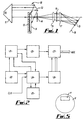
- Fig. 1 shows diagrammatically colour measurement apparatus 10 for measuring the colour of a gambling chip X.
- Apparatus according to the applicant's co-pending International Patent Application No. WO 96/23281 could be used in a method according to the present invention, and the apparatus of fig. 1 could be incorporated in a device for sorting gambling chips as described in this prior specification.
- the apparatus 10 comprises an illuminating halogen lamp 11 provided with a reflector.
- the lamp 11 faces a downwardly inclined mirror 12 for shining light downwardly onto a gambling chip X held in a chip holder 13.
- An inlet slit 14 is provided on the far side of the chip X from the lamp 11 for focusing a beam of light from the chip X.
- Light passing through the slit 14 strikes a collimator lens 15 which transforms the diverging beam of light from the slit 14 into a parallel beam.
- a no change parallel beam subsequently reaches a diffraction grating 16 which deflects the light of different wavelengths in different angles dependent on the wavelength.
- the deflected light passes to a focusing lens 17 to focus the parallel beams onto a focal surface 18 in which is installed an optical receiver 19.
- the optical receiver is an integrated optical sensor consisting of 64 charge mode pixels arranged in a 64 x 1 linear array provided with an internal logic circuit.
- the sensor 19 is located in a position to receive the spectra of the first order and the violet portion of the spectra of the second order, thereby allowing higher accuracy definition of the chip colour.
- Fig. 2 shows a functional diagram of an ADC (analog-digital converter).
- 21 is the optical receiver, reference number 19 in fig. 1; 22 is a signal generator; 23 is an adjustable amplifier; 24 is a start control circuit; 25 is a timer; 26 is an integrators control circuit; and 27 are eight integrators.
- SI is the serial input of the optical receiver 21, whilst S0 is the serial output of the receiver 21.
- A0 is the analog output t int is the integrated time of the receiver 21.
- RS is the read pulse signal.
- the converter circuit (fig. 2) controls the functioning of the optical receiver 21, and converts the output signal therefrom.
- the clock pulse signals from the generator 22 are fed to the clock (CLK) input of the optical receiver 21.
- the timer 25 determines the integration time t int of the receiver 21. During t int , information on the spectrum from the chip X is accumulated. Subsequently the timer 25 sends the read pulse signal RS which passes through the circuit 24 and is applied to the SI triggering the retrieval and accumulation of information concerning a spectra of the chip X.
- the analog signal from AO proportional to the integral spectrum of the scattered light of the chip passes via the amplifier 23 and is applied to the eight integrators 27.
- the pulse RS from the timer 25 is delivered to the integrators control circuit 26 and the receiver 21.
- the circuit 26 applies the signal from the receiver 21 in consecutive order to each of the integrators 27.
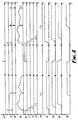
- On arrival of the control pulse signal C1 (fig. 4) data from the first to eighth pixels of the receiver 21 are integrated in the first integrator N1 (fig. 4).
- Data from the nineth to sixteenth pixels of the receiver 21 are integrated in the second integrator N2 upon arrival of the signal C2 and so on.
- data from the fifty sixth to sixty fourth pixels of the receiver 21 are integrated in N8.
- the information stored in all eight integrators until the arrival of the next signal CLK, following which the circuit 26 generates a reset signal (SET-fig. 4).
- the integrators 27 are reset and cleared of information before the arrival of the signal RS from the timer 25.
- the cycle of the next analog signal of the receiver 21 proceeds to its completion in a similar manner as shown on the second half of the diagram in fig. 4.
- the signal SO from the receiver 21 which is generated after the retrieval and partial erasure of the information passes through the circuit controlling the receiver 21 and is applied to the input SI thereof.
- the readout and partial erasure of the remaining information in the receiver 21 is effected again.
- the signal SO is again delivered to the SI input and so on. A complete erasure of the accumulated information will take place before the arrival of the next clock pulse signal.
- the spectral composition of the scattered light from the chip X from an area measuring approximately 1 x 3 mm is measured each time.
- the colour of the chip X is measured fifteen times such that the integrated spectrum of the chip X is obtained from an area Y of the chip X measuring 3 x 15 mm (fig. 5).
- This arrangement of measuring the colour of the chip at a number of locations, in this instance fifteen, across the chip and integrating the results obtained provides for an increased accuracy of colour measurement. This arrangement also helps to reduce the effect of spurious colour results due perhaps to particular colour abberations or dirt on the chip.
- the apparatus would first be set by recording the colours of required test chips. Usually a number of different coloured test chips would be measured by a method as described above. Normally a number of each colour of test chip would be measured and/or each chip may be measured a number of times. Each test chip would be allocated to a particular location in the sorting device, and chips subsequently measured which correspond to one of the test chips would automatically be directed to the required location.
Landscapes
- Physics & Mathematics (AREA)
- Spectroscopy & Molecular Physics (AREA)
- General Physics & Mathematics (AREA)
- Spectrometry And Color Measurement (AREA)
- Sorting Of Articles (AREA)
- Manufacture, Treatment Of Glass Fibers (AREA)
- Investigating Or Analysing Materials By The Use Of Chemical Reactions (AREA)
- Investigating Or Analysing Materials By Optical Means (AREA)
Applications Claiming Priority (3)
| Application Number | Priority Date | Filing Date | Title |
|---|---|---|---|
| GB9508632 | 1995-04-28 | ||
| GBGB9508632.8A GB9508632D0 (en) | 1995-04-28 | 1995-04-28 | Colour detection method |
| PCT/GB1996/000969 WO1996034258A1 (en) | 1995-04-28 | 1996-04-24 | Colour detection method |
Publications (2)
| Publication Number | Publication Date |
|---|---|
| EP0823041A1 EP0823041A1 (en) | 1998-02-11 |
| EP0823041B1 true EP0823041B1 (en) | 2002-09-04 |
Family
ID=10773662
Family Applications (1)
| Application Number | Title | Priority Date | Filing Date |
|---|---|---|---|
| EP96910142A Expired - Lifetime EP0823041B1 (en) | 1995-04-28 | 1996-04-24 | Colour detection method |
Country Status (11)
| Country | Link |
|---|---|
| US (1) | US5933244A (da) |
| EP (1) | EP0823041B1 (da) |
| AT (1) | ATE223571T1 (da) |
| AU (1) | AU698843B2 (da) |
| CA (1) | CA2229053C (da) |
| DE (1) | DE69623457T2 (da) |
| DK (1) | DK0823041T3 (da) |
| ES (1) | ES2178706T3 (da) |
| GB (1) | GB9508632D0 (da) |
| NZ (1) | NZ305450A (da) |
| WO (1) | WO1996034258A1 (da) |
Cited By (5)
| Publication number | Priority date | Publication date | Assignee | Title |
|---|---|---|---|---|
| US8298052B2 (en) | 2003-02-03 | 2012-10-30 | Shuffle Master Gmbh & Co Kg | Apparatus for sorting articles |
| US8336699B2 (en) | 2009-11-02 | 2012-12-25 | Shuffle Master Gmbh & Co Kg | Chip sorting devices, components therefor and methods of ejecting chips |
| US8393942B2 (en) | 2002-06-05 | 2013-03-12 | Shuffle Master Gmbh & Co Kg | Methods for displacing chips in a chip stack |
| US10096192B1 (en) | 2017-08-30 | 2018-10-09 | Shuffle Master Gmbh & Co Kg | Chip sorting devices and related assemblies and methods |
| US10255741B2 (en) | 2016-04-06 | 2019-04-09 | Shuffle Master Gmbh & Co Kg | Chip sorting devices and related assemblies, components and methods |
Families Citing this family (24)
| Publication number | Priority date | Publication date | Assignee | Title |
|---|---|---|---|---|
| SE523567C2 (sv) * | 1999-01-08 | 2004-04-27 | Scan Coin Ind Ab | Myntsärskiljande anordning och metod |
| DE19920184C2 (de) * | 1999-05-03 | 2001-06-07 | Optosens Optische Spektroskopi | Verfahren für die gleichzeitige Erfassung von diffuser und specularer Reflexion von Proben, insbesondere undurchsichtiger Proben, sowie Reflektanz-Meßsonde |
| US6567159B1 (en) * | 1999-10-13 | 2003-05-20 | Gaming Analysis, Inc. | System for recognizing a gaming chip and method of use |
| AT6405U1 (de) | 2002-06-05 | 2003-10-27 | Card Casinos Austria Res & Dev | Chipsortiervorrichtung |
| US20060063586A1 (en) * | 2004-09-23 | 2006-03-23 | Shuffle Master, Inc. | Electronic value marking for wagering chips |
| US20060068878A1 (en) * | 2004-09-29 | 2006-03-30 | Shuffle Master Gmbh & Co Kg | Roulette revenue method and apparatus |
| US8081304B2 (en) | 2006-07-31 | 2011-12-20 | Visualant, Inc. | Method, apparatus, and article to facilitate evaluation of objects using electromagnetic energy |
| WO2008016590A2 (en) | 2006-07-31 | 2008-02-07 | Visualant, Inc. | System and method of evaluating an object using electromagnetic energy |
| US7996173B2 (en) * | 2006-07-31 | 2011-08-09 | Visualant, Inc. | Method, apparatus, and article to facilitate distributed evaluation of objects using electromagnetic energy |
| USD692066S1 (en) | 2011-08-08 | 2013-10-22 | Tech Art, Inc. | Chip rack with integrated hole card reader |
| USD692068S1 (en) | 2011-08-12 | 2013-10-22 | Tech Art, Inc. | Modified chip rack with integrated hole card reader |
| USD692067S1 (en) | 2011-08-08 | 2013-10-22 | Tech Art, Inc. | Chip rack with integrated hole card reader |
| USD839965S1 (en) | 2011-08-08 | 2019-02-05 | Bally Gaming, Inc. | Chip racks |
| USD680537S1 (en) | 2011-08-08 | 2013-04-23 | Tech Art, Inc. | Hole card reader |
| US8567784B2 (en) | 2011-08-08 | 2013-10-29 | Tech Art, Inc. | Integrated blackjack hole card readers and chip racks, and improved covers for chip racks |
| USD686208S1 (en) | 2011-08-26 | 2013-07-16 | Tech Art, Inc. | Modified hole card reader |
| USD687435S1 (en) | 2011-08-26 | 2013-08-06 | Tech Art, Inc. | Arched hole card reader |
| USD687829S1 (en) | 2011-08-26 | 2013-08-13 | Tech Art, Inc. | Triangular shaped playing card reader |
| USD688241S1 (en) | 2011-08-26 | 2013-08-20 | Tech Art, Inc. | Square shaped playing card reader |
| USD705364S1 (en) | 2011-09-14 | 2014-05-20 | Tech Art, Inc. | Oval hole card reader |
| US8888207B2 (en) | 2012-02-10 | 2014-11-18 | Visualant, Inc. | Systems, methods and articles related to machine-readable indicia and symbols |
| US9316581B2 (en) | 2013-02-04 | 2016-04-19 | Visualant, Inc. | Method, apparatus, and article to facilitate evaluation of substances using electromagnetic energy |
| US9041920B2 (en) | 2013-02-21 | 2015-05-26 | Visualant, Inc. | Device for evaluation of fluids using electromagnetic energy |
| WO2014165003A1 (en) | 2013-03-12 | 2014-10-09 | Visualant, Inc. | Systems and methods for fluid analysis using electromagnetic energy |
Family Cites Families (7)
| Publication number | Priority date | Publication date | Assignee | Title |
|---|---|---|---|---|
| US2022327A (en) * | 1932-06-28 | 1935-11-26 | Sheldon Electric Corp | Apparatus for the comparison of colors |
| US4707138A (en) * | 1985-06-03 | 1987-11-17 | Filper Industries, Inc. | Color measuring and control device |
| US4841140A (en) * | 1987-11-09 | 1989-06-20 | Honeywell Inc. | Real-time color comparator |
| US4954972A (en) * | 1987-11-09 | 1990-09-04 | Honeywell Inc. | Color signature sensor |
| DK163837C (da) * | 1987-11-10 | 1994-09-05 | Neltec As | Apparat til farvekontrol af genstande |
| JPH04332830A (ja) * | 1991-05-08 | 1992-11-19 | Takayama:Kk | 光検出装置 |
| US5374988A (en) * | 1991-06-14 | 1994-12-20 | Ball Corporation | System for non-contact identification and inspection of color patterns |
-
1995
- 1995-04-28 GB GBGB9508632.8A patent/GB9508632D0/en active Pending
-
1996
- 1996-04-24 DE DE69623457T patent/DE69623457T2/de not_active Expired - Fee Related
- 1996-04-24 WO PCT/GB1996/000969 patent/WO1996034258A1/en not_active Ceased
- 1996-04-24 NZ NZ305450A patent/NZ305450A/en unknown
- 1996-04-24 DK DK96910142T patent/DK0823041T3/da active
- 1996-04-24 US US08/945,615 patent/US5933244A/en not_active Expired - Fee Related
- 1996-04-24 EP EP96910142A patent/EP0823041B1/en not_active Expired - Lifetime
- 1996-04-24 ES ES96910142T patent/ES2178706T3/es not_active Expired - Lifetime
- 1996-04-24 AU AU53440/96A patent/AU698843B2/en not_active Ceased
- 1996-04-24 AT AT96910142T patent/ATE223571T1/de not_active IP Right Cessation
- 1996-04-24 CA CA002229053A patent/CA2229053C/en not_active Expired - Fee Related
Cited By (12)
| Publication number | Priority date | Publication date | Assignee | Title |
|---|---|---|---|---|
| US8393942B2 (en) | 2002-06-05 | 2013-03-12 | Shuffle Master Gmbh & Co Kg | Methods for displacing chips in a chip stack |
| US8298052B2 (en) | 2003-02-03 | 2012-10-30 | Shuffle Master Gmbh & Co Kg | Apparatus for sorting articles |
| US8678164B2 (en) | 2003-02-03 | 2014-03-25 | Shuffle Master Gmbh & Co Kg | Apparatus for receiving and sorting disks |
| US9330516B2 (en) | 2003-02-03 | 2016-05-03 | Shuffle Master Gmbh & Co Kg | Apparatus for receiving and sorting disks |
| US9589407B2 (en) | 2003-02-03 | 2017-03-07 | Shuffle Master Gmbh & Co Kg | Apparatus for receiving and sorting disks |
| US9990792B2 (en) | 2003-02-03 | 2018-06-05 | Shuffle Master Gmbh & Co Kg | Methods and apparatus for receiving and sorting disks |
| US10706656B2 (en) | 2003-02-03 | 2020-07-07 | Shuffle Master Gmbh & Co Kg | Methods and apparatus for receiving and sorting disks |
| US8336699B2 (en) | 2009-11-02 | 2012-12-25 | Shuffle Master Gmbh & Co Kg | Chip sorting devices, components therefor and methods of ejecting chips |
| US8757349B2 (en) | 2009-11-02 | 2014-06-24 | Shuffle Master Gmbh & Co Kg | Methods of ejecting chips |
| US9384616B2 (en) | 2009-11-02 | 2016-07-05 | Shuffle Master Gmbh & Co Kg | Chip handling devices and related methods |
| US10255741B2 (en) | 2016-04-06 | 2019-04-09 | Shuffle Master Gmbh & Co Kg | Chip sorting devices and related assemblies, components and methods |
| US10096192B1 (en) | 2017-08-30 | 2018-10-09 | Shuffle Master Gmbh & Co Kg | Chip sorting devices and related assemblies and methods |
Also Published As
| Publication number | Publication date |
|---|---|
| DE69623457T2 (de) | 2003-01-16 |
| US5933244A (en) | 1999-08-03 |
| ES2178706T3 (es) | 2003-01-01 |
| DK0823041T3 (da) | 2002-10-28 |
| CA2229053C (en) | 2006-11-14 |
| AU698843B2 (en) | 1998-11-12 |
| AU5344096A (en) | 1996-11-18 |
| CA2229053A1 (en) | 1996-10-31 |
| WO1996034258A1 (en) | 1996-10-31 |
| ATE223571T1 (de) | 2002-09-15 |
| NZ305450A (en) | 1999-04-29 |
| GB9508632D0 (en) | 1995-06-14 |
| EP0823041A1 (en) | 1998-02-11 |
| DE69623457D1 (de) | 2002-10-10 |
Similar Documents
| Publication | Publication Date | Title |
|---|---|---|
| EP0823041B1 (en) | Colour detection method | |
| US5793486A (en) | Dual spectrometer color sensor | |
| US4076421A (en) | Spectrophotometer with parallel sensing | |
| US5072128A (en) | Defect inspecting apparatus using multiple color light to detect defects | |
| JP4377107B2 (ja) | 反射体の特性を決定する装置及びその方法 | |
| AU608807B2 (en) | Apparatus for monitoring bloodstream | |
| CA1276809C (en) | Producing signals responsive to a parameter of successive objects | |
| US4186838A (en) | Measurement of optical properties | |
| RU2170420C2 (ru) | Устройство и способ детектирования флуоресцентного и фосфоресцентного свечения | |
| US5367379A (en) | Luster detector | |
| IE852733L (en) | Improved color sensor | |
| KR970066557A (ko) | 적외선 수분 측정장치 및 적외선 수분 측정방법 | |
| EP0806020B1 (en) | Colour detection apparatus | |
| JPH0688745A (ja) | 光検出器の直線性決定方法および精密測光機器 | |
| GB2123139A (en) | A device for the fast measurement of the gloss of a surface | |
| JPH0369057B2 (da) | ||
| SU364877A1 (ru) | Анализатор дисперсности гетерогенных систем | |
| US4792679A (en) | Apparatus for incremental length measurement having an inclined slot over the light source | |
| US6411380B1 (en) | Detection device for a spectrophotometer | |
| JP2005265849A (ja) | 光センサ及び入射光を検知する方法 | |
| SU1711001A1 (ru) | Устройство дл контрол шероховатости поверхности | |
| US20040164233A1 (en) | Colour sensing apparatus and method | |
| JPH03279823A (ja) | プラズマ発光分光装置 | |
| JPS61251749A (ja) | 紙の光学的特性測定装置 |
Legal Events
| Date | Code | Title | Description |
|---|---|---|---|
| PUAI | Public reference made under article 153(3) epc to a published international application that has entered the european phase |
Free format text: ORIGINAL CODE: 0009012 |
|
| 17P | Request for examination filed |
Effective date: 19971118 |
|
| AK | Designated contracting states |
Kind code of ref document: A1 Designated state(s): AT DE DK ES FR GB GR IE IT MC SE |
|
| 17Q | First examination report despatched |
Effective date: 19991124 |
|
| GRAG | Despatch of communication of intention to grant |
Free format text: ORIGINAL CODE: EPIDOS AGRA |
|
| GRAG | Despatch of communication of intention to grant |
Free format text: ORIGINAL CODE: EPIDOS AGRA |
|
| GRAH | Despatch of communication of intention to grant a patent |
Free format text: ORIGINAL CODE: EPIDOS IGRA |
|
| GRAH | Despatch of communication of intention to grant a patent |
Free format text: ORIGINAL CODE: EPIDOS IGRA |
|
| RAP1 | Party data changed (applicant data changed or rights of an application transferred) |
Owner name: TECHNICAL CASINO SERVICES LIMITED |
|
| GRAA | (expected) grant |
Free format text: ORIGINAL CODE: 0009210 |
|
| AK | Designated contracting states |
Kind code of ref document: B1 Designated state(s): AT DE DK ES FR GB GR IE IT MC SE |
|
| REF | Corresponds to: |
Ref document number: 223571 Country of ref document: AT Date of ref document: 20020915 Kind code of ref document: T |
|
| REG | Reference to a national code |
Ref country code: GB Ref legal event code: FG4D |
|
| REG | Reference to a national code |
Ref country code: IE Ref legal event code: FG4D |
|
| REF | Corresponds to: |
Ref document number: 69623457 Country of ref document: DE Date of ref document: 20021010 |
|
| REG | Reference to a national code |
Ref country code: DK Ref legal event code: T3 |
|
| REG | Reference to a national code |
Ref country code: GR Ref legal event code: EP Ref document number: 20020403266 Country of ref document: GR |
|
| REG | Reference to a national code |
Ref country code: ES Ref legal event code: FG2A Ref document number: 2178706 Country of ref document: ES Kind code of ref document: T3 |
|
| ET | Fr: translation filed | ||
| PLBE | No opposition filed within time limit |
Free format text: ORIGINAL CODE: 0009261 |
|
| STAA | Information on the status of an ep patent application or granted ep patent |
Free format text: STATUS: NO OPPOSITION FILED WITHIN TIME LIMIT |
|
| 26N | No opposition filed |
Effective date: 20030605 |
|
| PGFP | Annual fee paid to national office [announced via postgrant information from national office to epo] |
Ref country code: MC Payment date: 20080331 Year of fee payment: 13 |
|
| PGFP | Annual fee paid to national office [announced via postgrant information from national office to epo] |
Ref country code: ES Payment date: 20080401 Year of fee payment: 13 Ref country code: DK Payment date: 20080425 Year of fee payment: 13 |
|
| PGFP | Annual fee paid to national office [announced via postgrant information from national office to epo] |
Ref country code: IT Payment date: 20080422 Year of fee payment: 13 |
|
| PGFP | Annual fee paid to national office [announced via postgrant information from national office to epo] |
Ref country code: SE Payment date: 20080414 Year of fee payment: 13 Ref country code: IE Payment date: 20080407 Year of fee payment: 13 Ref country code: DE Payment date: 20080624 Year of fee payment: 13 |
|
| PGFP | Annual fee paid to national office [announced via postgrant information from national office to epo] |
Ref country code: FR Payment date: 20080404 Year of fee payment: 13 |
|
| PGFP | Annual fee paid to national office [announced via postgrant information from national office to epo] |
Ref country code: GR Payment date: 20080430 Year of fee payment: 13 |
|
| PGFP | Annual fee paid to national office [announced via postgrant information from national office to epo] |
Ref country code: GB Payment date: 20090430 Year of fee payment: 14 |
|
| REG | Reference to a national code |
Ref country code: DK Ref legal event code: EBP |
|
| EUG | Se: european patent has lapsed | ||
| REG | Reference to a national code |
Ref country code: FR Ref legal event code: ST Effective date: 20091231 |
|
| PG25 | Lapsed in a contracting state [announced via postgrant information from national office to epo] |
Ref country code: DE Free format text: LAPSE BECAUSE OF NON-PAYMENT OF DUE FEES Effective date: 20091103 |
|
| REG | Reference to a national code |
Ref country code: IE Ref legal event code: MM4A |
|
| PG25 | Lapsed in a contracting state [announced via postgrant information from national office to epo] |
Ref country code: MC Free format text: LAPSE BECAUSE OF NON-PAYMENT OF DUE FEES Effective date: 20090430 Ref country code: IE Free format text: LAPSE BECAUSE OF NON-PAYMENT OF DUE FEES Effective date: 20090424 Ref country code: FR Free format text: LAPSE BECAUSE OF NON-PAYMENT OF DUE FEES Effective date: 20091222 Ref country code: DK Free format text: LAPSE BECAUSE OF NON-PAYMENT OF DUE FEES Effective date: 20090430 |
|
| REG | Reference to a national code |
Ref country code: ES Ref legal event code: FD2A Effective date: 20090425 |
|
| PG25 | Lapsed in a contracting state [announced via postgrant information from national office to epo] |
Ref country code: GR Free format text: LAPSE BECAUSE OF NON-PAYMENT OF DUE FEES Effective date: 20091104 |
|
| PG25 | Lapsed in a contracting state [announced via postgrant information from national office to epo] |
Ref country code: ES Free format text: LAPSE BECAUSE OF NON-PAYMENT OF DUE FEES Effective date: 20090425 |
|
| PGFP | Annual fee paid to national office [announced via postgrant information from national office to epo] |
Ref country code: AT Payment date: 20100426 Year of fee payment: 15 |
|
| GBPC | Gb: european patent ceased through non-payment of renewal fee |
Effective date: 20100424 |
|
| PG25 | Lapsed in a contracting state [announced via postgrant information from national office to epo] |
Ref country code: IT Free format text: LAPSE BECAUSE OF NON-PAYMENT OF DUE FEES Effective date: 20090424 Ref country code: GB Free format text: LAPSE BECAUSE OF NON-PAYMENT OF DUE FEES Effective date: 20100424 |
|
| PG25 | Lapsed in a contracting state [announced via postgrant information from national office to epo] |
Ref country code: SE Free format text: LAPSE BECAUSE OF NON-PAYMENT OF DUE FEES Effective date: 20090425 |
|
| REG | Reference to a national code |
Ref country code: AT Ref legal event code: MM01 Ref document number: 223571 Country of ref document: AT Kind code of ref document: T Effective date: 20110424 |
|
| PG25 | Lapsed in a contracting state [announced via postgrant information from national office to epo] |
Ref country code: AT Free format text: LAPSE BECAUSE OF NON-PAYMENT OF DUE FEES Effective date: 20110424 |