EP0821844B1 - Method for processing pwm waves and devices therefor - Google Patents
Method for processing pwm waves and devices therefor Download PDFInfo
- Publication number
- EP0821844B1 EP0821844B1 EP96908936A EP96908936A EP0821844B1 EP 0821844 B1 EP0821844 B1 EP 0821844B1 EP 96908936 A EP96908936 A EP 96908936A EP 96908936 A EP96908936 A EP 96908936A EP 0821844 B1 EP0821844 B1 EP 0821844B1
- Authority
- EP
- European Patent Office
- Prior art keywords
- inverter
- current
- rectifier
- voltage
- corrected
- Prior art date
- Legal status (The legal status is an assumption and is not a legal conclusion. Google has not performed a legal analysis and makes no representation as to the accuracy of the status listed.)
- Expired - Lifetime
Links
Images


Classifications
-
- H—ELECTRICITY
- H02—GENERATION; CONVERSION OR DISTRIBUTION OF ELECTRIC POWER
- H02M—APPARATUS FOR CONVERSION BETWEEN AC AND AC, BETWEEN AC AND DC, OR BETWEEN DC AND DC, AND FOR USE WITH MAINS OR SIMILAR POWER SUPPLY SYSTEMS; CONVERSION OF DC OR AC INPUT POWER INTO SURGE OUTPUT POWER; CONTROL OR REGULATION THEREOF
- H02M1/00—Details of apparatus for conversion
- H02M1/38—Means for preventing simultaneous conduction of switches
-
- H—ELECTRICITY
- H02—GENERATION; CONVERSION OR DISTRIBUTION OF ELECTRIC POWER
- H02M—APPARATUS FOR CONVERSION BETWEEN AC AND AC, BETWEEN AC AND DC, OR BETWEEN DC AND DC, AND FOR USE WITH MAINS OR SIMILAR POWER SUPPLY SYSTEMS; CONVERSION OF DC OR AC INPUT POWER INTO SURGE OUTPUT POWER; CONTROL OR REGULATION THEREOF
- H02M1/00—Details of apparatus for conversion
- H02M1/12—Arrangements for reducing harmonics from ac input or output
-
- H—ELECTRICITY
- H02—GENERATION; CONVERSION OR DISTRIBUTION OF ELECTRIC POWER
- H02M—APPARATUS FOR CONVERSION BETWEEN AC AND AC, BETWEEN AC AND DC, OR BETWEEN DC AND DC, AND FOR USE WITH MAINS OR SIMILAR POWER SUPPLY SYSTEMS; CONVERSION OF DC OR AC INPUT POWER INTO SURGE OUTPUT POWER; CONTROL OR REGULATION THEREOF
- H02M7/00—Conversion of ac power input into dc power output; Conversion of dc power input into ac power output
- H02M7/42—Conversion of dc power input into ac power output without possibility of reversal
- H02M7/44—Conversion of dc power input into ac power output without possibility of reversal by static converters
- H02M7/48—Conversion of dc power input into ac power output without possibility of reversal by static converters using discharge tubes with control electrode or semiconductor devices with control electrode
- H02M7/53—Conversion of dc power input into ac power output without possibility of reversal by static converters using discharge tubes with control electrode or semiconductor devices with control electrode using devices of a triode or transistor type requiring continuous application of a control signal
- H02M7/537—Conversion of dc power input into ac power output without possibility of reversal by static converters using discharge tubes with control electrode or semiconductor devices with control electrode using devices of a triode or transistor type requiring continuous application of a control signal using semiconductor devices only, e.g. single switched pulse inverters
- H02M7/539—Conversion of dc power input into ac power output without possibility of reversal by static converters using discharge tubes with control electrode or semiconductor devices with control electrode using devices of a triode or transistor type requiring continuous application of a control signal using semiconductor devices only, e.g. single switched pulse inverters with automatic control of output wave form or frequency
- H02M7/5395—Conversion of dc power input into ac power output without possibility of reversal by static converters using discharge tubes with control electrode or semiconductor devices with control electrode using devices of a triode or transistor type requiring continuous application of a control signal using semiconductor devices only, e.g. single switched pulse inverters with automatic control of output wave form or frequency by pulse-width modulation
Definitions
- the present invention relates to a method of processing of PWM waves intended for an inverter or a controlled rectifier, and more particularly in view obtain the reduction of harmonics.
- the present invention also relates to devices for implementing the method according to the present invention.
- the inverters and more particularly the voltage inverters, are intended to supply a voltage alternative from a DC voltage, while the controlled rectifiers are intended to supply voltage continues from an AC voltage.
- inverters can be used for variable speed control of machines synchronous or asynchronous.
- Voltage inverters are good devices known which generally use assemblies of components such as thyristors, GTOs, ... which switch particularly quickly.
- An inverter is controlled by a modulator and a discriminator.
- the role of the modulator is to create a wave setpoint, while the discriminator allows to separate this wave in several waves intended for the command individual switches.
- the simplest inverters are on two levels and consist of two switches (thyristors, GTO, ...) which supply the load alternately.
- This charge being of selfic type, it is necessary that a diode called “freewheeling diode” is placed in parallel on each switch to allow the charging current to circulate when the corresponding switch is open.
- harmonic 6 which is the most troublesome harmonic, because for a motor powered by 1/6 of the frequency used for signaling, there will be risk of interference. For example, a powered motor at 8 1/3 Hz may cause disturbance in the signaling system which uses 50 Hz.
- Another problem is that different switches cannot switch instantly of a zero value (current flowing and corresponding to the closing) at a positive value of the voltage (zero current and corresponding to the opening) and vice versa. This means that for a certain period of time, we simultaneously have a non-zero voltage and non-zero current, and therefore observes a loss of power on each switching.
- a support unit for switching In order to solve this problem, in case the various components cannot withstand such loss of power, it is known to offer a support unit for switching.
- An example of such a cell can be constituted simply by a "snubber" which includes basically a capacity paralleled on each switch. This snubber aims to absorb the losses of power by limiting the voltage, and more particularly by limiting its growth, when switching.
- Another example of a cell often used in combination with the snubber is the cell called "di / dt", which includes essentially a choke in series with the switches.
- GB-2 238 188 describes a converter controlled by a PWM generator and which has a reference signal generator (setpoint) associated with a zero current level detected by a outgoing current to give a signal to the PWM generator.
- a control is provided to avoid a short circuit between the controllable elements used as switches in the PWM converter which generates an alternating voltage variable or alternating current indicative of a variable frequency.
- a selector chooses an output in the period during which the result of detection by the current detector falls in the region of a zero level substantial by selecting a corresponding signal for each switch which actually acts on the output current production, outside signals generated by a PWM signal generator during a period other than that described above, and producing thus the equivalent of a control signal for the switch.
- the current detector is used to determine the polarity of the output and the control ensured the fact that only the switches generating the output of correct polarity can be ordered.
- the present invention aims to propose a method which makes it possible to reduce, until canceling, the effect of the times dead in a controlled inverter or rectifier, and allows therefore reduce the effect of unwanted harmonics.
- the present invention aims in particular to propose a process that can be applied to inverters or controlled rectifiers, with or without switching, whether two-level or multi-level.
- the present invention aims to propose in the case of a three-phase inverter supplying a synchronous or asynchronous motor, a process which allows reduce unwanted harmonics such as harmonics 5 and 7 appearing in the motor currents, and therefore the harmonic 6 appearing on the supply side and engine torque side.
- the present invention relates to a method for processing PWM waves intended to control a voltage inverter or a voltage rectifier, this inverter or rectifier comprising at least a branch with at least one pair of switches connected in series, by which a modulator creates the PWM control wave in the form of a succession of high and low states, the high state being defined by the fact that the switch connected to the most positive voltage is closed while the switch connected to the most negative voltage is open, and the low state being defined by the reverse, characterized in that the PWM control wave is corrected according to the direction of the current leaving or entering the branch so as to obtain two corrected setpoints, the corrected setpoint for the outgoing current having a high state increased by a delay during the transition from the high state to the low state, and the corrected setpoint for the inrush current t having a low state increased by a delay during the transition from the low state to the high state.
- the corrected instructions introduce deadlines which correspond to the dead time created itself by the discriminator.
- delay introduced in the corrected instructions depends not only of the direction of the current, but also of its value.
- the present invention also relates to a device for implementation of the PWM wave treatment method according to the invention and which are intended to control a voltage inverter or a voltage rectifier, the inverter or rectifier comprising at least one branch with at least one pair of switches connected in series, the device comprising a modulator creating the PWM control wave in the form of a succession of high and low states, the state high being defined by the fact that the switch connected to the most positive voltage is closed while the switch connected to the most negative voltage is open, and the low state being defined by the reverse, characterized in that means of correction correct the PWM control wave according to the direction of the current entering or leaving the branch of the inverter, so as to create two setpoints, a corrected setpoint for the outgoing current having a high increased state of a delay during the transition from the high state to the low state, and a corrected setpoint for the incoming current having a low state increased by a delay during the transition from the low state to the high state .
- FIG. 1 shows schematically a branch of a conventional two-level inverter and that is used in the context of the present invention.
- this inverter includes two switches S1 and S2 which alternately supply a load which can be by example a phase of an asynchronous motor.
- charge is of the selfic type and it is necessary that each of the two switches S1 and S2 is mounted in parallel with a diode called “freewheeling diode" DR1 or DR2 which allows the charging current to flow when the corresponding switch is open.
- DR1 or DR2 freewheeling diode
- the presence of this diode allows the inductive load current to decrease and thus avoid any destructive overvoltage when the corresponding switch is open.
- the inverter is controlled by a modulator and a discriminator.
- a setpoint wave M is shown which is in the form of successive slots.
- the switch S1 When reaching the high level 1, this means that the switch S1 must be closed and that the switch S2 must be open. Conversely, when the low level 2 is reached, the switch S2 must be closed while the switch S1 must be open. Consequently, on each rising or falling edge, the switch S1 should be instantly switched to close it and the switch S2 to open or vice versa.
- Figures 2b and 2c show the waves modified by the discriminator and which will control the two switches S1 and S2.
- the closing a switch making the branch conductive does is done more instantaneously, but is done with a delay called "dead time", while the opening leading at cut-off can be considered instantaneous.
- the present invention aims to propose a solution to this problem by suggesting to use two corrected commands, one for the case where the current is outgoing and the other for the case where the current is incoming.
- Figure 3 shows a block diagram of a device for controlling a conventional inverter at two levels using the method according to the present invention.
- the discriminator is either ordered by a corrected setpoint for outgoing current, either by a corrected setpoint for incoming current. This is the meaning of current in the load which will determine if we use one either of the two corrected instructions.
- FIG. 4 represents the ideal setpoint wave M (fig. 4a) and each of the two corrected setpoints, on the one hand for the outgoing current (fig. 4b) and on the other hand for the incoming current (fig. 4c).
- the high level 1 is increased by a time T m corresponding in this case to the dead time on the falling edge, that is to say say during a transition from the high state 1 to the low state 2.
- This transition actually corresponds to the opening of the switch S1 and the closing of the switch S2.
- the corrected setpoint for the incoming current has a high level 1 reduced by a time T m also corresponding to the dead time at each rising edge, that is to say during the transition from the low state 2 to the state top 1.
- FIGS. 4d and 4e also show the output voltages in the case where corrected setpoints are used, either for incoming current or for outgoing current. It is observed that the correction makes it possible to make the output voltage of the inverter identical in both cases and identical to what it would be without dead time except for a delay T m .
- Figure 5 shows a schematic view of a branch of a conventional two-level inverter with snubber.
- This snubber is actually a support cell for switching, which absorbs power losses which appear with each switching of switches S1 and S2 by limiting the tension, and more particularly by limiting its growth.
- this cell includes a capacity C1 (or C2) placed in parallel on each switch, this capacity being itself in series with a resistor R1 (or R2) and a second diode D1 (or D2) which is opposite to that of the wheel diode free DR1 (or DR2).
- Figure 6 shows the setpoint wave M (fig. 6a) as well as the corresponding voltages applied to the motor in the case of a low incoming current (fig. 6b), in the case of a high incoming current (fig. 6c ), in the case of a weak outgoing current (fig. 6d) and in the case of a high outgoing current (fig. 6e).
- the freewheeling diode upper DR1 conducts and lets the current flow to food (fig. 6g).
- the corrected instruction should present, depending on whether it is an outgoing current or incoming, level 1 increased or decreased by one time corresponding to a time called "effective time" which would take into account the value of the current.
- T eff T dead
- FIGS. 7 also shows the pace general of the motor currents either in the case where does not apply the method according to the present invention (fig. 7a), either in the case where this process is applied (fig. 7b), for an inverter without snubber.
- FIGS. 8 show the harmonics 5 and 7 on the current side as well as the harmonic 6 on the power supply side, on the one hand in the case where the process is not applied according to the present invention (see figs. 8a and 8b) and other part in the case where this process is applied (figs. 8c and 8d).
Abstract
Description
La présente invention concerne un procédé de traitement d'ondes PWM destinées à un onduleur ou à un redresseur commandé, et plus particulièrement en vue d'obtenir la réduction d'harmoniques.The present invention relates to a method of processing of PWM waves intended for an inverter or a controlled rectifier, and more particularly in view obtain the reduction of harmonics.
La présente invention se rapporte également aux dispositifs pour la mise en oeuvre du procédé selon la présente invention.The present invention also relates to devices for implementing the method according to the present invention.
Les onduleurs, et plus particulièrement les onduleurs de tension, sont destinés à fournir une tension alternative à partir d'une tension continue, tandis que les redresseurs commandés sont destinés à fournir une tension continue à partir d'une tension alternative.The inverters, and more particularly the voltage inverters, are intended to supply a voltage alternative from a DC voltage, while the controlled rectifiers are intended to supply voltage continues from an AC voltage.
Dans la description qui suit, on s'attache plus particulièrement à décrire les onduleurs, mais exactement les mêmes problèmes se posent pour les redresseurs commandés.In the following description, we focus more particularly to describe the inverters, but exactly the the same problems arise for controlled rectifiers.
A titre d'exemple, les onduleurs peuvent être utilisés pour la commande en vitesse variable de machines synchrones ou asynchrones. For example, inverters can be used for variable speed control of machines synchronous or asynchronous.
Dans ce cas, il est nécessaire de fournir à la charge, et plus particulièrement à chaque phase d'un moteur synchrone ou asynchrone, un système triphasé en tension le plus proche possible d'un système triphasé sinusoïdal équilibré variable en fréquence et en amplitude.In this case, it is necessary to provide the load, and more particularly at each phase of an engine synchronous or asynchronous, a three-phase system in voltage the as close as possible to a three-phase sinusoidal system balanced variable in frequency and amplitude.
Les onduleurs de tension sont des dispositifs bien connus qui utilisent généralement des montages de composants de puissance tels que des thyristors, des GTO, ..., qui commutent de façon particulièrement rapide.Voltage inverters are good devices known which generally use assemblies of components such as thyristors, GTOs, ... which switch particularly quickly.
Un onduleur est commandé par un modulateur et un discriminateur. Le rôle du modulateur est de créer une onde de consigne, tandis que le discriminateur permet de séparer cette onde en plusieurs ondes destinées à la commande individuelle des différents commutateurs.An inverter is controlled by a modulator and a discriminator. The role of the modulator is to create a wave setpoint, while the discriminator allows to separate this wave in several waves intended for the command individual switches.
Les onduleurs les plus simples sont à deux niveaux et se composent de deux commutateurs (thyristors, GTO, ...) qui alimentent alternativement la charge. Cette charge étant de type selfique, il est nécessaire qu'une diode appelée "diode de roue libre" soit placée en parallèle sur chaque commutateur afin de permettre au courant de charge de circuler lorsque le commutateur correspondant est ouvert.The simplest inverters are on two levels and consist of two switches (thyristors, GTO, ...) which supply the load alternately. This charge being of selfic type, it is necessary that a diode called "freewheeling diode" is placed in parallel on each switch to allow the charging current to circulate when the corresponding switch is open.
Habituellement, on utilise une simple onde carrée comme onde de consigne, pour permettre la commutation de l'un ou l'autre des commutateurs à chaque flanc de créneau. Cette onde carrée devrait commander successivement la fermeture de l'un ou l'autre des commutateurs et simultanément l'ouverture du commutateur opposé.Usually we use a simple square wave as setpoint wave, to allow switching of one either of the switches on each slot edge. This square wave should successively order the closing of either switch and simultaneously opening from the opposite switch.
Pour des raisons évidentes de court-circuit de l'alimentation, il est impératif de vérifier que deux commutateurs ne soient jamais simultanément fermés. C'est à ce niveau que l'on retrouve le rôle du discriminateur, qui a pour but d'introduire un retard à la fermeture des commutateurs correspondants, de telle sorte que l'on soit toujours assuré que lorsque la commande de fermeture d'un commutateur est donnée, le commutateur opposé est déjà ouvert.For obvious reasons of short circuit of power supply, it is imperative to verify that two switches are never closed simultaneously. It's at this level that we find the role of the discriminator, which aims to introduce a delay in closing corresponding switches, so that one is always assured that when the command to close a switch is given, the opposite switch is already open.
Ceci signifie qu'il subsiste toujours un léger délai appelé "temps mort" entre le moment où un commutateur est ouvert et le moment où le commutateur opposé est fermé, les deux opérations n'étant donc jamais simultanées.This means that there is always a slight delay called "dead time" between the time a switch is open and when the opposite switch is closed, the two operations are therefore never simultaneous.
Ceci est la cause de la présence d'harmoniques indésirables, et plus particulièrement d'harmoniques 5 et 7, qui apparaissent dans les courants moteur, ce qui génère la présence d'une harmonique 6 côté alimentation et côté couple moteur.This is the cause of the presence of harmonics undesirable, and more particularly of harmonics 5 and 7, which appear in the motor currents, which generates the presence of a 6 harmonic on the supply side and the torque side engine.
En réalité, c'est l'harmonique 6 qui est l'harmonique la plus gênante, car pour un moteur alimenté à 1/6 de la fréquence utilisée pour la signalisation, il y aura risque d'interférence. A titre d'exemple, un moteur alimenté à 8 1/3 Hz risque de provoquer une perturbation dans le système de signalisation qui utilise le 50 Hz.In reality, it is harmonic 6 which is the most troublesome harmonic, because for a motor powered by 1/6 of the frequency used for signaling, there will be risk of interference. For example, a powered motor at 8 1/3 Hz may cause disturbance in the signaling system which uses 50 Hz.
Un autre problème réside dans le fait que les différents commutateurs ne peuvent commuter instantanément d'une valeur nulle (courant passant et correspondant à la fermeture) à une valeur positive de la tension (courant nul et correspondant à l'ouverture) et vice versa. Ceci signifie que pendant un certain laps de temps, on a simultanément une tension non nulle et un courant non nul, et de ce fait, on observe une perte de puissance à chaque commutation.Another problem is that different switches cannot switch instantly of a zero value (current flowing and corresponding to the closing) at a positive value of the voltage (zero current and corresponding to the opening) and vice versa. This means that for a certain period of time, we simultaneously have a non-zero voltage and non-zero current, and therefore observes a loss of power on each switching.
Afin de résoudre ce problème, dans le cas où les divers composants ne peuvent supporter une telle perte de puissance, il est connu de proposer une cellule d'aide à la commutation. Un exemple d'une telle cellule peut être constitué simplement par un "snubber" qui comprend essentiellement une capacité mise en parallèle sur chaque commutateur. Ce snubber a pour but d'absorber les pertes de puissance en limitant la tension, et plus particulièrement en limitant sa croissance, lors de la commutation. Un autre exemple de cellule souvent utilisé en combinaison avec le snubber est la cellule dite "di/dt", qui comprend essentiellement une self en série avec les commutateurs. Du fait de la présence de ces différentes cellules d'aide à la commutation, on observe alors une croissance plus lente de la tension, ce qui permet de limiter les pertes de puissance lors de la commutation.In order to solve this problem, in case the various components cannot withstand such loss of power, it is known to offer a support unit for switching. An example of such a cell can be constituted simply by a "snubber" which includes basically a capacity paralleled on each switch. This snubber aims to absorb the losses of power by limiting the voltage, and more particularly by limiting its growth, when switching. Another example of a cell often used in combination with the snubber is the cell called "di / dt", which includes essentially a choke in series with the switches. Of made of the presence of these different cells of assistance to the switching, we then observe a slower growth of voltage, which helps limit power losses when switching.
Le problème de la présence d'harmoniques est essentiellement le même pour un onduleur avec ou sans cellule d'aide à la commutation. En particulier, on observe également dans le cas de l'utilisation d'un onduleur avec snubber la présence d'harmoniques 5 et 7 coté moteur ainsi que la présence de l'harmonique 6 côté alimentation et côté couple moteur.The problem of the presence of harmonics is essentially the same for an inverter with or without cell assistance with switching. In particular, we also observe in the case of using an inverter with snubber the presence of harmonics 5 and 7 on the motor side as well as the presence of harmonic 6 on supply side and torque side engine.
Il convient de noter que dans le cas de redresseurs commandés, exactement les mêmes problèmes se posent, à la différence près que la charge doit être considérée dans ce cas comme la source et l'alimentation comme étant la charge. It should be noted that in the case of rectifiers ordered, exactly the same problems arise, at the difference near that the load should be considered in this case as the source and the feed as the load.
Le document GB-2 238 188 décrit un convertisseur commandé par un générateur PWM et qui possède un générateur de signal de référence (consigne) associé à un niveau zéro de courant détecté par un détecteur de courant sortant pour donner un signal au générateur PWM. Un contrôle est prévu pour éviter un court-circuit entre les éléments commandables utilisés comme interrupteurs dans le convertisseur PWM qui génère une tension alternative variable ou un courant alternatif indicateur d'une fréquence variable. Un sélecteur choisit une sortie dans la période durant laquelle le résultat de la détection par le détecteur de courant tombe dans la région d'un niveau zéro substantiel en sélectionnant un signal correspondant pour chaque interrupteur qui agit effectivement sur le production du courant de sortie, en dehors des signaux générés par un générateur de signaux PWM pendant une période autre que celle décrite ci-dessus, et produisant ainsi l'équivalent d'un signal de commande pour l'interrupteur. Le détecteur de courant est utilisé pour déterminer la polarité de la sortie et le contrôle assuré le fait que seuls les interrupteurs générant la sortie de polarité correcte pourront être commandés. GB-2 238 188 describes a converter controlled by a PWM generator and which has a reference signal generator (setpoint) associated with a zero current level detected by a outgoing current to give a signal to the PWM generator. A control is provided to avoid a short circuit between the controllable elements used as switches in the PWM converter which generates an alternating voltage variable or alternating current indicative of a variable frequency. A selector chooses an output in the period during which the result of detection by the current detector falls in the region of a zero level substantial by selecting a corresponding signal for each switch which actually acts on the output current production, outside signals generated by a PWM signal generator during a period other than that described above, and producing thus the equivalent of a control signal for the switch. The current detector is used to determine the polarity of the output and the control ensured the fact that only the switches generating the output of correct polarity can be ordered.
La présente invention vise à proposer un procédé qui permette de réduire, jusqu'à annuler, l'effet des temps morts dans un onduleur ou un redresseur commandé, et permet donc de réduire l'effet des harmoniques indésirables.The present invention aims to propose a method which makes it possible to reduce, until canceling, the effect of the times dead in a controlled inverter or rectifier, and allows therefore reduce the effect of unwanted harmonics.
La présente invention vise en particulier à proposer un procédé qui puisse être appliqué aux onduleurs ou redresseurs commandés, avec ou sans cellule d'aide à la commutation, qu'ils soient à deux niveaux ou multi-niveaux. The present invention aims in particular to propose a process that can be applied to inverters or controlled rectifiers, with or without switching, whether two-level or multi-level.
En particulier, la présente invention vise à proposer dans le cas d'un onduleur triphasé alimentant un moteur synchrone ou asynchrone, un procédé qui permette de réduire les harmoniques indésirables telles que les harmoniques 5 et 7 apparaissant dans les courants moteur, et de ce fait l'harmonique 6 apparaissant côté alimentation et côté couple moteur. In particular, the present invention aims to propose in the case of a three-phase inverter supplying a synchronous or asynchronous motor, a process which allows reduce unwanted harmonics such as harmonics 5 and 7 appearing in the motor currents, and therefore the harmonic 6 appearing on the supply side and engine torque side.
La présente invention se rapporte à un procédé de traitement d'ondes PWM destinées à la commande d'un onduleur de tension ou d' un redresseur de tension, cet onduleur ou redresseur comprenant au moins une branche avec au moins une paire de commutateurs reliés en série, par lequel un modulateur crée l'onde de commande PWM sous la forme d'une succession d'états hauts et d'états bas, l'état haut étant défini par le fait que le commutateur relié à la tension la plus positive est fermé tandis que le commutateur relié à la tension la plus négative est ouvert, et l'état bas étant défini par l'inverse, caractérisé en ce que l'onde de commande PWM est corrigée en fonction du sens du courant sortant ou entrant dans la branche de manière à obtenir deux consignes corrigées, la consigne corrigée pour le courant sortant présentant un état haut augmenté d'un délai lors de la transition de l'état haut vers l'état bas, et la consigne corrigée pour le courant entrant présentant un état bas augmenté d'un délai lors de la transition de l'état bas vers l'état haut. The present invention relates to a method for processing PWM waves intended to control a voltage inverter or a voltage rectifier, this inverter or rectifier comprising at least a branch with at least one pair of switches connected in series, by which a modulator creates the PWM control wave in the form of a succession of high and low states, the high state being defined by the fact that the switch connected to the most positive voltage is closed while the switch connected to the most negative voltage is open, and the low state being defined by the reverse, characterized in that the PWM control wave is corrected according to the direction of the current leaving or entering the branch so as to obtain two corrected setpoints, the corrected setpoint for the outgoing current having a high state increased by a delay during the transition from the high state to the low state, and the corrected setpoint for the inrush current t having a low state increased by a delay during the transition from the low state to the high state.
Dans le cas où l'onduleur ou redresseur est exempt de cellule d'aide à la commutation, les consignes corrigées introduisent des délais qui correspondent au temps mort créé lui-même par le discriminateur.In case the inverter or rectifier is exempt of switching assistance unit, the corrected instructions introduce deadlines which correspond to the dead time created itself by the discriminator.
Dans le cas où il s'agit d'un onduleur ou redresseur avec cellule d'aide à la commutation, le délai introduit dans les consignes corrigées dépend non seulement du sens du courant, mais également de sa valeur. In case it is an inverter or rectifier with switching assistance cell, delay introduced in the corrected instructions depends not only of the direction of the current, but also of its value.
Il convient de noter que le présent procédé peut être appliqué aussi bien aux onduleurs ou redresseurs à deux niveaux qu'aux onduleurs ou redresseurs multi-niveaux. It should be noted that the present process can be applied to both inverters or rectifiers with two levels than multi-level inverters or rectifiers.
La présente invention se rapporte également à un dispositif pour la mise en oeuvre du procédé de traitement d'ondes PWM selon l'invention et qui sont destinées à la commande d'un onduleur de tension ou d' un redresseur de tension, l'onduleur ou redresseur comprenant au moins une branche avec au moins une paire de commutateurs reliés en série, le dispositif comprenant un modulateur créant l'onde de commande PWM sous la forme d'une succession d'états hauts et d'états bas, l'état haut étant défini par le fait que le commutateur relié à la tension la plus positive est fermé tandis que le commutateur relié à la tension la plus négative est ouvert, et l'état bas étant défini par l'inverse, caractérisé en ce que des moyens de correction corrigent l'onde de commande PWM en fonction du sens du courant entrant ou sortant dans la branche de l'onduleur, de manière à créer deux consignes, une consigne corrigée pour le courant sortant présentant un état haut augmenté d'un délai lors de la transition de l'état haut vers l'état bas, et une consigne corrigée pour le courant entrant présentant un état bas augmenté d'un délai lors de la transition de l'état bas vers l'état haut. The present invention also relates to a device for implementation of the PWM wave treatment method according to the invention and which are intended to control a voltage inverter or a voltage rectifier, the inverter or rectifier comprising at least one branch with at least one pair of switches connected in series, the device comprising a modulator creating the PWM control wave in the form of a succession of high and low states, the state high being defined by the fact that the switch connected to the most positive voltage is closed while the switch connected to the most negative voltage is open, and the low state being defined by the reverse, characterized in that means of correction correct the PWM control wave according to the direction of the current entering or leaving the branch of the inverter, so as to create two setpoints, a corrected setpoint for the outgoing current having a high increased state of a delay during the transition from the high state to the low state, and a corrected setpoint for the incoming current having a low state increased by a delay during the transition from the low state to the high state .
La présente invention sera décrite plus en détails à l'aide des figures qui suivent :
- La figure 1
- représente une vue schématisée d'une branche d'un onduleur conventionnel à deux niveaux.
- La figure 2
- représente l'onde consigne (fig. 2a) créée par le modulateur pour un onduleur tel que décrit à la figure 1, ainsi que les ondes obtenues à la sortie du discriminateur et destinées à commander directement les commutateurs (fig. 2b et 2c) et les tensions correspondantes appliquées dans ce cas au moteur (fig. 2d et 2e).
- La figure 3
- représente un schéma de principe d'un dispositif permettant la mise en oeuvre du procédé selon l'invention.
- La figure 4
- représente les ondes corrigées (figs. 4b et 4c) pour une onde consigne donnée (fig. 4a) à appliquer à l'onduleur à deux niveaux tel que décrit à la figure 1 afin de mettre en oeuvre le procédé selon la présente invention ainsi que les tensions de sortie appliquées dans ce cas au moteur (figs. 4d et 4e).
- La figure 5
- représente une vue schématisée d'une branche d'un onduleur conventionnel à deux niveaux avec snubber.
- La figure 6
- représente l'onde consigne (fig. 6a) créée par le modulateur et destinée à commander un onduleur tel que décrit à la figure 5, ainsi que les tensions de sortie appliquées dans ce cas au moteur pour un courant entrant faible ou élevé (fig. 6b et 6c) et pour un courant sortant faible ou élevé (fig. 6d et 6e), les fig. 6f et 6g représentant des détails des figures 6b et 6c.
- La figure 7
- représente l'allure générale du courant moteur d'une part en n'appliquant pas le procédé selon la présente invention (fig. 7a) et d'autre part en appliquant ce procédé (fig 7b).
- La figure 8
- représente les harmoniques, et plus particulièrement les harmoniques 5 et 7 côté moteur ainsi que l'harmonique 6 côté alimentation, d'une part lorsque l'on n'applique pas le procédé selon la présente invention (figs. 8a et 8b) et d'autre part lorsque l'on applique ce procédé (figs. 8c et 8d).
- Figure 1
- shows a schematic view of a branch of a conventional two-level inverter.
- Figure 2
- represents the set wave (fig. 2a) created by the modulator for an inverter as described in figure 1, as well as the waves obtained at the output of the discriminator and intended to directly control the switches (fig. 2b and 2c) and the corresponding voltages applied in this case to the motor (fig. 2d and 2e).
- Figure 3
- shows a block diagram of a device for implementing the method according to the invention.
- Figure 4
- represents the corrected waves (figs. 4b and 4c) for a given set wave (fig. 4a) to be applied to the two-level inverter as described in FIG. 1 in order to implement the method according to the present invention as well as the output voltages applied in this case to the motor (figs. 4d and 4e).
- Figure 5
- shows a schematic view of a branch of a conventional two-level inverter with snubber.
- Figure 6
- represents the set wave (fig. 6a) created by the modulator and intended to control an inverter as described in figure 5, as well as the output voltages applied in this case to the motor for a low or high incoming current (fig. 6b and 6c) and for a low or high outgoing current (fig. 6d and 6e), fig. 6f and 6g representing details of FIGS. 6b and 6c.
- Figure 7
- represents the general shape of the motor current on the one hand by not applying the method according to the present invention (fig. 7a) and on the other hand by applying this method (fig 7b).
- Figure 8
- represents the harmonics, and more particularly the harmonics 5 and 7 on the motor side as well as the harmonic 6 on the supply side, on the one hand when the method according to the present invention is not applied (FIGS. 8a and 8b) and d on the other hand when applying this process (figs. 8c and 8d).
Dans cette partie, on s'est limité à décrire un onduleur à deux niveaux. L'Homme de l'Art pourra aisément généraliser cette description à un onduleur multi-niveaux ainsi qu'à un redresseur deux niveaux ou multi-niveaux.In this part, we have limited ourselves to describing a two-level inverter. Those skilled in the art can easily generalize this description to a multi-level inverter as well as a two-level or multi-level rectifier.
La figure 1 représente de manière schématique une branche d'un onduleur conventionnel à deux niveaux et qui est utilisé dans le cadre de la présente invention. De manière classique, cet onduleur comprend deux commutateurs S1 et S2 qui alimentent alternativement une charge qui peut être par exemple une phase d'un moteur asynchrone. Dans ce cas, la charge est de type selfique et il est nécessaire que chacun des deux commutateurs S1 et S2 soit monté en parallèle avec une diode que l'on appelle "diode de roue libre" DR1 ou DR2 qui permet au courant de charge de circuler lorsque le commutateur correspondant est ouvert. En effet, la présence de cette diode permet au courant de charge inductif de décroítre et d'éviter ainsi toute surtension destructive lorsque le commutateur correspondant est ouvert.Figure 1 shows schematically a branch of a conventional two-level inverter and that is used in the context of the present invention. So classic, this inverter includes two switches S1 and S2 which alternately supply a load which can be by example a phase of an asynchronous motor. In this case charge is of the selfic type and it is necessary that each of the two switches S1 and S2 is mounted in parallel with a diode called "freewheeling diode" DR1 or DR2 which allows the charging current to flow when the corresponding switch is open. Indeed, the presence of this diode allows the inductive load current to decrease and thus avoid any destructive overvoltage when the corresponding switch is open.
L'onduleur est commandé par un modulateur et un discriminateur.The inverter is controlled by a modulator and a discriminator.
A la figure 2a, on a représenté une onde consigne
M qui se présente sous la forme de créneaux successifs.
Lorsqu'on atteint le niveau haut 1, ceci signifie que le
commutateur S1 doit être fermé et que le commutateur S2 doit
être ouvert. Inversement, lorsque l'on atteint le niveau bas
2, le commutateur S2 doit être fermé tandis que le
commutateur S1 doit être ouvert. Par conséquent, à chaque
flanc montant ou descendant, on devrait commuter
instantanément le commutateur S1 afin de le fermer et le
commutateur S2 afin de l'ouvrir ou vice versa.In FIG. 2a, a setpoint wave M is shown which is in the form of successive slots. When reaching the
Il convient bien entendu de vérifier que les deux commutateurs (S1 et S2) ne soient jamais simultanément fermés, ce qui mettrait l'alimentation en court-circuit. Afin d'éviter cette situation, on impose de reculer le moment de la fermeture d'un commutateur d'un certain délai après que la consigne ait été donnée. Cette tâche est en réalité effectuée par le discriminateur.It should of course be checked that the two switches (S1 and S2) are never simultaneously closed, which would short the power supply. To to avoid this situation, one imposes to postpone the moment of closing a switch a certain amount of time after instructions have been given. This task is actually performed by the discriminator.
Aux figures 2b et 2c, on a représenté les ondes modifiées par le discriminateur et qui vont commander les deux commutateurs S1 et S2. Ainsi qu'on l'observe, la fermeture d'un commutateur rendant la branche conductrice ne se fait plus de manière instantanée, mais s'effectue avec un délai appelé "temps mort", tandis que l'ouverture conduisant à la coupure peut être considérée comme instantanée.Figures 2b and 2c show the waves modified by the discriminator and which will control the two switches S1 and S2. As we observe, the closing a switch making the branch conductive does is done more instantaneously, but is done with a delay called "dead time", while the opening leading at cut-off can be considered instantaneous.
Ainsi que l'on observe aux figures 2b et 2c, on n'a jamais les deux commutateurs simultanément fermés. Par contre, dans certains cas, les deux commutateurs SI et S2 peuvent être considérés comme ouverts simultanément.As we observe in Figures 2b and 2c, we have never both switches closed simultaneously. Through against, in certain cases, the two switches SI and S2 can be considered open simultaneously.
Il en résulte dans ce cas qu'au moins une des deux diodes de roue libre DR1 ou DR2 sera conductrice pendant les temps morts, ceci dépendant du sens du courant. En effet, lorsque le courant est sortant, c'est la diode inférieure DR2 qui conduit pendant le temps mort, diminuant ainsi le temps du niveau haut de la tension de sortie (voir courbe 2d). Dans le cas contraire, à courant entrant, c'est la diode supérieure DR1 qui conduit pendant le temps mort, augmentant dans ce cas le temps du niveau haut de la tension de sortie (voir courbe 2e).It follows in this case that at least one of the two freewheeling diodes DR1 or DR2 will conduct during dead times, depending on the direction of the current. Indeed, when the current is outgoing, it is the lower diode DR2 which drives during the time out, thus decreasing the time the high level of the output voltage (see curve 2d). In otherwise, with incoming current, the diode higher DR1 which leads during idle time, increasing in this case the time of the high level of the output voltage (see curve 2e).
Il convient néanmoins de noter que ce phénomène est variable, puisqu'il dépend du sens du courant.It should nevertheless be noted that this phenomenon is variable, since it depends on the direction of the current.
Dans l'hypothèse où les commutateurs répondraient instantanément à la consigne M, c'est-à-dire dans l'hypothèse où il n'existerait pas de temps mort entre la consigne M et la réponse des commutateurs, on observe que les niveaux d'harmoniques 5 et 7 correspondraient à la théorie et ne perturberaient pas de manière importante les courants moteur. Assuming that the switches respond instantaneously to the setpoint M , that is to say in the event that there is no dead time between the setpoint M and the response of the switches, it is observed that the levels d harmonics 5 and 7 would correspond to theory and would not significantly disturb the motor currents.
Néanmoins, du fait de cette présence d'un temps mort à la commutation vers la fermeture, on observe l'augmentation des harmoniques 5 et 7 dans les courants moteur ainsi que de l'harmonique 6 côté alimentation et côté couple moteur. Cette harmonique est particulièrement gênante pour les raisons évoquées ci-dessus.However, due to this presence of time dead when switching to closing, we observe increasing harmonics 5 and 7 in the currents motor as well as harmonic 6 on the supply side and engine couple. This harmonic is particularly troublesome for the reasons mentioned above.
La présente invention vise à proposer une solution à ce problème en suggérant d'utiliser deux consignes de commande corrigées, l'une pour le cas où le courant est sortant et l'autre pour le cas où le courant est entrant.The present invention aims to propose a solution to this problem by suggesting to use two corrected commands, one for the case where the current is outgoing and the other for the case where the current is incoming.
La figure 3 représente un schéma de principe d'un dispositif permettant de commander un onduleur conventionnel à deux niveaux en utilisant le procédé selon la présente invention. Dans ce cas, le discriminateur est soit commandé par une consigne corrigée pour courant sortant, soit par une consigne corrigée pour courant entrant. C'est le sens du courant dans la charge qui déterminera si on utilise l'une ou l'autre des deux consignes corrigées.Figure 3 shows a block diagram of a device for controlling a conventional inverter at two levels using the method according to the present invention. In this case, the discriminator is either ordered by a corrected setpoint for outgoing current, either by a corrected setpoint for incoming current. This is the meaning of current in the load which will determine if we use one either of the two corrected instructions.
La figure 4 représente l'onde consigne idéale M
(fig. 4a) et chacune des deux consignes corrigées, d'une part
pour le courant sortant (fig. 4b) et d'autre part pour le
courant entrant (fig. 4c). Ainsi qu'on l'observe dans le cas
d'une consigne corrigée pour courant sortant, le niveau haut
1 est augmenté d'un temps Tm correspondant dans le présent
cas au temps mort sur le flanc descendant, c'est-à-dire lors
d'une transition de l'état haut 1 vers l'état bas 2. Cette
transition, correspond en réalité à l'ouverture du
commutateur S1 et à la fermeture du commutateur S2. La
consigne corrigée pour le courant entrant présente un niveau
haut 1 diminué d'un temps Tm correspondant également au temps
mort à chaque flanc montant, c'est-à-dire lors de la
transition de l'état bas 2 vers l'état haut 1. FIG. 4 represents the ideal setpoint wave M (fig. 4a) and each of the two corrected setpoints, on the one hand for the outgoing current (fig. 4b) and on the other hand for the incoming current (fig. 4c). As observed in the case of a corrected setpoint for outgoing current, the
On a également représenté aux figures 4d et 4e les tensions de sortie dans le cas où on utilise des consignes corrigées, soit pour courant entrant, soit pour courant sortant. On observe que la correction permet de rendre la tension de sortie de l'onduleur identique dans les deux cas et identique à ce qu'elle serait sans temps mort à un retard Tm près.FIGS. 4d and 4e also show the output voltages in the case where corrected setpoints are used, either for incoming current or for outgoing current. It is observed that the correction makes it possible to make the output voltage of the inverter identical in both cases and identical to what it would be without dead time except for a delay T m .
La figure 5 représente une vue schématisée d'une branche d'un onduleur conventionnel à deux niveaux avec snubber.Figure 5 shows a schematic view of a branch of a conventional two-level inverter with snubber.
Ce snubber est en réalité une cellule d'aide à la commutation, qui permet d'absorber les pertes de puissance qui apparaissent à chaque commutation des commutateurs S1 et S2 en limitant la tension, et plus particulièrement en limitant sa croissance.This snubber is actually a support cell for switching, which absorbs power losses which appear with each switching of switches S1 and S2 by limiting the tension, and more particularly by limiting its growth.
Ainsi que représenté à la figure 5, cette cellule comprend une capacité C1 (ou C2) mise en parallèle sur chaque commutateur, cette capacité étant elle-même en série avec une résistance R1 (ou R2) ainsi qu'une seconde diode D1 (ou D2) qui se présente en sens inverse de celui de la diode de roue libre DR1 (ou DR2).As shown in Figure 5, this cell includes a capacity C1 (or C2) placed in parallel on each switch, this capacity being itself in series with a resistor R1 (or R2) and a second diode D1 (or D2) which is opposite to that of the wheel diode free DR1 (or DR2).
Ceci permet, lors de l'ouverture d'un commutateur S1 (ou S2), de dévier le courant vers la capacité C1 (ou C2) correspondante qui était initialement non chargée.This allows, when opening a switch S1 (or S2), to divert the current towards the capacity C1 (or C2) correspondent who was initially unloaded.
Lorsque l'on ferme le commutateur S1 (ou S2), la capacité correspondante C1 (ou C2) se décharge à travers celui-ci. Dans ce cas, le courant de décharge sera limité par la présence de la résistance R1 (ou R2) en série avec la capacité C1 (ou C2), formant ainsi un circuit RC.When the switch S1 (or S2) is closed, the corresponding capacity C1 (or C2) discharges through this one. In this case, the discharge current will be limited by the presence of resistance R1 (or R2) in series with the capacity C1 (or C2), thus forming an RC circuit.
De manière générale, à chaque commutation, on observe qu'une des deux capacités va se charger tandis que l'autre commence à se décharger à travers sa résistance associée.Generally, each time you switch, observe that one of the two capacities will charge while the other begins to discharge through its resistance associated.
On observe alors une croissance plus lente de la tension, limitant ainsi la perte de puissance lors de la commutation.We then observe a slower growth in voltage, thus limiting the loss of power during switching.
La figure 6 représente l'onde consigne M (fig. 6a) ainsi que les tensions correspondantes appliquées au moteur dans le cas d'un courant entrant faible (fig. 6b), dans le cas d'un courant entrant élevé (fig. 6c), dans le cas d'un courant sortant faible (fig. 6d) et dans le cas d'un courant sortant élevé (fig. 6e).Figure 6 shows the setpoint wave M (fig. 6a) as well as the corresponding voltages applied to the motor in the case of a low incoming current (fig. 6b), in the case of a high incoming current (fig. 6c ), in the case of a weak outgoing current (fig. 6d) and in the case of a high outgoing current (fig. 6e).
Analysons de manière plus approfondie le cas d'un courant entrant lors d'une transition bas-haut de la consigne M, c'est-à-dire dans le cas où le commutateur S1 va se fermer tandis que le commutateur S2 va s'ouvrir (fig. 6f et 6g).Let’s take a closer look at the case of a incoming current during a low-high transition of the setpoint M, that is to say in the case where the switch S1 will close while the switch S2 will open (fig. 6f and 6g).
Dans ce cas de figure, on observe que la tension de sortie initialement nulle ne peut s'accroítre de manière instantanée. En effet, il faut d'abord charger la capacité C2 du snubber inférieur grâce au courant.In this case, we observe that the voltage initially zero output cannot be increased instant. Indeed, we must first charge the capacity C2 of the lower snubber thanks to the current.
Si le courant est important, la tension monte vite et la tension de sortie atteint rapidement la tension d'alimentation. Dans ce cas, la diode de roue libre supérieure DR1 conduit et laisse s'écouler le courant vers l'alimentation (fig. 6g).If the current is high, the voltage rises quickly and the output voltage quickly reaches the voltage feed. In this case, the freewheeling diode upper DR1 conducts and lets the current flow to food (fig. 6g).
Dans le cas où le courant est faible, la tension de sortie appliquée au moteur reste inférieure à la tension d'alimentation au terme du temps mort. A ce moment, la commutation du commutateur supérieur S1 s'effectue et la capacité C2 du snubber inférieur est chargée brutalement (fig. 6f).In case the current is low, the voltage output applied to the motor remains below the voltage after the time out. At this moment the upper switch S1 is switched and the C2 capacity of the lower snubber is loaded suddenly (fig. 6f).
Ceci signifie que l'on observe une déformation des tensions appliquées au moteur qui dépend d'une part du sens du courant, mais également de sa valeur. This means that we observe a deformation of the voltages applied to the motor which depends on the one hand on the direction current, but also its value.
De ce fait, il conviendrait de proposer une consigne corrigée qui dépende non seulement du sens du courant, mais également de son intensité dans le cas de la commande d'un onduleur avec cellule d'aide à la commutation.Therefore, it would be advisable to propose a corrected setpoint which depends not only on the direction of the current, but also its intensity in the case of control of an inverter with switching assistance cell.
En particulier, la consigne corrigée devrait
présenter, selon qu'il s'agit d'un courant sortant ou
entrant, un niveau 1 augmenté ou diminué d'un temps
correspondant à un temps appelé "temps efficace" qui
tiendrait compte de la valeur du courant.In particular, the corrected instruction should
present, depending on whether it is an outgoing current or
incoming,
En pratique, pour un certain courant IT, le temps
de charge du snubber est équivalent au temps mort, à savoir
Pour I > IT, l'effet du temps mort est équivalent
à un délai Teff :
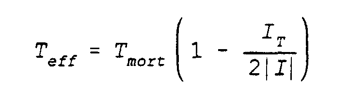
Pour I < IT, l'effet du temps mort est équivalent
à un délai Teff :
De cette manière, on compenser ainsi l'effet réel d'un temps mort lors de la commutation vers la fermeture et on réduit le niveau d'harmonique 6 côté alimentation.In this way, we thus compensate for the real effect a dead time when switching to closing and we reduce the harmonic level 6 on the power supply side.
Il convient de noter que l'on peut envisager dans certains cas, et plus particulièrement dans le cas où un courant est faible et quel que soit le sens de ce courant, de ne pas utiliser de consignes corrigées. En effet, dans le cas de faibles courants, l'influence de ces corrections est relativement limitée.It should be noted that one can consider in certain cases, and more particularly in the case where a current is weak and whatever the direction of this current, not to use corrected instructions. Indeed, in the in the case of weak currents, the influence of these corrections is relatively limited.
On a également représenté aux figures 7 l'allure générale des courants moteur soit dans le cas où l'on n'applique pas le procédé selon la présente invention (fig. 7a), soit dans le cas où on applique ce procédé (fig. 7b), pour un onduleur sans snubber.FIGS. 7 also shows the pace general of the motor currents either in the case where does not apply the method according to the present invention (fig. 7a), either in the case where this process is applied (fig. 7b), for an inverter without snubber.
En particulier, on observe l'élimination de la distorsion due à la présence d'un temps mort qui se présente dans le cas où l'on n'utilise pas de consignes corrigées en appliquant le procédé selon la présente invention.In particular, we observe the elimination of distortion due to the presence of a dead time which occurs if you do not use instructions corrected in applying the method according to the present invention.
On a représenté aux figures 8 les harmoniques 5 et 7 côté courant ainsi que l'harmonique 6 côté alimentation, d'une part dans le cas où l'on n'applique pas le procédé selon la présente invention (voir figs. 8a et 8b) et d'autre part dans le cas où l'on applique ce procédé (figs. 8c et 8d).FIGS. 8 show the harmonics 5 and 7 on the current side as well as the harmonic 6 on the power supply side, on the one hand in the case where the process is not applied according to the present invention (see figs. 8a and 8b) and other part in the case where this process is applied (figs. 8c and 8d).
On observe à nouveau que les harmoniques 5 et 7 dans le moteur dues à la présence d'un temps mort lors des commutations ont fortement diminué, tandis que l'harmonique 6 vue côté alimentation est ramenée à des valeurs négligeables.We again observe that harmonics 5 and 7 in the engine due to the presence of a dead time during commutations decreased sharply, while the harmonic 6 feed side view is reduced to values negligible.
Exactement les mêmes performances peuvent être obtenues pour un onduleur avec snubber.Exactly the same performance can be obtained for an inverter with snubber.
Claims (5)
- Method for processing PWM waves intended to control a voltage inverter or a voltage rectifier, this inverter or rectifier comprising at least a branch with at least one pair of switches (S1, DR1, S2, DR2) connected in series, through which a modulator creates the set PWM wave as a succession of high and low states, the high state being defined by the fact that the switch connected to the most positive load is closed whereas the switch connected to the most negative load is open, and the lower state being defined by the reverse, characterized by the fact that the set PWM wave is corrected according to the direction of the current leaving or entering the branch in order to obtain two corrected set signals, the corrected set signal for the output current presenting a high state supplemented by a delay on transition from the high state to the low state and the corrected set signal for the input current presenting a low state supplemented by a delay on transition from the low state to the high state.
- Method according to Claim 1, characterized in that the delay introduced into the corrected set signals corresponds essentially to the dead time itself introduced by the discriminator during the operation of closing the switches, this being in the case when an inverter or a rectifier is used without a switching-aid cell.
- Method according to Claim 1, characterized in that the delay introduced into the corrected set signals depends not only on the direction of the current but also on its value, this being in the case when an inverter or a rectifier is used with a switching-aid cell.
- Device for implementing the method for processing PWM waves according to any one of the preceding claims and which are intended to control a voltage inverter or a voltage rectifier, the inverter or the rectifier comprising at least a branch with at least one pair of switches (S1, DR1, S2, DR2) connected in series, the device comprising a modulator which creates the set PWM wave as a succession of high and low states, the high state being defined by the fact that the switch connected to the most positive load is closed whereas the switch connected to the most negative load is open, and the low state being defined by the reverse, characterized by the fact that correcting means correct the set PWM wave according to the direction of the current entering or leaving the branch of the inverter in order to obtain two corrected set signals, a corrected set signal for the output current presenting a high state supplemented by a delay on transition from the high state to the low state and a corrected set signal for the input current presenting a low state supplemented by a delay on transition from the low state to the high state.
- Use of the method according to any one of Claims 1 to 3 or of the device according to Claim 4 for an inverter or a voltage-controlled rectifier with or without a switching-aid cell, having two levels or having multiple levels.
Priority Applications (2)
| Application Number | Priority Date | Filing Date | Title |
|---|---|---|---|
| EP96908936A EP0821844B1 (en) | 1995-04-21 | 1996-04-12 | Method for processing pwm waves and devices therefor |
| GR20000401208T GR3033517T3 (en) | 1995-04-21 | 2000-05-26 | Method for processing pwm waves and devices therefor |
Applications Claiming Priority (6)
| Application Number | Priority Date | Filing Date | Title |
|---|---|---|---|
| EP95870040 | 1995-04-21 | ||
| EP95870040 | 1995-04-21 | ||
| EP95870058 | 1995-05-22 | ||
| EP95870058 | 1995-05-22 | ||
| PCT/BE1996/000039 WO1996033548A1 (en) | 1995-04-21 | 1996-04-12 | Method for processing pwm waves and devices therefor |
| EP96908936A EP0821844B1 (en) | 1995-04-21 | 1996-04-12 | Method for processing pwm waves and devices therefor |
Publications (2)
| Publication Number | Publication Date |
|---|---|
| EP0821844A1 EP0821844A1 (en) | 1998-02-04 |
| EP0821844B1 true EP0821844B1 (en) | 2000-03-15 |
Family
ID=26140796
Family Applications (1)
| Application Number | Title | Priority Date | Filing Date |
|---|---|---|---|
| EP96908936A Expired - Lifetime EP0821844B1 (en) | 1995-04-21 | 1996-04-12 | Method for processing pwm waves and devices therefor |
Country Status (21)
| Country | Link |
|---|---|
| US (1) | US5991176A (en) |
| EP (1) | EP0821844B1 (en) |
| JP (1) | JP3677048B2 (en) |
| KR (1) | KR100401120B1 (en) |
| CN (1) | CN1053530C (en) |
| AT (1) | ATE190777T1 (en) |
| AU (1) | AU703257B2 (en) |
| BR (1) | BR9608055A (en) |
| CA (1) | CA2218738C (en) |
| CZ (1) | CZ293168B6 (en) |
| DE (1) | DE69607157T2 (en) |
| DK (1) | DK0821844T3 (en) |
| EA (1) | EA000501B1 (en) |
| ES (1) | ES2144732T3 (en) |
| GR (1) | GR3033517T3 (en) |
| HU (1) | HU226738B1 (en) |
| PL (1) | PL182302B1 (en) |
| PT (1) | PT821844E (en) |
| SK (1) | SK141797A3 (en) |
| TR (1) | TR199701200T1 (en) |
| WO (1) | WO1996033548A1 (en) |
Families Citing this family (12)
| Publication number | Priority date | Publication date | Assignee | Title |
|---|---|---|---|---|
| JPH1132481A (en) * | 1997-07-08 | 1999-02-02 | Media Technol:Kk | Switching regulator |
| US6714424B2 (en) | 2001-11-30 | 2004-03-30 | Ballard Power Systems Corporation | Dead-time compensation with narrow pulse elimination in solid- state switch devices |
| US6690135B2 (en) * | 2002-01-24 | 2004-02-10 | Delphi Technologies, Inc. | Method for compensating for dead time non-linearities in a pulse width modulation controlled switching scheme |
| US7239535B2 (en) * | 2004-08-31 | 2007-07-03 | Abb Technology Ltd. | Voltage source converter |
| JP4581574B2 (en) * | 2004-09-08 | 2010-11-17 | 株式会社ジェイテクト | Motor control device and electric power steering device |
| TW201240298A (en) * | 2011-03-21 | 2012-10-01 | Motech Ind Inc | Inverter for converting a direct current voltage into an alternating current voltage and method thereof |
| US20130193766A1 (en) | 2012-01-31 | 2013-08-01 | Atlantic Grid Operations A., Llc | Control and protection of a dc power grid |
| DE102012206721A1 (en) * | 2012-04-24 | 2013-10-24 | Bayerische Motoren Werke Aktiengesellschaft | Method for controlling high-side switching element and low-side switching element, involves shortening time period of high state of control signals to duty cycle setting time period by twice guard time and fraction of guard time |
| CN104734474B (en) * | 2013-12-23 | 2017-07-18 | 立锜科技股份有限公司 | Switched power supply and its control circuit and control method |
| US9960608B2 (en) | 2016-03-04 | 2018-05-01 | Qualcomm Incorporated | High frequency multi-level rectification |
| DE102020200683A1 (en) | 2020-01-22 | 2021-07-22 | Zf Friedrichshafen Ag | Method for controlling an inverter of an electrical machine for a motor vehicle |
| DE102022201487A1 (en) | 2022-02-14 | 2023-08-17 | Zf Friedrichshafen Ag | Method for driving a circuit arrangement for power semiconductors |
Family Cites Families (11)
| Publication number | Priority date | Publication date | Assignee | Title |
|---|---|---|---|---|
| CN1013332B (en) * | 1988-03-06 | 1991-07-24 | 陕西机械学院 | Controller of pulsewidth modulation inverter by using micro processor |
| US5072354A (en) * | 1989-05-16 | 1991-12-10 | Mitsubishi Denki Kabushiki Kaisha | Pulse-width modulation type inverter apparatus |
| GB2238188B (en) * | 1989-05-16 | 1993-12-22 | Mitsubishi Electric Corp | Pulse-width modulation type inverter apparatus |
| JPH078146B2 (en) * | 1989-05-23 | 1995-01-30 | 春日電機株式会社 | Inverter control device |
| DE4016286A1 (en) * | 1990-05-21 | 1991-11-28 | Bosch Gmbh Robert | METHOD FOR PULSE WIDTH MODULATION FOR A CONVERTER |
| US5436819A (en) * | 1991-07-25 | 1995-07-25 | Mitsubishi Denki Kabushiki Kaisha | Apparatus for and method of compensating for an output voltage error in an inverter output |
| FR2693325B1 (en) * | 1992-07-03 | 1994-08-26 | Montpellier Ii Universite | Method for controlling switches, in particular bidirectional switches, control devices for implementing this process and converter thus controlled. |
| US5450306A (en) * | 1992-12-07 | 1995-09-12 | Square D Company | Closed loop pulse width modulator inverter with volt-seconds feedback control |
| JP2768206B2 (en) * | 1993-03-30 | 1998-06-25 | 三菱電機株式会社 | Inverter device |
| JPH08289561A (en) * | 1995-02-14 | 1996-11-01 | Toshiba Corp | Power converter |
| US5646837A (en) * | 1995-12-19 | 1997-07-08 | Performance Controls, Inc. | Pulse-width modulated circuit with improved linearity |
-
1996
- 1996-04-12 CA CA002218738A patent/CA2218738C/en not_active Expired - Lifetime
- 1996-04-12 KR KR1019970707353A patent/KR100401120B1/en not_active IP Right Cessation
- 1996-04-12 ES ES96908936T patent/ES2144732T3/en not_active Expired - Lifetime
- 1996-04-12 DE DE69607157T patent/DE69607157T2/en not_active Expired - Lifetime
- 1996-04-12 PT PT96908936T patent/PT821844E/en unknown
- 1996-04-12 SK SK1417-97A patent/SK141797A3/en unknown
- 1996-04-12 BR BR9608055-8A patent/BR9608055A/en not_active IP Right Cessation
- 1996-04-12 TR TR97/01200T patent/TR199701200T1/en unknown
- 1996-04-12 US US08/954,864 patent/US5991176A/en not_active Expired - Lifetime
- 1996-04-12 EA EA199700238A patent/EA000501B1/en not_active IP Right Cessation
- 1996-04-12 JP JP53136096A patent/JP3677048B2/en not_active Expired - Fee Related
- 1996-04-12 PL PL96323106A patent/PL182302B1/en unknown
- 1996-04-12 CN CN96193385A patent/CN1053530C/en not_active Expired - Lifetime
- 1996-04-12 CZ CZ19973219A patent/CZ293168B6/en not_active IP Right Cessation
- 1996-04-12 EP EP96908936A patent/EP0821844B1/en not_active Expired - Lifetime
- 1996-04-12 AU AU52625/96A patent/AU703257B2/en not_active Expired
- 1996-04-12 AT AT96908936T patent/ATE190777T1/en active
- 1996-04-12 HU HU9900066A patent/HU226738B1/en unknown
- 1996-04-12 WO PCT/BE1996/000039 patent/WO1996033548A1/en active IP Right Grant
- 1996-04-12 DK DK96908936T patent/DK0821844T3/en active
-
2000
- 2000-05-26 GR GR20000401208T patent/GR3033517T3/en unknown
Also Published As
| Publication number | Publication date |
|---|---|
| BR9608055A (en) | 1999-11-30 |
| HUP9900066A2 (en) | 1999-04-28 |
| EA000501B1 (en) | 1999-08-26 |
| KR100401120B1 (en) | 2004-12-31 |
| CZ293168B6 (en) | 2004-02-18 |
| EA199700238A1 (en) | 1998-02-26 |
| PL182302B1 (en) | 2001-12-31 |
| HUP9900066A3 (en) | 1999-11-29 |
| DK0821844T3 (en) | 2000-08-21 |
| ATE190777T1 (en) | 2000-04-15 |
| PT821844E (en) | 2000-09-29 |
| TR199701200T1 (en) | 1998-03-21 |
| ES2144732T3 (en) | 2000-06-16 |
| PL323106A1 (en) | 1998-03-16 |
| MX9708086A (en) | 1998-07-31 |
| HU226738B1 (en) | 2009-08-28 |
| CZ321997A3 (en) | 1998-01-14 |
| WO1996033548A1 (en) | 1996-10-24 |
| CN1182507A (en) | 1998-05-20 |
| CA2218738C (en) | 2008-10-07 |
| US5991176A (en) | 1999-11-23 |
| JP3677048B2 (en) | 2005-07-27 |
| DE69607157D1 (en) | 2000-04-20 |
| AU703257B2 (en) | 1999-03-25 |
| KR19990007830A (en) | 1999-01-25 |
| JPH11503900A (en) | 1999-03-30 |
| DE69607157T2 (en) | 2000-11-16 |
| CA2218738A1 (en) | 1996-10-24 |
| EP0821844A1 (en) | 1998-02-04 |
| AU5262596A (en) | 1996-11-07 |
| SK141797A3 (en) | 1998-06-03 |
| GR3033517T3 (en) | 2000-09-29 |
| CN1053530C (en) | 2000-06-14 |
Similar Documents
| Publication | Publication Date | Title |
|---|---|---|
| EP0821844B1 (en) | Method for processing pwm waves and devices therefor | |
| EP2355331B1 (en) | Converter apparatus and supply equipped with such apparatus | |
| EP3232556B1 (en) | Method and system for controlling an electric motor control installation | |
| EP1964257B1 (en) | Polyphase voltage converter control method | |
| FR2744295A1 (en) | CIRCUIT FOR PROTECTING HIGH POWER SWITCHING DEVICES | |
| EP0720281B1 (en) | Electronic device for electric energy conversion | |
| EP0933858A1 (en) | Method of protection by means of short-circuiting | |
| EP1964256B1 (en) | Method for controlling a polyphase voltage inverter | |
| FR2557753A1 (en) | ELECTRICAL CONTROL DEVICE AND EXCITATION CIRCUIT FOR ELECTRICAL CHARGE | |
| WO1981003722A1 (en) | Transistor or thyristor inverter with energy recovery | |
| FR2606228A1 (en) | DEVICE FOR CONTROLLING THE OUTPUT OF A HIGH FREQUENCY POWER SUPPLY UNIT | |
| FR2952483A1 (en) | CONVERTER DEVICE AND POWER SUPPLY WITHOUT INTERRUPTION EQUIPPED WITH SUCH A DEVICE. | |
| EP1835610A1 (en) | Parameterization method for a converter and converter implementing the method | |
| EP0336019B2 (en) | Multilevel pulse width modulation modulator | |
| FR2940863A1 (en) | POWER SUPPLY OF AN AIRCRAFT | |
| EP0670624B1 (en) | Switching power supply adapted for allowing reduced voltage commutations | |
| EP0344067B1 (en) | Linearisation process for a dc-dc converter, and method for carrying it out | |
| EP0616415A1 (en) | Control device for the oscillating circuit of a voltage inverter with quasi-resonant operation and PWM regulation | |
| EP2595296B1 (en) | Control system comprising an inverter module used as an active rectifier | |
| EP2182622B1 (en) | Circuit for power factor correction | |
| CA1211499A (en) | Control circuit for a synchronous motor with two windings | |
| EP2647112B1 (en) | Variable speed drive provided with a common-mode filtering device | |
| EP2293422B1 (en) | Converter of one direct current to another direct current with control signal interleaving, and power supply system including such a converter | |
| CA1108693A (en) | Self-contained pulse width modulation inverter | |
| EP2656492A2 (en) | Ac/dc power converter with improved power factor and improved thdi |
Legal Events
| Date | Code | Title | Description |
|---|---|---|---|
| PUAI | Public reference made under article 153(3) epc to a published international application that has entered the european phase |
Free format text: ORIGINAL CODE: 0009012 |
|
| 17P | Request for examination filed |
Effective date: 19970901 |
|
| AK | Designated contracting states |
Kind code of ref document: A1 Designated state(s): AT BE CH DE DK ES FI FR GB GR IE IT LI LU MC NL PT SE |
|
| 17Q | First examination report despatched |
Effective date: 19980326 |
|
| GRAG | Despatch of communication of intention to grant |
Free format text: ORIGINAL CODE: EPIDOS AGRA |
|
| GRAH | Despatch of communication of intention to grant a patent |
Free format text: ORIGINAL CODE: EPIDOS IGRA |
|
| GRAH | Despatch of communication of intention to grant a patent |
Free format text: ORIGINAL CODE: EPIDOS IGRA |
|
| RAP1 | Party data changed (applicant data changed or rights of an application transferred) |
Owner name: ALSTHOM BELGIUM S.A. |
|
| RAP3 | Party data changed (applicant data changed or rights of an application transferred) |
Owner name: ALSTOM BELGIUM S.A. |
|
| GRAA | (expected) grant |
Free format text: ORIGINAL CODE: 0009210 |
|
| AK | Designated contracting states |
Kind code of ref document: B1 Designated state(s): AT BE CH DE DK ES FI FR GB GR IE IT LI LU MC NL PT SE |
|
| REF | Corresponds to: |
Ref document number: 190777 Country of ref document: AT Date of ref document: 20000415 Kind code of ref document: T |
|
| REG | Reference to a national code |
Ref country code: CH Ref legal event code: EP |
|
| REF | Corresponds to: |
Ref document number: 69607157 Country of ref document: DE Date of ref document: 20000420 |
|
| REG | Reference to a national code |
Ref country code: CH Ref legal event code: NV Representative=s name: ABREMA AGENCE BREVETS ET MARQUES GANGUILLET & HUMP |
|
| GBT | Gb: translation of ep patent filed (gb section 77(6)(a)/1977) |
Effective date: 20000410 |
|
| REG | Reference to a national code |
Ref country code: IE Ref legal event code: FG4D Free format text: FRENCH |
|
| ITF | It: translation for a ep patent filed |
Owner name: MARCHI & PARTNERS S.R.L. |
|
| REG | Reference to a national code |
Ref country code: ES Ref legal event code: FG2A Ref document number: 2144732 Country of ref document: ES Kind code of ref document: T3 |
|
| REG | Reference to a national code |
Ref country code: DK Ref legal event code: T3 |
|
| REG | Reference to a national code |
Ref country code: PT Ref legal event code: SC4A Free format text: AVAILABILITY OF NATIONAL TRANSLATION Effective date: 20000615 |
|
| PLBE | No opposition filed within time limit |
Free format text: ORIGINAL CODE: 0009261 |
|
| STAA | Information on the status of an ep patent application or granted ep patent |
Free format text: STATUS: NO OPPOSITION FILED WITHIN TIME LIMIT |
|
| 26N | No opposition filed | ||
| REG | Reference to a national code |
Ref country code: GB Ref legal event code: IF02 |
|
| PGFP | Annual fee paid to national office [announced via postgrant information from national office to epo] |
Ref country code: IE Payment date: 20030408 Year of fee payment: 8 |
|
| PGFP | Annual fee paid to national office [announced via postgrant information from national office to epo] |
Ref country code: MC Payment date: 20030430 Year of fee payment: 8 |
|
| PG25 | Lapsed in a contracting state [announced via postgrant information from national office to epo] |
Ref country code: IE Free format text: LAPSE BECAUSE OF NON-PAYMENT OF DUE FEES Effective date: 20040412 |
|
| PG25 | Lapsed in a contracting state [announced via postgrant information from national office to epo] |
Ref country code: MC Free format text: LAPSE BECAUSE OF NON-PAYMENT OF DUE FEES Effective date: 20040430 |
|
| REG | Reference to a national code |
Ref country code: IE Ref legal event code: MM4A |
|
| PGFP | Annual fee paid to national office [announced via postgrant information from national office to epo] |
Ref country code: LU Payment date: 20100427 Year of fee payment: 15 |
|
| PGFP | Annual fee paid to national office [announced via postgrant information from national office to epo] |
Ref country code: PT Payment date: 20100405 Year of fee payment: 15 Ref country code: FI Payment date: 20100416 Year of fee payment: 15 Ref country code: DK Payment date: 20100413 Year of fee payment: 15 |
|
| PGFP | Annual fee paid to national office [announced via postgrant information from national office to epo] |
Ref country code: SE Payment date: 20100415 Year of fee payment: 15 |
|
| PGFP | Annual fee paid to national office [announced via postgrant information from national office to epo] |
Ref country code: GR Payment date: 20100429 Year of fee payment: 15 |
|
| REG | Reference to a national code |
Ref country code: PT Ref legal event code: MM4A Free format text: LAPSE DUE TO NON-PAYMENT OF FEES Effective date: 20111012 |
|
| REG | Reference to a national code |
Ref country code: SE Ref legal event code: EUG |
|
| REG | Reference to a national code |
Ref country code: GR Ref legal event code: ML Ref document number: 20000401208 Country of ref document: GR Effective date: 20111102 |
|
| PG25 | Lapsed in a contracting state [announced via postgrant information from national office to epo] |
Ref country code: PT Free format text: LAPSE BECAUSE OF NON-PAYMENT OF DUE FEES Effective date: 20111012 Ref country code: FI Free format text: LAPSE BECAUSE OF NON-PAYMENT OF DUE FEES Effective date: 20110412 |
|
| REG | Reference to a national code |
Ref country code: DK Ref legal event code: EBP |
|
| PG25 | Lapsed in a contracting state [announced via postgrant information from national office to epo] |
Ref country code: GR Free format text: LAPSE BECAUSE OF NON-PAYMENT OF DUE FEES Effective date: 20111102 |
|
| PG25 | Lapsed in a contracting state [announced via postgrant information from national office to epo] |
Ref country code: DK Free format text: LAPSE BECAUSE OF NON-PAYMENT OF DUE FEES Effective date: 20110430 |
|
| PG25 | Lapsed in a contracting state [announced via postgrant information from national office to epo] |
Ref country code: SE Free format text: LAPSE BECAUSE OF NON-PAYMENT OF DUE FEES Effective date: 20110413 |
|
| PG25 | Lapsed in a contracting state [announced via postgrant information from national office to epo] |
Ref country code: LU Free format text: LAPSE BECAUSE OF NON-PAYMENT OF DUE FEES Effective date: 20110412 |
|
| REG | Reference to a national code |
Ref country code: FR Ref legal event code: PLFP Year of fee payment: 20 |
|
| PGFP | Annual fee paid to national office [announced via postgrant information from national office to epo] |
Ref country code: NL Payment date: 20150420 Year of fee payment: 20 |
|
| PGFP | Annual fee paid to national office [announced via postgrant information from national office to epo] |
Ref country code: GB Payment date: 20150420 Year of fee payment: 20 Ref country code: DE Payment date: 20150421 Year of fee payment: 20 Ref country code: ES Payment date: 20150417 Year of fee payment: 20 Ref country code: CH Payment date: 20150420 Year of fee payment: 20 |
|
| PGFP | Annual fee paid to national office [announced via postgrant information from national office to epo] |
Ref country code: BE Payment date: 20150420 Year of fee payment: 20 Ref country code: FR Payment date: 20150421 Year of fee payment: 20 Ref country code: AT Payment date: 20150421 Year of fee payment: 20 Ref country code: IT Payment date: 20150427 Year of fee payment: 20 |
|
| REG | Reference to a national code |
Ref country code: DE Ref legal event code: R071 Ref document number: 69607157 Country of ref document: DE |
|
| REG | Reference to a national code |
Ref country code: NL Ref legal event code: MK Effective date: 20160411 |
|
| REG | Reference to a national code |
Ref country code: CH Ref legal event code: PL |
|
| REG | Reference to a national code |
Ref country code: GB Ref legal event code: PE20 Expiry date: 20160411 |
|
| REG | Reference to a national code |
Ref country code: AT Ref legal event code: MK07 Ref document number: 190777 Country of ref document: AT Kind code of ref document: T Effective date: 20160412 |
|
| REG | Reference to a national code |
Ref country code: ES Ref legal event code: FD2A Effective date: 20160727 |
|
| PG25 | Lapsed in a contracting state [announced via postgrant information from national office to epo] |
Ref country code: GB Free format text: LAPSE BECAUSE OF EXPIRATION OF PROTECTION Effective date: 20160411 |
|
| PG25 | Lapsed in a contracting state [announced via postgrant information from national office to epo] |
Ref country code: ES Free format text: LAPSE BECAUSE OF EXPIRATION OF PROTECTION Effective date: 20160413 |