EP0820157A2 - Verfahren zur digitalen Differenzialdemodulation - Google Patents
Verfahren zur digitalen Differenzialdemodulation Download PDFInfo
- Publication number
- EP0820157A2 EP0820157A2 EP97401680A EP97401680A EP0820157A2 EP 0820157 A2 EP0820157 A2 EP 0820157A2 EP 97401680 A EP97401680 A EP 97401680A EP 97401680 A EP97401680 A EP 97401680A EP 0820157 A2 EP0820157 A2 EP 0820157A2
- Authority
- EP
- European Patent Office
- Prior art keywords
- sample
- rank
- samples
- symbol
- signal
- Prior art date
- Legal status (The legal status is an assumption and is not a legal conclusion. Google has not performed a legal analysis and makes no representation as to the accuracy of the status listed.)
- Granted
Links
Images


Classifications
-
- H—ELECTRICITY
- H04—ELECTRIC COMMUNICATION TECHNIQUE
- H04B—TRANSMISSION
- H04B1/00—Details of transmission systems, not covered by a single one of groups H04B3/00 - H04B13/00; Details of transmission systems not characterised by the medium used for transmission
- H04B1/69—Spread spectrum techniques
- H04B1/707—Spread spectrum techniques using direct sequence modulation
- H04B1/7073—Synchronisation aspects
- H04B1/7075—Synchronisation aspects with code phase acquisition
- H04B1/70755—Setting of lock conditions, e.g. threshold
Definitions
- the present invention relates to a digital differential demodulation method. It finds application in so-called code division multiple access transmission systems, or CDMA for short. Such a technique is used in radio mobile systems.
- Code-division multiple access as a technique for sharing the radio channel, is often considered as the basis for defining future third-generation radio mobile systems. It is also used in some current telecommunications systems with land mobiles or satellites [1]. It allows simultaneous occupation of the same radio channel by signals transmitted by several or to several mobile terminals. This type of cohabitation specific to CDMA is only made possible by the use of spread spectrum modulation.
- the transmitted signal occupies a much wider frequency band than the band necessary for transmission.
- conventional modulation [6].
- the spreading factor which is the ratio of the occupied band to the transmitted information rate, is an important parameter. In the system cited in reference [1], it is 128.
- the spread spectrum modulation technique is a particularly flexible access technique. It is indeed possible to transmit signals simultaneously in the same frequency band without any coordination.
- the AMRC arouses a very particular interest insofar as it offers the opportunity of an original treatment of the multiple paths generated by the propagation.
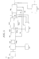
- FIG. 1 The principle diagram for CDMA modulation and demodulation is illustrated in FIG. 1 attached.
- This schematic diagram is voluntarily simplified, in particular there does not appear there the stages RF (radiofrequency) which make it possible, on transmission, to transpose and transmit the signal in the allocated frequency band, and at reception, to recover the signal in the allocated frequency band and transpose it to the base band where it will be processed.
- This figure shows, on the one hand, a spectrum spreading circuit 20 used for transmission and, on the other hand, a suitable filtering circuit 30, used for reception.
- the spread spectrum circuit 20 used for transmission receives information consisting of a series of binary symbols denoted a (k), where k is an index marking the rank of the symbol. These symbols can be received directly from an information source, where, as illustrated in FIG. 1, from a corrector coding circuit 10, which receives the raw information on its input 12 and delivers the protected information on its output 14.
- the frequency information symbols is noted Hs.
- the spread spectrum circuit 20 first comprises a spread sequence generator 22.
- This sequence is formed by a series of binary elements called "chips".
- This sequence is generally pseudo-random.
- the chips are noted ⁇ (n), where n denotes the rank of the chip in the sequence. This rank runs from 0 to N-1 for the same sequence.
- Each information symbol a (k) is multiplied by all the chips of the sequence ⁇ (n) in a multiplier 24. At the output of this multiplier, there is therefore a signal consisting of N pulses of width Tc. With the previous notations, the following of these signals can be noted: ............................ a (k-1). ⁇ (N-1), a (k) . ⁇ (0), a (k) . ⁇ (1), a (k) . ⁇ (2), ..., a (k) . ⁇ (N- 1), a (k + 1) . ⁇ (0), ...
- Such a signal has a bit rate, expressed in chips per second, N times greater than the bit rate in information symbols.
- the spectrum has therefore been spread out in an N ratio.
- the spreading circuit 20 is completed by a filter 26 which is of the low-pass filter type.
- the complete transmitter also comprises other means which have not been shown because they are well known to those skilled in the art, such as for example a local oscillator for generating a carrier, a modulation circuit for this carrier, transmitting antenna, etc.
- the circuit 30 comprises, first of all, a low-pass filter 32, analogous to the filter 26 used on transmission, and a filter 36 adapted to the spreading sequence used on transmission. More precisely, the impulse response of the receiver filter is the time reversal of the pseudo-random sequence used in the transmitter.
- the matched filter 36 performs a convolution operation on the signal delivered by the first filter 32. The flow of pulses at the input of the matched filter 36 carrying out the convolution is equal to the bit rate Hc of the chips, but, after convolution, this flow falls to Hc / N or Hs.
- a circuit 40 decides the value of the information received as a function of the value of the convolution signal. The information is then restored on the general output 42.
- the information transmitted can be ordinary binary information, but it is most often information resulting from a prior operation known as differential coding.
- the symbols a (k) are obtained by a preliminary differential encoder, composed, for example, of a logic gate of the exclusive OR type and of a delay circuit, the gate combining a current bit with the bit which precedes. The symbols thus coded are then multiplied by the pseudo-random sequence which has been discussed.
- the modulation of the carrier it can be of any known type, but it is often preferred to use phase modulation, in particular phase modulation with two states, called MDP2.
- MDP2 phase modulation with two states
- the receiver it suffices to compare the phase of the current symbol with the phase of the previous symbol. The receiver therefore does not have to estimate the phase of the symbols, but only the phase difference between two successive symbols. Hence the "differential" nature of the process.
- Figure 2 illustrates the operation of the system by schematically representing some signals appearing in the chain.
- Binary information is shown on line (a). It is a series of binary symbols of period Ts, in this case the series +1, -1, -1, +1, -1.
- Line (b) illustrates the spreading sequence S formed of N chips, in this case 110100 (naturally, in practice, the number N is much greater than 6).
- Line (c) shows the result of the multiplication of the information signal of line (a) by the sequence S of line (b).
- the correlation signal delivered by the filter to the spreading sequence is represented on line (d). Correlation peaks appear in a background of noise, the sign of which allows the patterns + S and -S to be found. A decision can then be taken to restore the original information (line e).
- Optimal reception then consists in recognizing, in the signal received, the patterns: a1S (t-t1) + a2S (t-t2) + a3S (t-t3) + a4S (t-t4)
- the optimal receiver of FIG. 1 is then completed by a filtering adapted to the impulse response h (t) of the channel.
- the filtering adapted to the impulse response of the channel realizes a recombination of all the existing paths. This operation is partially performed in conventional rake receivers, [1], [3], which combine a limited number of paths.
- the filtering adapted to the received pulse being done at the bit rate of the chips, so that the receiver achieves the best possible performance with a given transmission channel, this bit rate must be high enough.
- this bit rate must be high enough.
- the existing routes can only be taken into account with a chip speed greater than 5 Mchips / s.
- Spread spectrum modulation is precisely a technique which makes it possible to discriminate the different paths constituting the transmission channel.
- the recombination of these paths provides very significant performance gains compared to a transmission which would have undergone an ordinary channel (known as Rayleigh) as will be seen below with reference to FIG. 7.
- the object of the invention is precisely to remedy these drawbacks.
- the invention proposes a demodulation method, one of the essential characteristics of which is to implement an asynchronous sampling of frequency twice the chip frequency, that is to say at the frequency 2Hc.
- a conventional optimal reception requires that we combine samples taken exactly at times t1, t2, t3, ...
- an asynchronous sampling at the rate of the chips, that is to say at the frequency Hc can lead to missing one, two, or even all the received paths, if the sampling instants do not exactly coincide with the instants t1, t2, t3. ..
- an asynchronous sampling at double rhythm that is to say twice the frequency of the chips (2Hc)
- 2Hc twice the frequency of the chips
- This quantity U (k, i) is used to make the decision on the binary value of the information received. This decision is made by comparing the quantity obtained to a threshold of zero value, as is customary in MDP2. This quantity can also be kept in analog form for a possible protection treatment against transmission errors.
- the method of the invention can also be implemented by limiting the calculation of the decision sample to only significant samples.
- a threshold can be used on the amplitude of the samples received. This threshold can be adjusted from the automatic gain control signal, which keeps the power of the demodulated signal at a constant level. This device is found in all transmitters / receivers for radio transmission, and it is also necessary for the proper functioning of a CDMA receiver. Full demodulation is then applied only to samples whose amplitude exceeds the threshold. This this procedure eliminates a number of noise samples.
- FIG. 4 shows the impulse response of the radio mobile channel as it appears at the output of the filter adapted to the spreading sequence (that is to say at the output of the filter 36 in the diagram of FIG. 1).
- These responses have a width at the base of the peaks equal to 2Tc but these peaks are narrow and, by taking a single sample every Tc seconds, it is very possible not to sample the signal correctly.
- the samples are therefore taken at the rate of two per chip. This cadence corresponds to an oversampling of the signal and makes it possible not to miss a journey.
- the advantage of this oversampling is that it does not require perfect location of each path as is the case in conventional rake receivers.
- the circuit 56 delivers two analog signals, traditionally identified by letters I and Q, which are the signals representing the parts of the signal received respectively in phase and in quadrature of phase with the signal produced by the local oscillator 54. These two signals, in phase and in quadrature, are delivered on two connections 58I , 58Q. This whole part of the receiver is classic. The signals are then sampled at the frequency 2Hc and filtered in the circuit 60. This digital filtering is adapted to the chip pulse form used for transmission in the filter 26 of FIG. 1.
- the circuit 60 therefore delivers , on two outputs 62I and 62Q, sequences of 2N samples per period Ts. These samples are then the subject of a filtering adapted to the spreading sequence used on transmission in two filters 64I and 64Q, which deliver two sampled signals which will be noted later, more simply, I and Q. These two signals are applied to a demodulator circuit 66, the output of which is connected to a decision circuit 67. Furthermore, the signals I and Q are sent to a synchronization circuit 68, which delivers both the clock Hc relating to the chips , which allows sampling in the circuit 60 and processing in the demodulator 66, and the clock Hs relating to the information symbols.
- FIG. 6 shows the architecture of the demodulator 66, which makes it possible to calculate the quantities previously defined.
- This demodulator firstly comprises a circuit 70 for calculating products of the form Z (k, i) .Z * (k-1, i) where Z (k, i) is a complex sample of ranks k and i and Z * (k-1, i) the complex conjugate sample of previous rank in the order k of the sequences but of the same rank i within a sequence.
- circuit 70 directly receives samples I and Q of rows k and i, which corresponds to Z (k, i), and samples I (k-1, i) and Q (k-1 , i) delayed by the duration Ts, that is to say delayed by 2N samples. These delayed samples are delivered by two delay circuits 72I, 72Q.
- the circuit 70 having formed the product Z (k, 1) .Z * (k-1, i), it takes the real part, ie U (k, i).
- a circuit 74 receives this signal and forms a weighted sum using weighting coefficients P (k, i) and this in a window going from rank M to rank P, ie:
- the circuit shown also comprises a circuit 76 which receives I and Q and calculates the square of Z (k, i). It also includes taken by a circuit 78 which calculates a quantity A (k, i) which is an average defined by:
- FIG. 7 illustrates the performance of the method of the invention. This figure represents the probability of error as a function of the level of the signal expressed in decibels, for several bit rates.
- the curves shown correspond to the GSM-TU channel with six paths except curve 60 which represents a RAYLEIGH channel.
- Curves 61, 62, 63 are the curves obtained with chip rates of 1, 2 and 4 Mchips / s respectively.
- Curve 64 is the ideal curve corresponding to a rake receiver with six branches, comprising six demodulators with parallel correlation, perfectly synchronized. This reference curve supposes ideal spreading sequences (auto-orthogonal) and cannot therefore be reached in a Qualcomm type system. It does not depend on the bit rate but implicitly assumes that this rate is high enough for the different paths to be separated (of the order of 4 to 5 Mchips / s).
- FIG. 7 clearly shows the influence of the bit rate on the performance of the digital integral differential demodulator.
- the chip pulses must have a duration of the order of the smallest delay separating two successive paths so that the demodulator can recombine the paths.
- Figure 7 shows above all that the digital integral differential demodulator provides performances very close to the ideal.
- the residual offset can be explained by the autocorrelation noise, insofar as the sequences used are not auto-orthogonal but simply pseudo-random, as in the Qualcomm system.
Landscapes
- Engineering & Computer Science (AREA)
- Computer Networks & Wireless Communication (AREA)
- Signal Processing (AREA)
- Digital Transmission Methods That Use Modulated Carrier Waves (AREA)
- Mobile Radio Communication Systems (AREA)
- Compression, Expansion, Code Conversion, And Decoders (AREA)
Applications Claiming Priority (2)
| Application Number | Priority Date | Filing Date | Title |
|---|---|---|---|
| FR9608866A FR2751499B1 (fr) | 1996-07-16 | 1996-07-16 | Procede de demodulation differentielle numerique |
| FR9608866 | 1996-07-16 |
Publications (3)
| Publication Number | Publication Date |
|---|---|
| EP0820157A2 true EP0820157A2 (de) | 1998-01-21 |
| EP0820157A3 EP0820157A3 (de) | 1998-01-28 |
| EP0820157B1 EP0820157B1 (de) | 2004-10-20 |
Family
ID=9494089
Family Applications (1)
| Application Number | Title | Priority Date | Filing Date |
|---|---|---|---|
| EP97401680A Expired - Lifetime EP0820157B1 (de) | 1996-07-16 | 1997-07-11 | Verfahren zur digitalen Differenzialdemodulation |
Country Status (4)
| Country | Link |
|---|---|
| US (1) | US5960045A (de) |
| EP (1) | EP0820157B1 (de) |
| DE (1) | DE69731260T2 (de) |
| FR (1) | FR2751499B1 (de) |
Cited By (2)
| Publication number | Priority date | Publication date | Assignee | Title |
|---|---|---|---|---|
| EP1475900A3 (de) * | 1999-09-10 | 2004-12-15 | Interdigital Technology Corporation | Störungsunterdrückung in einem Spreizspektrum-Kommunikationssystem |
| US6985515B2 (en) | 1999-09-10 | 2006-01-10 | Interdigital Technology Corporation | Interference cancellation in a spread spectrum communication system |
Families Citing this family (9)
| Publication number | Priority date | Publication date | Assignee | Title |
|---|---|---|---|---|
| US6539050B1 (en) | 1997-06-26 | 2003-03-25 | Hughes Electronics Corporation | Method for transmitting wideband signals via a communication system adapted for narrow-band signal transmission |
| US6396822B1 (en) | 1997-07-15 | 2002-05-28 | Hughes Electronics Corporation | Method and apparatus for encoding data for transmission in a communication system |
| US6510147B1 (en) | 1997-07-15 | 2003-01-21 | Hughes Electronics Corporation | Method and apparatus for orthogonally overlaying variable chip rate spread spectrum signals |
| US6185248B1 (en) * | 1998-03-12 | 2001-02-06 | Northrop Grumman Corporation | Wideband digital microwave receiver |
| FR2794586B1 (fr) | 1999-06-02 | 2001-08-03 | Commissariat Energie Atomique | Procede de traitement d'une reponse impulsionnelle avec seuil adaptatif et recepteur correspondant |
| US20040110508A1 (en) * | 2002-09-20 | 2004-06-10 | Jacobus Haartsen | Methods and electronic devices for wireless ad-hoc network communications using receiver determined channels and transmitted reference signals |
| KR100649678B1 (ko) | 2005-07-15 | 2006-11-27 | 삼성전기주식회사 | 가중치를 이용한 다중 차동 복조기 |
| KR100759514B1 (ko) | 2006-07-10 | 2007-09-18 | 삼성전기주식회사 | 무선 사설망 복조기 및 복조방법 |
| US9112754B2 (en) | 2013-10-08 | 2015-08-18 | Freescale Semiconductor, Inc. | Techniques for generating bit log-likelihood ratios in communication systems using differential modulation |
Citations (4)
| Publication number | Priority date | Publication date | Assignee | Title |
|---|---|---|---|---|
| US4969159A (en) * | 1989-03-22 | 1990-11-06 | Harris Corporation | Spread spectrum communication system employing composite spreading codes with matched filter demodulator |
| GB2233860A (en) * | 1989-07-13 | 1991-01-16 | Stc Plc | "Extending the range of radio transmissions" |
| WO1991015912A1 (en) * | 1990-04-09 | 1991-10-17 | Proxim, Inc. | Radio communication system using spread spectrum techniques |
| US5506862A (en) * | 1993-06-25 | 1996-04-09 | Digital Wireless Corp. | Digital implementation of spread spectrum communications system |
Family Cites Families (1)
| Publication number | Priority date | Publication date | Assignee | Title |
|---|---|---|---|---|
| US5754599A (en) * | 1996-01-04 | 1998-05-19 | Motorola, Inc. | Method and apparatus for coherent channel estimation in a communication system |
-
1996
- 1996-07-16 FR FR9608866A patent/FR2751499B1/fr not_active Expired - Fee Related
-
1997
- 1997-07-10 US US08/891,031 patent/US5960045A/en not_active Expired - Fee Related
- 1997-07-11 EP EP97401680A patent/EP0820157B1/de not_active Expired - Lifetime
- 1997-07-11 DE DE69731260T patent/DE69731260T2/de not_active Expired - Fee Related
Patent Citations (4)
| Publication number | Priority date | Publication date | Assignee | Title |
|---|---|---|---|---|
| US4969159A (en) * | 1989-03-22 | 1990-11-06 | Harris Corporation | Spread spectrum communication system employing composite spreading codes with matched filter demodulator |
| GB2233860A (en) * | 1989-07-13 | 1991-01-16 | Stc Plc | "Extending the range of radio transmissions" |
| WO1991015912A1 (en) * | 1990-04-09 | 1991-10-17 | Proxim, Inc. | Radio communication system using spread spectrum techniques |
| US5506862A (en) * | 1993-06-25 | 1996-04-09 | Digital Wireless Corp. | Digital implementation of spread spectrum communications system |
Cited By (10)
| Publication number | Priority date | Publication date | Assignee | Title |
|---|---|---|---|---|
| EP1475900A3 (de) * | 1999-09-10 | 2004-12-15 | Interdigital Technology Corporation | Störungsunterdrückung in einem Spreizspektrum-Kommunikationssystem |
| US6983008B2 (en) | 1999-09-10 | 2006-01-03 | Interdigital Technology Corporation | Base station for use in a CDMA communication system using an antenna array |
| US6985515B2 (en) | 1999-09-10 | 2006-01-10 | Interdigital Technology Corporation | Interference cancellation in a spread spectrum communication system |
| US7545846B2 (en) | 1999-09-10 | 2009-06-09 | Interdigital Technology Corporation | Interference cancellation in a spread spectrum communication system |
| US7684469B2 (en) | 1999-09-10 | 2010-03-23 | Interdigital Technology Corporation | Code division multiple access transmission antenna weighting |
| US7813413B2 (en) | 1999-09-10 | 2010-10-12 | Interdigital Technology Corporation | Antenna array communication using spreading codes |
| US7953139B2 (en) | 1999-09-10 | 2011-05-31 | Interdigital Technology Corporation | Interference cancellation in a spread spectrum communication system |
| US9036680B2 (en) | 1999-09-10 | 2015-05-19 | Interdigital Technology Corporation | Interference cancellation in a spread spectrum communication system |
| US9219522B2 (en) | 1999-09-10 | 2015-12-22 | Interdigital Technology Corporation | Code division multiple access transmission antenna weighting |
| US9270327B2 (en) | 1999-09-10 | 2016-02-23 | Interdigital Technology Corporation | Interference cancellation in a spread spectrum communication system |
Also Published As
| Publication number | Publication date |
|---|---|
| FR2751499B1 (fr) | 1998-08-28 |
| EP0820157A3 (de) | 1998-01-28 |
| DE69731260D1 (de) | 2004-11-25 |
| FR2751499A1 (fr) | 1998-01-23 |
| EP0820157B1 (de) | 2004-10-20 |
| US5960045A (en) | 1999-09-28 |
| DE69731260T2 (de) | 2005-11-17 |
Similar Documents
| Publication | Publication Date | Title |
|---|---|---|
| EP0113487B1 (de) | Verfahren zur Anwendung in einer Echounterdrückungseinrichtung zur Messung einer Echoverzögerung und Vorrichtung zur Durchführung des Verfahrens | |
| FR2642922A1 (fr) | Dispositif de communication sur spectre disperse | |
| FR2774831A1 (fr) | Recepteur adaptatif de signaux pour systeme de communications a acces pultiples par repartition a codes | |
| EP0630120A1 (de) | Synchronisationsverfahren in Funktelefonkommunikationen mit Kodemultiplex-Vielfachzugriff | |
| FR2737362A1 (fr) | Procede de selection des retards de propagation retenus pour recevoir des messages transmis par radiocommunication a etalement de spectre | |
| EP0013343A1 (de) | Verfahren und Vorrichtung zur Auffindung einer Pseudo-Zufallsfolge von 0 Grad- und 180 Grad-Phasenänderungen der Trägerwelle in einem Datenempfänger | |
| EP1260071B1 (de) | Verfahren und vorrichtung für kanalschäztung | |
| EP0820157B1 (de) | Verfahren zur digitalen Differenzialdemodulation | |
| EP0643504A1 (de) | Schwellendetektor für CDMA System | |
| FR2681488A1 (fr) | Dispositif de communication sur spectre disperse. | |
| EP2958245A1 (de) | Uwb-empfänger mit stabiler nachverfolgung der zeitverschiebung | |
| EP0629059B1 (de) | Digitales Spreizspektrumübertragungssystem mit Niederfrequenz-Pseudozufallkodierung von Nutzinformation und Verfahren zur Spektrumsspreizung und Spektrumskomprimierung zur Verwendung in einem solchen System | |
| WO2000011799A1 (fr) | Recepteur en rateau iteratif et procede de reception correspondant | |
| EP0849889B1 (de) | Verfahren zum Mehrwegesignalempfang | |
| FR3093257A1 (fr) | Méthode et dispositif de modulation par séquences de zadoff-chu | |
| EP1050987B1 (de) | CDMA-Vielfachzugriffverfahren mit verbesserter Kapazität | |
| EP0702467B1 (de) | Mittels Initialisierungsfolge synchronisierbares digitales Übertragungssystem | |
| EP1058402B1 (de) | Verfahren zur Verarbeitung eines Impulssignals mit einer adaptiven Schwelle und entsprechender Empfänger | |
| FR2691309A1 (fr) | Procédé de désétalement en réception d'un signal en large bande. | |
| FR2813474A1 (fr) | Procede de reception non coherente dp-mok avec combinaison de trajets multiples et recepteur correspondant | |
| FR2770058A1 (fr) | Procede de traitement d'un signal de transmission d'information par etalement de spectre et recepteur correspondant | |
| EP0497250B1 (de) | Verfahren zur Erkennung eines Störsignal für einen digitalen Datendemodulator, und Einrichtung zur Durchführung eines solchen Verfahrens | |
| WO2000028662A1 (fr) | Filtre numerique a architecture parallele et recepteur de signaux a etalement de spectre utilisant un tel filtre | |
| EP1252722B1 (de) | Cdma-funkübertragungsverfahren mit zugriffskodes und empfänger dafür | |
| EP1693969B9 (de) | CDMA-Empfangsverfahren mit paralleler Interferenzunterdrückung, entsprechende Stufe und Empfänger |
Legal Events
| Date | Code | Title | Description |
|---|---|---|---|
| PUAI | Public reference made under article 153(3) epc to a published international application that has entered the european phase |
Free format text: ORIGINAL CODE: 0009012 |
|
| PUAL | Search report despatched |
Free format text: ORIGINAL CODE: 0009013 |
|
| AK | Designated contracting states |
Kind code of ref document: A2 Designated state(s): AT BE CH DE DK ES FI FR GB GR IE IT LI LU MC NL PT SE |
|
| AK | Designated contracting states |
Kind code of ref document: A3 Designated state(s): AT BE CH DE DK ES FI FR GB GR IE IT LI LU MC NL PT SE |
|
| 17P | Request for examination filed |
Effective date: 19980706 |
|
| RBV | Designated contracting states (corrected) |
Designated state(s): DE GB |
|
| GRAH | Despatch of communication of intention to grant a patent |
Free format text: ORIGINAL CODE: EPIDOS IGRA |
|
| GRAH | Despatch of communication of intention to grant a patent |
Free format text: ORIGINAL CODE: EPIDOS IGRA |
|
| GRAA | (expected) grant |
Free format text: ORIGINAL CODE: 0009210 |
|
| AK | Designated contracting states |
Kind code of ref document: B1 Designated state(s): DE GB |
|
| REG | Reference to a national code |
Ref country code: GB Ref legal event code: FG4D Free format text: NOT ENGLISH |
|
| REF | Corresponds to: |
Ref document number: 69731260 Country of ref document: DE Date of ref document: 20041125 Kind code of ref document: P |
|
| GBT | Gb: translation of ep patent filed (gb section 77(6)(a)/1977) |
Effective date: 20050201 |
|
| PLBE | No opposition filed within time limit |
Free format text: ORIGINAL CODE: 0009261 |
|
| STAA | Information on the status of an ep patent application or granted ep patent |
Free format text: STATUS: NO OPPOSITION FILED WITHIN TIME LIMIT |
|
| 26N | No opposition filed |
Effective date: 20050721 |
|
| PGFP | Annual fee paid to national office [announced via postgrant information from national office to epo] |
Ref country code: DE Payment date: 20080730 Year of fee payment: 12 |
|
| PGFP | Annual fee paid to national office [announced via postgrant information from national office to epo] |
Ref country code: GB Payment date: 20080630 Year of fee payment: 12 |
|
| GBPC | Gb: european patent ceased through non-payment of renewal fee |
Effective date: 20090711 |
|
| PG25 | Lapsed in a contracting state [announced via postgrant information from national office to epo] |
Ref country code: GB Free format text: LAPSE BECAUSE OF NON-PAYMENT OF DUE FEES Effective date: 20090711 |
|
| PG25 | Lapsed in a contracting state [announced via postgrant information from national office to epo] |
Ref country code: DE Free format text: LAPSE BECAUSE OF NON-PAYMENT OF DUE FEES Effective date: 20100202 |