BACKGROUND OF THE INVENTION
This invention relates to a method of forming an
interlayer film, particularly to a method suited for forming
an interlayer insulating film in manufacturing semiconductor
devices.
In manufacturing semiconductor devices, a method is
often adopted in which fluid source materials are used to
form interlayer insulating films so as to fill up troughs on
a substrate surface formed by wiring patterns thereon to
assure a high smoothness of the substrate surface. When
using the fluid source material for forming the interlayer
insulating film, the fluid film, while it is being
deposited, flows into the troughs between patterns from the
top surfaces of the wiring patterns, resulting in filling
the troughs.
When forming such an interlayer insulating film, a
single step film deposition process is carried out in the
related method to obtain the desired film thickness (for
example, see M. Matsuura and M. Hirayama, 1995 Dry Process
Symposium, pp. 261-268 (1995)).
Such a method of forming interlayer insulating films,
however, causes an undesirable phenomenon that, when the
troughs on the substrate surface are formed by a plurality
of patterns of differing widths, the thickness of the film
formed on each of those patterns varies with dependence on
pattern widths (hereinafter, this phenomenon is referred to
as poor global smoothness), resulting in differences in
level. This is considered to be as follows. When the film
is deposited, the fluid film swells on each pattern due to
the surface tension. On a wide pattern, the film swells
more despite the fluid film flowing into the trough between
patterns from the edge of the pattern as the film becomes
thicker, so that when the film deposition ends, the film is
formed with a thickness as swelled and results in becoming
thicker than on a narrower pattern.
If an interlayer insulating film has such poor global
smoothness, there occurs problems such as the step coverage
of the formed interlayer insulating film becoming poor and a
wiring layer or the like becoming thin partially when formed
on the interlayer insulating film.
In view of foregoing, it is an object of this invention
to provide a method of forming an interlayer film, which can
eliminate the above phenomenon that the film formed on each
pattern becomes uneven in thickness due to differences in
width of those patterns formed on the substrate.
SUMMARY OF THE INVENTION
Above object is achieved by a method of forming an
interlayer film in which the interlayer film is formed by a
process comprising a plurality of steps in each of which a
portion of the film is deposited with the same source
material under a condition of providing the portion of film
with different fluidity.
In a method of forming an interlayer film according to
the first aspect of the present invention, a portion of the
interlayer film is at first deposited under a condition of
providing the portion of film with relatively reduced
fluidity, so that the film is deposited with an almost
uniform thickness regardless of any pattern width on the
substrate. After this, the rest portion of the film is
deposited under a condition of providing the rest portion of
the film with relatively increased fluidity so as to fill up
the trough between the patterns.
In a method of forming an interlayer film according to
the second aspect of the present invention, an undercoating
film is formed in advance which affects to reduce fluidity
of a portion of the interlayer film to be formed thereon, by
which the portion of the interlayer film is deposited with
an almost uniform thickness regardless of any pattern width
on the substrate. Then, using the same source material, the
rest portion of the film is deposited over the above portion
of the film under a condition of providing the rest portion
of the film with relatively increased fluidity.
BRIEF DESCRIPTION OF THE DRAWINGS
Fig. 1A through Fig. 1C are cross sectional side views
of a major part of a semiconductor device for illustrating
an embodiment of the present invention is successive
processing steps.
Fig. 2 is a schematic view showing a configuration of a
CVD apparatus appropriately used for embodying the present
invention.
Fig. 3A through Fig. 3D are cross sectional side views
of a major part of a semiconductor device for illustrating
the third embodiment of the present invention in successive
processing steps.
Fig. 4A through Fig. 4E are cross sectional side views
of a major part of a semiconductor device for illustrating
the fourth embodiment of the present invention in successive
processing steps.
DESCRIPTION OF THE PREFERRED EMBODIMENTS
In the following, a method of forming an interlayer
film according to the present invention will be explained in
detail with reference to some embodiments.
(First Embodiment)
This first embodiment is a method of forming an
interlayer film according to the first aspect of the present
invention and provides an interlayer film made of an SiO2
film by two steps of film forming processes, which will be
explained with reference to Figs. 1A through 1C.
Figure 1A shows a substrate for forming an interlayer
film. A substrate 1 is made of a silicon wafer. On this
substrate 1 are formed an Al wiring pattern 2 and an Al pad
pattern 3 via an oxide film or the like (not illustrated).
The Al wiring pattern 2 is formed to be 0.85 µm in height
and 0.4 µm in width. The Al pad pattern 3 is formed to be
0.85 µm in height and 100 µm in width. Between those Al
wiring pattern 2 and Al pad pattern 3 is provided an enough
space, with which each of those patterns becomes independent
of the other. In Figs. 1A through 1C, the wiring widths of
the Al wiring pattern 2 and the Al pad pattern 3 are
illustrated with different ratios for convenience.
In order to form an interlayer film on the substrate 1,
on which are formed the Al wiring pattern 2 and the Al pad
pattern 3 of differing widths, to fill up a trough due to
the patterns, an SiO2 film 4 is formed in a thickness of 0.4
µm using a well-known plasma CVD apparatus, and SiH4 and H2O2
as source materials at a film deposition temperature of 30
°C with the SiO2 film 4 covering the Al wiring pattern 2 and
the Al pad pattern 3 as shown in Fig. 1B.
The flow rate of the source material SiH4 was defined
to be 120 sccm. As for H2O2; hydrogen peroxide solution of
60% in concentration was introduced into the reduced
pressure CVD apparatus at a flow rate of 0.65 g/min and
instantaneously evaporated by a flasher immediately after
being introduced to react to SiH4. As a carrier gas, N2 was
used at a flow rate of 1000 sccm separately from the above
mentioned SiH4 and H2O2. The reaction pressure was set at
850 m Torr.
Above described SiH4 and H2O2 used as source materials
satisfy a condition for having fluidity when deposited.
Specifically, their fluidity is reduced at 20 °C or less
under the above mentioned flow rate of source material and
reaction pressure. Over 30 °C, their fluidity is almost
lost. On the other hand, their fluidity is increased
gradually under 20 °C. Especially, under 5 °C, their
fluidity increases significantly. Such a deposition
temperature dependent fluidity change is considered to be
due to a reaction mechanism of oxidizing SiH4 into Si(OH)4 by
an oxidant H2O2 and further dehydrating and condensing the
resultant Si(OH)4 into SiO2, in which mechanism the process
of dehydrating and condensing Si(OH)4 nearly in liquid
phase, into SiO2 in solid phase, is accelerated at high
temperatures and decelerated at low temperatures.
The SiO2 film 4 formed under such deposition conditions
is to be as a portion of the interlayer film in this
invention and, because of being formed at 30 °C, the film
has almost no fluidity when deposited. Consequently, the
film becomes almost even in thickness regardless of the
widths of the patterns 2 and 3 formed under the film. In
this stage, however, the film does not fill up the trough
between the patterns 2 and 3 yet.
After this, the SiO2 film 5, which is assumed as the
rest portion of the interlayer film in this invention, is
formed on the above mentioned SiO2 film 4 as shown in Fig.
1C in a thickness of 0.4 µm under the same conditions except
for the deposition temperature, which is changed to 0 °C.
Thus, an interlayer film 6 comprising the SiO2 film 4
together with the above SiO2 film 5 is obtained.
The SiO2 film 5 formed under such deposition conditions
has a high fluidity when deposited as mentioned above
because of the deposition temperature of 0 °C, so that the
film can fill up the trough formed on the SiO2 film 4 due to
the patterns 2 and 3. Consequently, the interlayer film 5
becomes to provide a satisfactory surface smoothness. In
other words, since patterns 2 and 3 are already covered by
the SiO2 film 4, the SiO2 film 5 formed on this film comes in
contact with the SiO2 film 4 without coming in direct
contact with the narrow Al wiring patter 2 and the wide Al
pad pattern 3 even on the patterns 2 and 3. Thus, the
underside of the SiO2 film 5 is completely occupied with the
SiO2 film 4 which provides a uniform wettability. Thus,
unlike the related art method, the SiO2 film 5 is not
affected by the surface tension on the patterns but is
affected only by gravitation when deposited. Consequently,
the film 5 can fill up the trough by the fluidity of the
film and the surface become smooth.
When an SiO2 film having a thickness of 0.8 µm is
formed using SiH4 and H2O2 as source materials in the state
shown in Fig. 1A by a single step deposition process without
being divided into two steps at a deposition temperature of
0 °C under the same conditions as mentioned above, the
difference in film thickness between the SiO2 films on the
Al wiring pattern 2 and the Al pad pattern 3 was 400 nm. In
this first embodiment, however, this difference in the film
thickness could be reduced down to 150 nm.
Furthermore, with the method in this first embodiment,
the difference in film thickness between the SiO2 film on a
plurality of the densely formed Al wiring patterns 2 and the
SiO2 film on a plurality of the densely formed Al pad
patterns 3 could be reduced by 110 nm compared with that
with the related art method in which a single step
deposition process is carried out.
As explained above, it is confirmed that this first
embodiment is very effective for preventing the global
smoothness from becoming poor.
In the above embodiment in which the second deposition
process is carried out just after the first one, plasma
exposure may be carried out onto the SiO2 film 4 just after
the first deposition process prior to the formation of the
SiO2 film 5. This plasma exposure hardens the plasma-exposed
surface of the SiO2 film 4, with which the film 4
loses its fluidity almost completely. Thus the SiO2 film 4
is prevented from flowing slightly to be affected by the
difference in widths of patterns 2 and 3 before the second
deposition process is carried out.
(Second Embodiment)
This second embodiment is also a method according to
the first aspect of the invention and is explained as a
method of forming an interlayer film with the plasma CVD
method and the reduced pressure CVD method as two steps of
deposition processes.
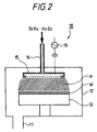
Figure 2 shows an apparatus that can carry out both
plasma CVD method and reduced pressure CVD method. This CVD
apparatus 10 is provided with a wafer stage 13 in vacuum
chamber 12 provided with an exhaust pipe 11 connected to a
vacuum pump (not illustrated). In the vacuum chamber 12 is
provided with a pipe 14 used for introducing source
materials specifically SiH4, H2O2, and a carrier gas (N2)
from a source material supply (not illustrated). To this
pipe 14 is connected a shower head 15 above the wafer stage
13 in the vacuum chamber 12, with the shower head 15 facing
the wafer stage 13. An RF oscillator 16 is connected to
this shower head 15 so that plasma is generated between this
shower head 15 and the wafer stage 13.
To carry out deposition of a film on a wafer W
(substrate 1 ) on which the Al wiring pattern 2 and the Al
pad pattern 3 are formed as shown in Fig. 1A by using such a
configuration of the CVD apparatus, at first the wafer W is
set on the wafer stage 13 as shown in Fig. 2, and in this
state, the vacuum pump is started to evacuate the vacuum
chamber 12 to the specified pressure. Then, the temperature
of the wafer W is adjusted to 0 °C and an RF power is
applied to between the shower head 15 and the wafer stage 13
by the RF oscillator 16 to generate plasma.
The source material is then introduced into plasma P
through the shower head 15 from the pipe 14 for reaction to
form an SiO2 film as shown in Fig. 1B. (Although the SiO2
film formed in this second embodiment differs from the SiO2
film formed in the first embodiment, a numeral 4 is also
assigned to the SiO2 film formed in this second embodiment
for convenience of the substrate explanation.)
The flow rates of SiH4 and H2O2 as source materials, as
well as N2 as a carrier gas were set to 120 sccm, 0.65
g/min, and 1000 sccm, respectively. The deposition pressure
was set at 850 m Torr.
Since the SiO2 film 4 thus formed under such deposition
conditions is assumed as a portion of the interlayer film in
this invention and the film is formed with the plasma CVD
method, the film does not flow when deposited.
Consequently, the film becomes almost even in thickness
regardless of the widths of the patterns 2 and 3 formed
under the film. In this stage, however, the film cannot
fill up the trough between the patterns 2 and 3 yet. Like
the case in the first embodiment.
Subsequently, introduction of the material is stopped,
and application of RF power by the RF oscillator 16 is
stopped to extinguish the plasma in the vacuum chamber 12.
After this, an SiO2 film 5 to be assumed as the rest
portion of the interlayer film in this invention as shown in
Fig. 1C is formed on the SiO2 film 4 without plasma
generation in a thickness of 0.4 µm under the same
conditions as those of the preceding deposition. Thus, the
interlayer film 6 comprising the SiO2 film 4 and 5 is
obtained. (Although the SiO2 film and the interlayer film
formed in this second embodiment differ from the SiO2 film 5
and the interlayer film 6 formed in the first embodiment,
numerals 5 and 6 are respectively assigned also to the SiO2
film and the interlayer film formed in this second
embodiment for convenience.)
Thus formed SiO2 film 5, being deposited under a
temperature of 0 °C, has high fluidity when deposited, so
that it can fill up the trough formed on the surface of the
SiO2 film 4 due to the Al wiring pattern 2 and the Al pad
pattern 3 like in the first embodiment. Consequently, the
interlayer film 5 is formed to have a satisfactory
smoothness.
When an SiO2 film having a thickness of 0.8 µm is
formed using SiH4 and H2O2 as source materials in the state
shown in Fig. 1A by a single step deposition process without
being divided into two steps at a deposition temperature of
0 °C under the same conditions as mentioned above, the
difference in film thickness between the SiO2 films on the
Al wiring pattern 2 and the Al pad pattern 3 was 400 nm as
mentioned above, but in this second embodiment, this
difference in film thickness could be reduced down to 170
nm.
Furthermore, with the method in this second embodiment,
the difference in film thickness between the SiO2 film on a
plurality of the densely formed Al wiring patterns 2 and the
SiO2 film formed on a plurality of the densely formed Al pad
patterns 3 could be reduced by 100 nm compared with that
with the related art method in which a single step
deposition process is carried out.
As explained above, it is confirmed that this second
embodiment is also very effective for preventing the global
smoothness from being poor.
Furthermore, in the first and second embodiments, SiH4
and H2O2 are used as source materials, but the materials are
not limited to them in this invention. For example, instead
of SiH4, Si2H6 and the like may be used, and, instead of H2O2,
an oxidizer dissolved in water such as ozone (O3) dissolved
in water or, furthermore, liquid nitrogen and the like may
be used.
In the first and second embodiments, two steps
deposition process are carried out to form the desired
interlayer film 6. The deposition process, however, may be
carried out by more than three steps for obtaining the
interlayer film 6 by carrying out the first deposition
process under a condition basically to reduce the fluidity
or prevent the fluidization, and then the subsequent
deposition processes under a condition to increase the
fluidity.
Furthermore, in the first embodiment, fluidity is
adjusted by changing a deposition temperature which is
adopted as a deposition condition to reduce or increase the
fluidity. However, the fluidity may also be adjusted by
changing the deposition pressure, the mixing rate of the
source materials, etc.
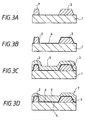
(Third Embodiment)
This third embodiment explains a method of forming an
interlayer film according to the second aspect of the
invention and provides the interlayer film made of an SiO2
film on an undercoating film by two steps of film forming
processes, which will be explained with reference to Figs.
3A through 3D.
Figure 3A shows a substrate for forming an interlayer
film. A substrate 1 is made of a silicon wafer. On this
substrate 1 are formed an Al wiring pattern 2 and an Al pad
patter 3 via an oxide film or the like (not illustrated).
The Al wiring pattern 2 is formed to be 0.85 µm in height
and 0.4 µm in width. The Al pad pattern 3 is formed to be
0.85 µm in height and 100 µm in width. Between those Al
wiring pattern 2 and Al pad pattern 3 is provided an enough
space, with which each of those patterns becomes independent
of the other. In Figs. 3A through 3D, the wiring widths of
the Al wiring pattern 2 and the Al pad pattern 3 are
illustrated with different ratios for convenience.
In order to form an interlayer film on the substrate 1,
on which are formed the Al wiring patter 2 and the Al pad
patter 3 of differing widths, to fill up a trough due to the
patterns, an undercoating film is at first formed before
forming the interlayer film. In this embodiment, a P-TEOS·SiO2
film 4 (undercoating film) is deposited in a
thickness of 0.1 µm with the P-TEOS·SiO2 film 4 covering the
Al wiring pattern 2 and the Al pad pattern 3 with a plasma
CVD method using a well-known plasma CVD apparatus, and
using TEOS (tetraethoxysilane) as a source material at a
film deposition temperature of 400 °C as shown in Fig. 3B.
Subsequently, the surface of this P-TEOS·SiO2 film 4 is
treated with hydroxylamine (NH2OH), which is a powerful
reducing agent. Then, the Si-O bonds of the P-TEOS·SiO2 film
4 are cut by the reduction treatment, so that the surface
becomes hydrophobic.
Subsequently, on the hydrophobic surface of the P-TEOS·SiO2
film 4 is formed an SiO2 film 5 (a portion of an
interlayer film in this invention) with the SiO2 film 5
covering both of the Al wiring pattern 2 and the Al pad
pattern 3 as shown in Fig. 3C. The SiO2 film 5 was
deposited at a film-deposition temperature of 0 °C using a
well-known reduced pressure CVD apparatus and using SiH4 and
H2O2 as source materials so as to obtain the SiO2 film with a
thickness of 0.4 µm.
The flow rate of the source material SiH4 was defined
to be 120 sccm. As for H2O2, hydrogen peroxide solution of
60% in concentration was introduced into the reduced
pressure CVD apparatus at a flow rate of 0.65 g/min and
instantaneously evaporated by a flasher immediately after
being introduced to react with SiH4. As a carrier gas, N2
was used at a flow rate of 1000 sccm separately from the
above mentioned SiH4 and H2O2. The reaction pressure was set
at 850 m Torr.
Above described SiH4 and H2O2 used as source materials
satisfy a condition for having fluidity when deposited.
Specifically, their fluidity increases at 20 °C or less
under the above mentioned flow rate of source material and
reaction pressure. Especially, under 5 °C, their fluidity
increases significantly. Above 20 °C, their fluidity
decreases and over 30 °C, their fluidity is almost lost.
Consequently, in this embodiment, the obtained SiO2
film 5, although it intrinsically exhibits its fluidity when
deposited because of being deposited at 0 °C, is prevented
from exhibiting its fluidity since the hydrophobization
treatment is provided in advance on the surface of the P-TEOS·SiO2
film 4 as the undercoating film. This makes the
SiO2 film 5 almost even in thickness regardless of the
widths of the Al wiring pattern 2 and the Al pad pattern 3.
Consequently, in this stage, the SiO2 film 5 formed as a
portion of an interlayer film in the invention is prevented
from exhibiting its fluidity to have poor smoothness. Thus,
the trough formed between the Al wiring pattern 2 and the Al
pad pattern 3 is not yet satisfactorily filled up.
Subsequently, the substrate 1 on which the SiO2 film 5
is formed is transferred into another chamber for plasma
treatment. In this chamber, the substrate 1 is heated up to
350 °C and, in this state, an oxigen plasma treatment is
applied to the SiO2 film 5 for one minute. After such a
plasma exposure, the exposed surface of the SiO2 film 5 is
hardened and loses its fluidity almost completely to prevent
the SiO2 film 5 from such slight flowing that causes the
film to be affected by a difference of width between
patterns 2 and 3 before the second film deposition is
applied. Furthermore, this plasma exposure can also
increase the hydrophilic nature of the SiO2 film 5 itself,
since the exposure eliminates fluidity of the film as well
as reduces the water content in the SiO2 film 5.
After this, the plasma treated substrate 1 is returned
into the original chamber of the reduced pressure CVD
apparatus and an SiO2 film 6 assumed as the rest portion of
the interlayer film in this invention is formed on the above
mentioned SiO2 film 5 as shown in Fig. 3D in a thickness of
0.4 µm under the same conditions as those of depositing the
SiO2 film 5 so as to obtain an interlayer film 7 comprising
an SiO2 film together with the above SiO2 film 5.
The SiO2 film 6 thus formed has a high fluidity when
deposited as mentioned above because of the deposition
temperature of 0 °C, so that the film can fill up the trough
formed on the surface of the SiO2 film 5 due to the Al
wiring patter 2 and the Al pad pattern 3. Consequently, the
interlayer film 7 becomes to have a satisfactory smoothness.
In other words, since patterns 2 and 3 are already covered
by the SiO2 film 5, the SiO2 film 5 to be formed on this film
comes in contact with the SiO2 film 5 without coming in
contact with the P-TEOS·SiO2 film 4 directly even on the
narrow Al wiring pattern 2 and the wide Al pad pattern 3.
Thus, the underside of the SiO2 film 6 is completely
occupied with the SiO2 film 5 which provides a uniform
wettability together with an increased hydrophilic nature
due to the plasma exposure. Hence, unlike the related art
method, the SiO2 film 6 is not affected by the surface
tension on the patterns but is affected only by gravitation
when deposited. Consequently, the film 6 can fill up the
troughs by the fluidity of the film and the surface becomes
smooth.
When an SiO2 film having a thickness of 0.8 µm is
formed with SiH4 and H2O2 as source materials in the state
shown in Fig. 3A by a single step deposition process without
being divided into two steps at a deposition temperature of
0 °C under the same conditions as mentioned above, the
difference in film thickness between the SiO2 films on the
Al wiring pattern 2 and the Al pad pattern 3 was 400 nm. In
this third embodiment, however, this difference in film
thickness could be reduced down to 160 nm.
Furthermore, with the method in this third embodiment,
the difference in film thickness between the SiO2 film
(interlayer film 7) on a plurality of the densely formed Al
wiring patterns 2 and the SiO2 film (interlayer film 7) on a
plurality of the densely formed Al pad patterns 3 could be
reduced by 110 nm compared with that with the related art
method in which a single step deposition process is carried
out.
As explained above, it is confirmed that this third
embodiment is very effective for preventing the global
smoothness from becoming poor.
In the above embodiment, plasma exposure was carried
out after the first film deposition. However, the second
film deposition may be carried out without performing the
plasma exposure.
(Fourth Embodiment)
This fourth embodiment is also a method of forming an
interlayer film according to the second aspect of the
invention and provides the interlayer film comprising an
SiO2 film on an undercoating film by two steps of film
deposition processes, which will be explained with reference
to Figs. 4A through 4E.
Figure 4A is a view showing a substrate for forming an
interlayer film. Like in Fig. 1A or Fig. 3A, on the
substrate 1 made of a silicon wafer are formed an Al wiring
pattern 2 and an Al pad pattern 3 via an oxide film or the
like (not illustrated). Since those substrate 1, Al wiring
pattern 2, and Al pad pattern 3 are the same as those in
Fig. 1A or Fig. 3A, detailed explanation for them will be
omitted here.
In order to form an interlayer film on the substrate 1,
on which are formed an Al wiring pattern 2 and an Al pad
pattern 3 of mutually differing widths, to fill up the
trough due to the above mentioned patterns, a P-TEOS·SiO2
film 4 (undercoating film) is deposited in a thickness of
0.1 µm as shown in Fig. 3B before forming the interlayer
film like the case in the third embodiment.
Then, on this P-TEOS·SiO2 film 4 is deposited a
hydrogenated amorphous silicon film (a-Si: H film) 11 in a
thickness of 10 nm at a deposition temperature of 300 °C
with SiH4 as a source material as shown in Fig. 4C. The
surface of thus obtained amorphous silicon film 11 exhibits
hydrophobic nature when deposited.
Subsequently, on the surface of this amorphous silicon
film 11 is deposited an SiO2 film (a portion of an
interlayer film 12 in the invention) in a thickness of 0.4
µm, covering the Al wiring pattern 2 and the Al pad pattern
3 as shown in Fig. 4D. The deposition of this SiO2 film 12
is carried out under the same conditions as those of the
SiO2 film 5 in the first embodiment.
Thus obtained SiO2 film 12 is prevented from exhibiting
its fluidity since the surface of the amorphous silicon film
11 deposited on the P-TEOS·SiO2 film 4 as an undercoating
film in advance exhibits hydrophobic nature. This makes the
SiO2 film 12 almost even in thickness regardless of the
widths of the Al wiring pattern 2 and the Al pad pattern 3.
Consequently, the SiO2 film 12 formed as a portion of an
interlayer film in this invention is prevented from
exhibiting its fluidity like the case in the third
embodiment to have poor smoothness. Thus, the trough formed
between the Al wiring pattern 2 and the Al pad pattern 3 is
not yet satisfactorily filled up in this stage.
After this, like in the third embodiment, the substrate
1 on which the SiO2 film 12 is formed is transferred into
another chamber for plasma treatment. In the chamber the
substrate 1 is heated up to 350 °C and, in this state, an
oxigen plasma treatment is applied to the SiO2 film 12 for
one minute.
After this, the plasma treated substrate 1 is returned
into the original chamber of the reduced pressure CVD
apparatus and an SiO2 film 13 assumed as the rest portion of
the interlayer film in this invention is formed on the above
mentioned SiO2 film 12 as shown in Fig. 4E under the same
conditions as those of depositing the SiO2 film 12 in a
thickness of 0.4 µm to obtain an interlayer film 14
comprising the SiO2 film together with the above SiO2 film
12.
Thus formed SiO2 film 13, being deposited under a
temperature of 0 °C so as to have high fluidity when
deposited, can fill up the trough formed on the surface of
the SiO2 film 12 due to the Al wiring pattern 2 and the Al
pad pattern 3 like the case in the third embodiment.
Consequently, the interlayer film 14 is formed to have a
satisfactory smoothness. In other words, since patterns 2
and 3 are already covered by the SiO2 film 12, the SiO2 film
13 to be formed on the film 12 comes in contact with the
SiO2 film 12 without coming in contact with the amorphous
silicon film 11 directly even on the narrow Al wiring
pattern 2 and the wide Al pad pattern 3. Thus, the SiO2
film 13 is completely occupied with the SiO2 film 12
thereunder which provides a uniform wettability together
with an increased hydrophilic nature due to the plasma
exposure. Consequently, unlike the prior art method, the
film 13 is not affected by the surface tension on the
patterns when deposited and accordingly the film 13 can be
filled in the troughs due to its fluidity to be smoothed
like the case in the first embodiment.
When an SiO2 film having a thickness of 0.8 µm is
formed using SiH4 and H2O2 as source materials in the state
shown in Fig. 4A by a single step deposition process without
being divided into two steps at a deposition temperature of
0 °C under the same conditions as mentioned above, the
difference in film thickness between the SiO2 films on the
Al wiring pattern 2 and the Al pad patter 3 was 400 nm as
mentioned above, but in this third embodiment, this
difference in film thickness could be reduced down to 160
nm.
Furthermore, with the method in the third embodiment,
the difference in film thickness between the SiO2 film
(interlayer film 14) on a plurality of the densely formed Al
wiring patterns 2 and the SiO2 film (interlayer film 14) on
a plurality of the densely formed Al pad patterns 3 could be
reduced by 110 nm compared with that with the related art
method in which a single step deposition process is carried
out.
As explained above, it is confirmed that this second
embodiment is also very effective for preventing the global
smoothness from being poor.
In the above embodiment, plasma exposure was carried
out after the first film deposition, but the second film
deposition may be carried out without performing the plasma
exposure.
Furthermore, instead of the amorphous silicon film 11,
a similarly hydrophobic polysilicon film may be deposited on
the P-TEOS·SiO2 film 4.
(Fifth Embodiment)
This fifth embodiment is also a method of forming an
interlayer film according to the second aspect of the
invention and provides the interlayer film comprising an
SiO2 film on an undercoating film by two steps film
deposition process. It is different from the third
embodiment shown in Figs. 3A through 3D in that the SiO2
film 5 is formed after the formation of the P-TEOS·SiO2 film
4 as a hydrophobic undercoating film with the hydrophobic
nature of the formed P-TEOS·SiO2 film 4 being retained,
instead of carrying out the reduction treatment for the film
4.
In other words, in this embodiment, after the P-TEOS·SiO2
film 4 is formed as shown in Fig. 3B, the substrate
1 is transferred into a chamber of the reduced pressure CVD
apparatus with the vacuum pressure in depositing the P-TEOS·SiO2
film 4 being maintained so that the hydrophobic
nature of the P-TEOS·SiO2 film 4 is retained. Then, the P-TEOS·SiO2
film 4, which becomes hydrophobic due to many
dangling bonds (unjoined bonds) existing on the surface
immediately after the deposition, can retain its hydrophobic
nature because the substrate 1 is held in vacuum while being
transferred into a chamber of the reduced pressure CVD
apparatus.
Consequently, the SiO2 film 5, being formed under the
same conditions as those in the case shown in Fig. 3C with
the P-TEOS·SiO2 film 4 thus retaining its hydrophobic
property, is prevented from exhibiting its fluidity and
accordingly the film thickness becomes almost even
regardless of the widths of the Al wiring pattern 2 and the
Al pad pattern 3. Thus, like the case in the third
embodiment, the SiO2 film 5 has poor smoothness and
accordingly does not fill up the trough between the Al
wiring patter 2 and the Al pad pattern 3 yet in this stage.
Subsequently, the surface of the SiO2 film 5 is exposed
to a plasma like in the first embodiment, and then the SiO2
film 6 is formed in a thickness of 0.4 µm under the same
film deposition conditions as those in the first embodiment
to obtain an interlayer film 7.
Thus formed SiO2 film 6, being deposited at a
temperature of 0 °C so as to increase its fluidity, can fill
up the trough formed between the Al wiring pattern 2 and the
Al pad pattern 3 on the surface of the SiO2 film 5 like the
case in the third embodiment. Consequently, the interlayer
film 7 is formed to have a satisfactory smoothness. In
other words, since patterns 2 and 3 are already covered by
the SiO2 film 5, the SiO2 film 6 to be formed on the film 5
comes in contact with the SiO2 film 5 without coming in
contact with the P-TEOS·SiO2 film 4 directly even on the
narrow Al wiring pattern 2 and the wide Al pad pattern 3.
Thus, the underside of the SiO2 film 6 is completely
occupied with the SiO2 film 5 which provides a uniform
wettability together with an increased hydrophilic nature
due to the plasma exposure. Therefore, unlike the related
art method, the film 6 is not affected by the surface
tension on the patterns when deposited and, like the case in
the third embodiment, the film 6 can fill up the troughs due
to its fluidity to smooth the surface.
When an SiO2 film having a thickness of 0.8 µm is
formed using SiH4 and H2O2 as source materials in the state
shown in Fig. 3A by a single step deposition process without
being divided into two steps at a deposition temperature of
0 °C under the same conditions as mentioned above, the
difference in film thickness between the SiO2 films on the
Al wiring pattern 2 and the Al pad pattern 3 was 400 nm as
mentioned above. In this third embodiment, however, this
difference in film thickness could be reduced down to 180
nm.
Furthermore, with the method in this fifth embodiment,
the difference in film thickness between the SiO2 film
(interlayer film 7) on a plurality of the densely formed Al
wiring patterns 2 and the SiO2 film (interlayer film 7)
formed on a plurality of the densely formed Al pad patterns
3 could be reduced by 120 nm compared with that with the
related art method in which a single step deposition process
is carried out.
As explained above, it is confirmed that this fifth
embodiment is also very effective for preventing the global
smoothness from becoming poor.
In the above embodiment, plasma exposure was carried
out after the first film deposition, but the second film
deposition may be carried out without performing the plasma
exposure.
Furthermore, in the third, fourth, and fifth
embodiments, SiH4 and H2O2 are used as source materials, but
the materials are not limited to them in this invention.
For example, instead of SiH4, Si2H6 and the like may be used,
and, instead of H2O2, an oxidizer dissolved in water such as
ozone (O3) dissolved in water or, furthermore, oxigen and
the like may be used.
As explained above, in the method of forming the
interlayer film according to the first aspect of the present
invention, since the first film deposition is carried out
under a condition to reduce the fluidity or prevent
fluidization, the obtained film (a portion of an interlayer
film) becomes almost even in thickness regardless of the
widths of patterns. Furthermore, since the rest portion of
the interlayer film is formed on this film under a condition
to increase the fluidity when deposited, this rest portion
fills up the trough between patterns. Consequently, the
interlayer film comprising the above mentioned portion of
the interlayer film and this rest portion becomes to have
satisfactory smoothness even on patterns of differing
widths.
In the method of forming the interlayer film according
to the second aspect of the present invention, an
undercoating film is formed on the surface of a substrate,
then a portion of an interlayer film is formed after the
undercoating film is reduction treated so as to become
hydrophobic or after a polysilicon film or an amorphous
silicon film is deposited on the undercoating film, or with
the hydrophobic nature of the undercoating film being
retained, so that the obtained film (a portion of the
interlayer film) becomes almost even in thickness regardless
of the widths of wiring patterns. And, since the rest
portion of the interlayer film is formed on this film, the
rest portion fills up the trough between wiring patterns,
with which the interlayer film comprising the above
mentioned portion and this rest portion becomes to have
satisfactory smoothness even on wiring patterns of differing
widths.
According to the present invention, therefore, with
such a simple process as to combine a plurality of film
deposition steps, occurrence of a phenomenon that a
thickness of a film deposited on a pattern differs with
dependence on a pattern width on the substrate (poor global
smoothness) can be suppressed compared with a case in which
a single layer film is deposited by the same thickness.
This can prevent problems such as the step coverage of the
formed interlayer film becoming poor and a wiring layer etc.
becoming thin partially when formed on the interlayer film.