EP0815568B1 - Electrical device - Google Patents
Electrical device Download PDFInfo
- Publication number
- EP0815568B1 EP0815568B1 EP96911298A EP96911298A EP0815568B1 EP 0815568 B1 EP0815568 B1 EP 0815568B1 EP 96911298 A EP96911298 A EP 96911298A EP 96911298 A EP96911298 A EP 96911298A EP 0815568 B1 EP0815568 B1 EP 0815568B1
- Authority
- EP
- European Patent Office
- Prior art keywords
- devices
- ptc
- resistance
- laminate
- temperature
- Prior art date
- Legal status (The legal status is an assumption and is not a legal conclusion. Google has not performed a legal analysis and makes no representation as to the accuracy of the status listed.)
- Expired - Lifetime
Links
- 238000000034 method Methods 0.000 claims abstract description 117
- 239000000203 mixture Substances 0.000 claims abstract description 73
- 229920001940 conductive polymer Polymers 0.000 claims abstract description 26
- 238000007669 thermal treatment Methods 0.000 claims abstract description 9
- 238000002844 melting Methods 0.000 claims abstract description 8
- 230000008018 melting Effects 0.000 claims abstract description 8
- 230000008569 process Effects 0.000 claims description 80
- 239000002184 metal Substances 0.000 claims description 22
- 229910052751 metal Inorganic materials 0.000 claims description 22
- 239000011888 foil Substances 0.000 claims description 19
- 239000011231 conductive filler Substances 0.000 claims description 14
- 229910000679 solder Inorganic materials 0.000 claims description 14
- 239000006229 carbon black Substances 0.000 claims description 11
- 238000004132 cross linking Methods 0.000 claims description 11
- 229920001903 high density polyethylene Polymers 0.000 claims description 8
- 239000004700 high-density polyethylene Substances 0.000 claims description 8
- 238000005520 cutting process Methods 0.000 claims description 6
- VGGSQFUCUMXWEO-UHFFFAOYSA-N Ethene Chemical compound C=C VGGSQFUCUMXWEO-UHFFFAOYSA-N 0.000 claims description 4
- 239000005977 Ethylene Substances 0.000 claims description 4
- 238000001816 cooling Methods 0.000 claims description 4
- 229920001577 copolymer Polymers 0.000 claims description 4
- -1 polyethylene Polymers 0.000 claims description 3
- 239000004698 Polyethylene Substances 0.000 claims description 2
- 229920001038 ethylene copolymer Polymers 0.000 claims description 2
- 229920002313 fluoropolymer Polymers 0.000 claims description 2
- 239000004811 fluoropolymer Substances 0.000 claims description 2
- 238000004519 manufacturing process Methods 0.000 claims description 2
- 229920000573 polyethylene Polymers 0.000 claims description 2
- ATJFFYVFTNAWJD-UHFFFAOYSA-N Tin Chemical compound [Sn] ATJFFYVFTNAWJD-UHFFFAOYSA-N 0.000 description 12
- 238000002156 mixing Methods 0.000 description 11
- 238000005476 soldering Methods 0.000 description 10
- 238000007598 dipping method Methods 0.000 description 9
- 238000010894 electron beam technology Methods 0.000 description 9
- RYGMFSIKBFXOCR-UHFFFAOYSA-N Copper Chemical compound [Cu] RYGMFSIKBFXOCR-UHFFFAOYSA-N 0.000 description 8
- 229910052802 copper Inorganic materials 0.000 description 8
- 239000010949 copper Substances 0.000 description 8
- 229920000642 polymer Polymers 0.000 description 7
- PXHVJJICTQNCMI-UHFFFAOYSA-N Nickel Chemical compound [Ni] PXHVJJICTQNCMI-UHFFFAOYSA-N 0.000 description 6
- DOIRQSBPFJWKBE-UHFFFAOYSA-N dibutyl phthalate Chemical compound CCCCOC(=O)C1=CC=CC=C1C(=O)OCCCC DOIRQSBPFJWKBE-UHFFFAOYSA-N 0.000 description 6
- 238000009472 formulation Methods 0.000 description 6
- 238000012360 testing method Methods 0.000 description 5
- 241000557626 Corvus corax Species 0.000 description 4
- 239000008188 pellet Substances 0.000 description 4
- 238000004080 punching Methods 0.000 description 4
- 238000007796 conventional method Methods 0.000 description 3
- 230000007423 decrease Effects 0.000 description 3
- 230000003247 decreasing effect Effects 0.000 description 3
- 238000005530 etching Methods 0.000 description 3
- 239000000945 filler Substances 0.000 description 3
- 230000006872 improvement Effects 0.000 description 3
- 239000002245 particle Substances 0.000 description 3
- 239000000126 substance Substances 0.000 description 3
- VQVIHDPBMFABCQ-UHFFFAOYSA-N 5-(1,3-dioxo-2-benzofuran-5-carbonyl)-2-benzofuran-1,3-dione Chemical compound C1=C2C(=O)OC(=O)C2=CC(C(C=2C=C3C(=O)OC(=O)C3=CC=2)=O)=C1 VQVIHDPBMFABCQ-UHFFFAOYSA-N 0.000 description 2
- VTYYLEPIZMXCLO-UHFFFAOYSA-L Calcium carbonate Chemical compound [Ca+2].[O-]C([O-])=O VTYYLEPIZMXCLO-UHFFFAOYSA-L 0.000 description 2
- OKTJSMMVPCPJKN-UHFFFAOYSA-N Carbon Chemical compound [C] OKTJSMMVPCPJKN-UHFFFAOYSA-N 0.000 description 2
- 239000004593 Epoxy Substances 0.000 description 2
- 239000004716 Ethylene/acrylic acid copolymer Substances 0.000 description 2
- 239000002033 PVDF binder Substances 0.000 description 2
- ADCOVFLJGNWWNZ-UHFFFAOYSA-N antimony trioxide Chemical compound O=[Sb]O[Sb]=O ADCOVFLJGNWWNZ-UHFFFAOYSA-N 0.000 description 2
- 239000011324 bead Substances 0.000 description 2
- CQEYYJKEWSMYFG-UHFFFAOYSA-N butyl acrylate Chemical compound CCCCOC(=O)C=C CQEYYJKEWSMYFG-UHFFFAOYSA-N 0.000 description 2
- 230000000052 comparative effect Effects 0.000 description 2
- 238000013329 compounding Methods 0.000 description 2
- 238000000748 compression moulding Methods 0.000 description 2
- 230000000694 effects Effects 0.000 description 2
- 238000005265 energy consumption Methods 0.000 description 2
- CGPRUXZTHGTMKW-UHFFFAOYSA-N ethene;ethyl prop-2-enoate Chemical compound C=C.CCOC(=O)C=C CGPRUXZTHGTMKW-UHFFFAOYSA-N 0.000 description 2
- 239000008187 granular material Substances 0.000 description 2
- 238000010438 heat treatment Methods 0.000 description 2
- 230000001678 irradiating effect Effects 0.000 description 2
- 229910052759 nickel Inorganic materials 0.000 description 2
- 229920002981 polyvinylidene fluoride Polymers 0.000 description 2
- 239000000843 powder Substances 0.000 description 2
- 229910001369 Brass Inorganic materials 0.000 description 1
- 229910021578 Iron(III) chloride Inorganic materials 0.000 description 1
- 244000126010 Pithecellobium dulce Species 0.000 description 1
- 241000872198 Serjania polyphylla Species 0.000 description 1
- VYPSYNLAJGMNEJ-UHFFFAOYSA-N Silicium dioxide Chemical compound O=[Si]=O VYPSYNLAJGMNEJ-UHFFFAOYSA-N 0.000 description 1
- 229910000831 Steel Inorganic materials 0.000 description 1
- 238000010521 absorption reaction Methods 0.000 description 1
- 239000002253 acid Substances 0.000 description 1
- 239000000853 adhesive Substances 0.000 description 1
- 230000001070 adhesive effect Effects 0.000 description 1
- 230000002411 adverse Effects 0.000 description 1
- 239000003963 antioxidant agent Substances 0.000 description 1
- 239000010951 brass Substances 0.000 description 1
- 229910000019 calcium carbonate Inorganic materials 0.000 description 1
- 229910052799 carbon Inorganic materials 0.000 description 1
- 239000000919 ceramic Substances 0.000 description 1
- 239000011889 copper foil Substances 0.000 description 1
- YOCUPQPZWBBYIX-UHFFFAOYSA-N copper nickel Chemical compound [Ni].[Cu] YOCUPQPZWBBYIX-UHFFFAOYSA-N 0.000 description 1
- 239000007822 coupling agent Substances 0.000 description 1
- 239000003431 cross linking reagent Substances 0.000 description 1
- 238000002425 crystallisation Methods 0.000 description 1
- 230000008025 crystallization Effects 0.000 description 1
- 230000001419 dependent effect Effects 0.000 description 1
- 239000002270 dispersing agent Substances 0.000 description 1
- 239000006185 dispersion Substances 0.000 description 1
- 229920001971 elastomer Polymers 0.000 description 1
- 239000000806 elastomer Substances 0.000 description 1
- 239000003623 enhancer Substances 0.000 description 1
- 239000003822 epoxy resin Substances 0.000 description 1
- 238000001125 extrusion Methods 0.000 description 1
- 239000000835 fiber Substances 0.000 description 1
- 239000005350 fused silica glass Substances 0.000 description 1
- 239000011521 glass Substances 0.000 description 1
- 229910002804 graphite Inorganic materials 0.000 description 1
- 239000010439 graphite Substances 0.000 description 1
- 238000001746 injection moulding Methods 0.000 description 1
- RBTARNINKXHZNM-UHFFFAOYSA-K iron trichloride Chemical compound Cl[Fe](Cl)Cl RBTARNINKXHZNM-UHFFFAOYSA-K 0.000 description 1
- 238000003475 lamination Methods 0.000 description 1
- 229920000092 linear low density polyethylene Polymers 0.000 description 1
- 239000004707 linear low-density polyethylene Substances 0.000 description 1
- 229920001684 low density polyethylene Polymers 0.000 description 1
- 239000004702 low-density polyethylene Substances 0.000 description 1
- 229920001179 medium density polyethylene Polymers 0.000 description 1
- 239000004701 medium-density polyethylene Substances 0.000 description 1
- 239000000155 melt Substances 0.000 description 1
- 238000010128 melt processing Methods 0.000 description 1
- 229910044991 metal oxide Inorganic materials 0.000 description 1
- 150000004706 metal oxides Chemical class 0.000 description 1
- 229920000647 polyepoxide Polymers 0.000 description 1
- 230000005855 radiation Effects 0.000 description 1
- 230000009467 reduction Effects 0.000 description 1
- 230000004044 response Effects 0.000 description 1
- 238000007493 shaping process Methods 0.000 description 1
- 238000010008 shearing Methods 0.000 description 1
- 238000005245 sintering Methods 0.000 description 1
- 239000007787 solid Substances 0.000 description 1
- 239000003381 stabilizer Substances 0.000 description 1
- 239000010959 steel Substances 0.000 description 1
- 229920001897 terpolymer Polymers 0.000 description 1
- 229920001169 thermoplastic Polymers 0.000 description 1
Images

Classifications
-
- H—ELECTRICITY
- H01—ELECTRIC ELEMENTS
- H01C—RESISTORS
- H01C7/00—Non-adjustable resistors formed as one or more layers or coatings; Non-adjustable resistors made from powdered conducting material or powdered semi-conducting material with or without insulating material
- H01C7/02—Non-adjustable resistors formed as one or more layers or coatings; Non-adjustable resistors made from powdered conducting material or powdered semi-conducting material with or without insulating material having positive temperature coefficient
-
- H—ELECTRICITY
- H01—ELECTRIC ELEMENTS
- H01C—RESISTORS
- H01C7/00—Non-adjustable resistors formed as one or more layers or coatings; Non-adjustable resistors made from powdered conducting material or powdered semi-conducting material with or without insulating material
- H01C7/02—Non-adjustable resistors formed as one or more layers or coatings; Non-adjustable resistors made from powdered conducting material or powdered semi-conducting material with or without insulating material having positive temperature coefficient
- H01C7/027—Non-adjustable resistors formed as one or more layers or coatings; Non-adjustable resistors made from powdered conducting material or powdered semi-conducting material with or without insulating material having positive temperature coefficient consisting of conducting or semi-conducting material dispersed in a non-conductive organic material
-
- Y—GENERAL TAGGING OF NEW TECHNOLOGICAL DEVELOPMENTS; GENERAL TAGGING OF CROSS-SECTIONAL TECHNOLOGIES SPANNING OVER SEVERAL SECTIONS OF THE IPC; TECHNICAL SUBJECTS COVERED BY FORMER USPC CROSS-REFERENCE ART COLLECTIONS [XRACs] AND DIGESTS
- Y10—TECHNICAL SUBJECTS COVERED BY FORMER USPC
- Y10T—TECHNICAL SUBJECTS COVERED BY FORMER US CLASSIFICATION
- Y10T29/00—Metal working
- Y10T29/49—Method of mechanical manufacture
- Y10T29/49002—Electrical device making
- Y10T29/49082—Resistor making
- Y10T29/49085—Thermally variable
Definitions
- This invention relates to methods for making electrical devices composing conductive polymer compositions.
- Conductive polymer compositions comprise a polymeric component and, dispersed therein, a particulate conductive filler such as carbon black or metal. Conductive polymer compositions are described in U.S. Patent Nos.
- compositions often exhibit positive temperature coefficient (PTC) behavior, i.e. they increase in resistivity in response to an increase in temperature, generally over a relatively small temperature range. The size of this increase in resistivity is the PTC anomaly height.
- PTC positive temperature coefficient
- EP 0 460 790 A discloses a conductive polymer composition
- a conductive polymer composition comprising (a) a crystalline polymer having dispersed therein (b) a carbon black having an average particle diameter of at least about 60 millimicrons and a DBP absorption of at least about 80cc/100g.
- PTC conductive polymer compositions are particularly suitable for use in electrical devices such as circuit protection devices that respond to changes in ambient temperature and/or current conditions. Under normal conditions, the circuit protection device remains in a low temperature, low resistance state in series with a load in an electrical circuit. When exposed to an overcurrent or overtemperature condition, however, the device increases in resistance, effectively shutting down the current flow to the load in the circuit. For many applications it is desirable that the device have as low a resistance and as high a PTC anomaly as possible. The low resistance means that there is little contribution to the resistance of the electrical circuit during normal operation. The high PTC anomaly allows the device to withstand the applied voltage. Although low resistance devices can be made by changing dimensions, e.g.
- the most common technique is to use a composition that has a low resistivity.
- the resistivity of a conductive polymer composition can be decreased by adding more conductive filler, but this generally reduces the PTC anomaly.
- a possible explanation for the reduction of the PTC anomaly is that the addition of more conductive filler (a) decreases the amount of crystalline polymer that contributes to the PTC anomaly, or (b) physically reinforces the polymeric component and thus decreases the expansion at the melting temperature. It is, therefore, often difficult to achieve both low resistivity and high PTC anomaly.
- the invention provides a method of making an electrical device which comprises
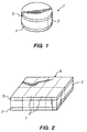
- Figure 1 shows a plan view of an electrical device made by the method of the invention
- the electrical device comprises a resistive element composed of a conductive polymer composition.
- This composition comprises a polymeric component comprising one or more crystalline polymers.
- the polymeric component has a crystallinity of at least 20%, preferably at least 30%, particularly at least 40%, as measured by a differential scanning calorimeter (DSC). It is preferred that the polymeric component comprise polyethylene, e.g. high density polyethylene, medium density polyethylene, low density polyethylene, or linear low density polyethylene; an ethylene copolymer or terpolymer, e.g.
- EAA ethylene/acrylic acid copolymer
- EAA ethylene/ethyl acrylate
- EBA ethylene/butyl acrylate
- PVDF polyvinylidene fluoride
- High density polyethylene that has a density of at least 0.94 g/cm 3 , generally 0.95 to 0.97 g/cm 3 , is particularly preferred.
- additional polymers e.g.
- the polymeric component generally comprises 40 to 80% by volume, preferably 45 to 75% by volume, particularly 50 to 70% by volume of the total volume of the composition.
- the polymeric component comprise at most 70% by volume, preferably at most 66% by volume, particularly at most 64% by volume, especially at most 62% by volume of the total volume of the composition.
- the polymeric component has a melting temperature, as measured by the peak of the endotherm of a differential scanning calorimeter, of T m .
- T m is defined as the temperature of the highest temperature peak.
- a particulate conductive filler Dispersed in the polymeric component is a particulate conductive filler.
- Suitable conductive fillers include carbon black, graphite, metal, e.g. nickel, metal oxide, conductive coated glass or ceramic beads, particulate conductive polymer, or a combination of these.
- Such particulate conductive fillers may be in the form of powder, beads, flakes, or fibers.
- the conductive filler comprise carbon black, and for compositions used in circuit protection devices it is particularly preferred that the carbon black have a DBP number of 60 to 120 cm 3 /100g, preferably 60 to 100 cm 3 /100g, particularly 60 to 90 cm 3 /100g, especially 65 to 85 cm 3 /100g.
- the DBP number is an indication of the amount of structure of the carbon black and is determined by the volume of n-dibutyl phthalate (DBP) absorbed by a unit mass of carbon black. This test is described in ASTM D2414-93.
- the quantity of conductive filler needed is based on the required resistivity of the composition and the resistivity of the conductive filler itself.
- the particulate conductive filler comprises 20 to 60% by volume, preferably 25 to 55% by volume, particularly 30 to 50% by volume of the total composition.
- the conductive filler preferably comprises at least 30% by volume, particularly at least 34% by volume, especially at least 36% by volume, most especially at least 38% by volume of the total volume of the composition.
- the conductive polymer composition may comprise additional components including antioxidants, inert fillers, nonconductive fillers, radiation crosslinking agents (often referred to as prorads or crosslinking enhancers), stabilizers, dispersing agents, coupling agents, acid scavengers (e.g. CaCO 3 ), or other components. These components generally comprise at most 20% by volume of the total composition.
- the composition exhibits positive temperature coefficient (PTC) behavior, i.e. it shows a sharp increase in resistivity with temperature over a relatively small temperature range.
- PTC positive temperature coefficient
- the term "PTC” is used to mean a composition or device that has an R 14 value of at least 2.5 and/or an R 100 value of at least 10, and it is preferred that the composition or device should have an R 30 value of at least 6, where R 14 is the ratio of the resistivities at the end and the beginning of a 14°C range, R 100 is the ratio of the resistivities at the end and the beginning of a 100°C range, and R 30 is the ratio of the resistivities at the end and the beginning of a 30°C range.
- compositions used for devices of the invention show a PTC anomaly over the range from 20°C to (T m + 5°C) of at least 10 4 , preferably at least 10 4.5 , particularly at least 10 5 , especially at least 10 5.5 , i.e. the log[(resistance at (T m + 5°C)/resistance at 20°C] is at least 4.0, preferably at least 4.5, particularly at least 5.0, especially at least 5.5. If the maximum resistance is achieved at a temperature T x that is below (T m + 5°C), the PTC anomaly is determined by the log(resistance at T x /resistance at 20°C). In order to ensure that effects of processing and thermal history are neutralized, at least one thermal cycle from 20°C to (T m + 5°C) and back to 20°C should be conducted before the PTC anomaly is measured.
- composition be melt-processed using melt-processing equipment including mixers made by such manufacturers as Brabender, Moriyama, and Banbury, and continuous compounding equipment, such as co- and counter-rotating twin screw extruders.
- melt-processing equipment including mixers made by such manufacturers as Brabender, Moriyama, and Banbury, and continuous compounding equipment, such as co- and counter-rotating twin screw extruders.
- the components of the composition can be blended in a blender such as a HenschelTM blender to improve the uniformity of the mixture loaded into the mixing equipment.
- the composition can be prepared by using a single melt-mixing step, but it is often advantageous to prepare it by a method in which there are two or more mixing steps, as described in U.S. Application No.
- ohm-cm less than 10 ohm-cm, preferably less than 5 ohm-cm, particularly less than 1 ohm-cm, while maintaining a suitably high PTC anomaly, i.e. at least 4 decades, preferably at least 4.5 decades.
- the composition can be melt-shaped by any suitable method, e.g. melt-extrusion, injection-molding, compression-molding, and sintering, in order to produce a resistive element.
- the element may be of any shape, e.g. rectangular, square, circular, or annular.
- the resistive element has a thickness of at most 0.51 mm (0.020 inch), preferably at most 0.38 mm (0.015 inch), particularly at most 0.25 mm (0.010 inch), especially at most 0.18 mm (0.007 inch).
- the electrical devices may comprise circuit protection devices, heaters, sensors, or resistors in which the resistive element is in physical and electrical contact with at least one electrode that is suitable for connecting the element to a source of electrical power.
- the type of electrode is dependent on the shape of the element, and may be, for example, solid or stranded wires, metal foils, metal meshes, or metallic ink layers.
- the electrical devices can have any shape, e.g. planar, axial, or dogbone, but particularly useful devices comprise two laminar electrodes, preferably metal foil electrodes, with the conductive polymer resistive element sandwiched between them.
- Particularly suitable foil electrodes have at least one surface that is electrodeposited, preferably electrodeposited nickel or copper. Appropriate electrodes are disclosed in U.S.
- Patents Nos. 4,689,475 (Matthiesen), 4,800,253 (Kleiner et al), and International Application No. PCT/US95/07888 (Raychem Corporation, filed June 7, 1995).
- the electrodes may be attached to the resistive element by compression-molding, nip-lamination, or any other appropriate technique.
- Additional metal leads e.g. in the form of wires or straps, can be attached to the foil electrodes to allow electrical connection to a circuit.
- elements to control the thermal output of the device e.g. one or more conductive terminals, can be used. These terminals can be in the form of metal plates, e.g.
- crosslinking can be accomplished by chemical means or by irradiation, e.g. using an electron beam or a Co 60 ⁇ irradiation source.
- the level of crosslinking depends on the required application for the composition, but is generally less than the equivalent of 200 Mrads, and is preferably substantially less, i.e. from 1 to 20 Mrads, preferably from 1 to 15 Mrads, particularly from 2 to 10 Mrads for low voltage (i.e. less than 60 volts) applications.
- Useful circuit protection devices for applications of less than 30 volts can be made by irradiating the device to at least 2 Mrads but at most 10 Mrads.
- the device is cut from a laminate comprising the conductive polymer composition positioned between two metal foils, the device is exposed to a thermal treatment before crosslinking of the conductive polymer composition is done.
- the device is first cut from the laminate in a cutting step.
- cutting is used to include any method of isolating or separating the resistive element of the device from the laminate, e.g. dicing, punching, shearing, cutting, etching and/or breaking as described in International Application No. PCT/US95/07420 (Raychem Corporation, filed June 8, 1995).
- the thermal treatment requires that the device be subjected to a temperature T t that is greater than T m , preferably at least (T m + 20°C), particularly at least (T m + 50°C), especially at least (T m + 70°C).
- the duration of the thermal exposure may be very short, but is sufficient so that the entire conductive polymer in the resistive element reaches a temperature of at least (T m + 5°C).
- the thermal exposure at T t is at least 0.5 seconds, preferably at least 1.0 second, particularly at least 1.5 seconds, especially at least 2.0 seconds.
- a suitable thermal treatment for devices made from high density polyethylene or ethylene/butyl acrylate copolymer may be achieved by dipping the device into a solder bath heated to a temperature of about 240 to 245°C, i.e. at least 100°C above T m , for a period of 1.5 to 2.5 seconds.
- good results have been achieved by passing the devices through an oven on a belt and exposing them to a temperature at least 100°C above T m for 3 seconds.
- electrical leads can be attached to the electrodes by means of solder.
- the device After exposure to the thermal treatment, the device is cooled to a temperature below T m , i.e. to a temperature of at most (T m - 30°C), preferably at most (T m - 50°C), especially at most (T m - 70°C). It is particularly preferred that the device be cooled to a temperature at which the conductive polymer composition has achieved 90% of it maximum crystallization. Cooling to room temperature, particularly to 20°C, is particularly preferred. The cooled device is then crosslinked, preferably by irradiation.
- the devices are preferably circuit protection devices that generally have a resistance at 20°C, R 20 , of less than 100 ohms, preferably less than 20 ohms, particularly less than 10 ohms, especially less than 5 ohms, most especially less than 1 ohm. It is particularly preferred that the device have a resistance of at most 1.0 ohm, preferably at most 0.50 ohm, especially at most 0.10 ohm, e.g. 0.001 to 0.100 ohm. The resistance is measured after one thermal cycle from 20°C to (T m + 5°C) to 20°C. Heaters generally have a resistance of at least 100 ohms, preferably at least 250 ohms, particularly at least 500 ohms.
- the device When in the form of a circuit protection device, the device has a resistivity at 20°C, ⁇ 20 , of at most 10 ohm-cm, preferably at most 2.0 ohm-cm, particularly at most 1.5 ohm-cm, more particularly at most 1.0 ohm-cm, especially at most 0.9 ohm-cm, most especially at most 0.8 ohm-cm.
- the electrical device is a heater
- the resistivity of the conductive polymer composition is generally substantially higher than for circuit protection devices, e.g. 10 2 to 10 5 ohm-cm, preferably 10 2 to 10 4 ohm-cm.
- Devices made by the method of the invention show improvement in PTC anomaly over devices prepared by conventional methods in which the laminate is crosslinked before the device is cut.
- a standard device is one made from the same composition as a device of the invention and following the same procedure, except that, for the standard device, the laminate was crosslinked before the cutting step.
- the resistivity ⁇ 20 for a device made by the method of the invention is less than 1.20 ⁇ 20c , preferably less than 1.15 ⁇ 20c , especially less than 1.10 ⁇ 20c , wherein ⁇ 20c is the resistivity at 20°C for a standard device measured following one thermal cycle from 20°C to (T m + 5°C) to 20°C.
- the PTC anomaly for a device of the invention is at least 1.15PTC c , preferably at least 1.20PTC c , particularly at least 1.25PTC c , especially at least 1.30PTC c , wherein PTC c is the PTC anomaly from 20°C to (T m + 5°C) for a standard device measured following one thermal cycle from 20°C to (T m + 5°C) to 20°C.
- devices made by the method of the invention have more than a 40% increase in PTC anomaly height with a relatively small, i.e. less than 20%, increase in resistivity at 20°C.
- the difference in resistivity for ⁇ 20 , ⁇ 20 is determined from the formula [( ⁇ 20 for a device of the invention - ⁇ 20 for a standard device)/( ⁇ 20 for a device of the invention)].
- the improvement for the PTC anomaly, ⁇ PTC is determined from the formula [(PTC for a device made by the method of the invention - PTC for a standard device)/(PTC for a device made by the method of the invention)].
- Devices of the invention also show improvement in performance in electrical tests such as cycle life, i.e. the stability of the device over time when subjected to a series of electrical tests that convert the device into a high resistance, high temperature state, and trip endurance, i.e. the stability of the device over time when powered into a high resistance, high temperature state.
- cycle life i.e. the stability of the device over time when subjected to a series of electrical tests that convert the device into a high resistance, high temperature state
- trip endurance i.e. the stability of the device over time when powered into a high resistance, high temperature state.
- FIG. 1 shows an electrical device 1 made by the method of the invention.
- Resistive element 3 composed of a conductive polymer composition, is sandwiched between two metal foil electrodes 5,7.
- Figure 2 shows laminate 9 in which conductive polymer composition 3 is laminated to first and second metal foil electrodes 5,7. Individual electrical devices 1 can be cut or punched from laminate 9 along the dotted lines.
- Example 1 The invention is illustrated by the following examples, in which Example 1 and those devices prepared by Processes A, C, E, and G are comparative examples.
- the mixture was then compression-molded to give a sheet with a thickness of 0.18 mm (0.007 inch).
- the sheet was laminated between two layers of electrodeposited nickel foil having a thickness of about 0.033 mm (0.0013 inch) (available from Fukuda) by using a press set at 200°C.
- the laminate was irradiated to 10 Mrads using a 3.0 MeV electron beam, and chips with a diameter of 12.7 mm (0.5 inch) were punched from the laminate.
- Devices were formed from each chip by soldering 20 AWG tin-coated copper leads to each metal foil by dipping the chips into a solder formulation of 63% lead/37% tin heated to 245°C for about 2.0 to 3.0 seconds, and allowing the devices to air cool.
- a ferric chloride etch was used to remove the metal foil either from the center 6.25 mm (0.25 inch)-diameter section or from the outer 3.175 mm (0.125 inch) perimeter.
- the resistance versus temperature properties of the devices were determined by positioning the devices in an oven and measuring the resistance at intervals over the temperature range 20 to 160 to 20°C. Two temperature cycles were run.
- the height of the PTC anomaly was determined as log(resistance at 140°C/resistance at 20°C) for the second cycle, and was recorded as PTC 2 . The results are shown in Table I.
- Devices were prepared according to the procedure of Example 1 except that chips were punched from the laminate and leads were attached by solder dipping prior to irradiating the devices to 10 Mrads. Results, as shown in Table I, indicate that devices that were soldered before irradiation, and that were exposed to a temperature during soldering that was higher than the melting temperature of the polymer, had higher PTC anomalies at both the center and edge regions.
- the laminate was irradiated to 10 Mrads using a 3.0 MeV electron beam, and chips with a diameter of 12.7 mm (0.5 inch) were punched from the laminate.
- Devices were formed from each chip by soldering 20 AWG tin-coated copper leads to each metal foil by dipping the chips into a solder formulation of 63% lead/37% tin heated to 245°C for about 3.0 seconds, and allowing the devices to air cool.
- Chips with a diameter of 12.7 mm (0.5 inch) were punched from the laminate and leads were attached to form a device by soldering 20 AWG tin-coated copper leads to each metal foil. Soldering was conducted by dipping the chips into a solder formulation of 63% lead/37% tin heated to 245°C for about 3.0 seconds, and allowing the devices to air cool. The devices were then irradiated to 10 Mrads using a 3.0 MeV electron beam.
- Laminates of different thicknesses were prepared following the process of Example 1.
- Devices were prepared according to Process A or B.
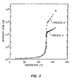
- Figure 3 shows the resistivity versus temperature curve for devices of Example 6 prepared by the conventional Process A, and by Process B, the process of the invention.
- Example Thickness (mm) Process A Process B ⁇ 20 (%) ⁇ PTC (%) ⁇ 20 ( ⁇ -cm) PTC (decades) ⁇ 20 ( ⁇ -cm) PTC (decades) 4 0.33 1.17 6.9 1.46 9.5 19.9 27.4 5 0.66 0.75 5.7 0.83 7.4 9.6 23.0 6 0.17 1.33 4.1 1.43 6.8 7.0 39.7 7 0.33 1.30 7.1 1.40 8.5 7.1 16.5 8 0.53 1.50 9.0 1.53 8.9 2.0 -1.1 9 0.91 1.54 8.3 1.66 8.5 7.2 2.4 10 0.18 0.75 3.6 0.71 6.5 -5.6 44.6 11 0.25 0.76 4.1 0.75 8.6 -1.3 52.3 12 0.51 0.75 5.4 0.83 9.8 9.6 44.9 13 0.14 0.70 3.1 0.80 5.7 1
- the effect of exposing devices containing different amounts of carbon black to a thermal treatment was determined by preblending powdered Petrothene LB832 (HDPE) in a Henschel blender with Raven 430 in the amounts shown by volume percent in Table III. The blend was then mixed using a 70 mm (2.75 inch) Buss kneader to form pellets.
- the pellets of Example 20 were passed through the Buss kneader a second time.
- the pellets of Example 21 were passed through the Buss kneader a third time.
- the total amount of work used during the compounding process i.e. the specific energy consumption (SEC) in MJ/kg, was recorded.
- SEC specific energy consumption
- the pellets for each composition were extruded through a sheet die to give a sheet with a thickness of 0.25 mm (0.010 inch).
- the extruded sheet was laminated as in Example 1.
- Devices were then prepared by either Process C (a conventional process) or D (a process of the invention).
- the laminate was irradiated to 5 Mrads using a 3.0 MeV electron beam, and chips with a diameter of 12.7 mm (0.5 inch) were punched from the laminate.
- Devices were formed from each chip by soldering 20 AWG tin-coated copper leads to each metal foil by dipping the chips into a solder formulation of 63% lead/37% tin heated to 245°C for about 1.5 seconds, and allowing the devices to air cool.
- Chips with a diameter of 12.7 mm (0.5 inch) were punched from the laminate and leads were attached to form a device by soldering 20 AWG tin-coated copper leads to each metal foil. Soldering was conducted by dipping the chips into a solder formulation of 63% lead/37% tin heated to 245°C for about 1.5 seconds, and allowing the devices to air cool. The devices were then irradiated to 5 Mrads using a 3.0 MeV electron beam.
- the resistance versus temperature properties of the devices were determined by following the procedure of Example 1. Resistivity values were calculated from the recorded resistance at 20°C on the first and second cycles, ⁇ 1 and ⁇ 2 , respectively. The height of the PTC anomaly was determined as log(resistance at 140°C/resistance at 20°C) for the first and second cycles, and was recorded in decades as PTC 1 and PTC 2 , respectively. Also calculated were the difference between the resistivity value and the PTC anomaly for devices prepared by Process C and Process D for both the first and second cycles. The difference for the resistivity at 20°C for the first cycle, ⁇ ⁇ 1 , was determined from the formula [(p, for Process D - p, for Process C)/( ⁇ 1 for Process D)].
- the difference for the resistivity at 20°C for the second cycle, ⁇ ⁇ 2 was determined from the formula [( ⁇ 2 for Process D - ⁇ 2 for Process C)/( ⁇ 1 for Process D)].
- the difference for the PTC anomaly for the first cycle, ⁇ PTC 1 was determined from the formula [(PTC 1 for Process D - PTC 1 for Process C)/(PTC 1 for Process D)].
- the difference for the PTC anomaly for the second cycle, ⁇ PTC 2 was determined from the formula [(PTC 2 for Process D - PTC 2 for Process C)/(PTC 2 for Process D)].
- Example 16 17 18 19 20 21 22 CB (Vol%) 32 34 36 38 40 40 40 40 HDPE (Vol%) 68 66 64 62 60 60 60 SEC (MJ/kg) 2.52 2.48 3.06 3.31 3.64 6.01 8.96 Process C ⁇ 1 (ohm-cm) 2.02 1.27 0.98 0.76 0.58 0.65 0.76 PTC 1 (decades) 7.30 6.36 5.81 5.04 3.95 4.89 5.25 ⁇ 2 (ohm-cm) 2.08 1.34 1.02 0.81 0.56 0.67 0.73 PTC 2 (decades) 7.89 6.69 6.19 5.25 4.08 5.09 5.49 Process D ⁇ 1 (ohm-cm) 1.48 1.05 0.83 0.70 0.53 0.63 0.65 PTC 1 (decades) 8.39 7.86 7.38 6.27 4.54 5.79 6.50 ⁇ 2 (ohm-cm) 2.27 1.47 1.09 0.86 0.60 0.71 0.76 PTC 2 (decades) 8.86 8.29 7.65 6.39 4.58 5.95 6.74 ⁇ ⁇ 1
- the laminate was irradiated to 10 Mrads using a 3.0 MeV electron beam, and chips with dimensions of 5.1 x 5.1 mm (0.2 x 0.2 inch) or 20 x 20 mm (0.8 x 0.8 inch) were sheared from the laminate.
- Devices were formed from each chip by soldering 20 AWG tin-coated copper leads to each metal foil by dipping the chips into a solder formulation of 63% lead/37% tin heated to 245°C for about 2.5 seconds, and allowing the devices to air cool.
- the devices were encapsulated by dipping them into HysolTM DK18-05 powdered epoxy, an epoxy resin-anhydride compound available from The Dexter Corporation containing 30 to 60% by weight fused silica, 2% antimony trioxide, 5 to 10% benzophenonetetracarboxylic dianhydride (BTDA), and 30 to 60% bis-A epoxy resin.
- the powder was cured at 155°C for 2 hours.
- the devices were then thermally cycled six times, each cycle being from -40 to 85 to -40°C at a rate of 5°C/minute with a 30 minute dwell at -40°C and 85°C.
- Chips with dimensions of 5.1 x 5.1 mm (0.2 x 0.2 inch) or 20 x 20 mm (0.8 x 0.8 inch) were sheared from the laminate.
- the chips were then heat-treated using a thermal profile in which the temperature increased from 20°C to 240°C in 11 seconds, remained at 240°C for 3 seconds, and then decreased to 20°C over 65 seconds.
- the chips were then irradiated, lead-attached, encapsulated, and thermally cycled as in Process E.
- the resistance versus temperature properties were determined over the range of 20 to 140°C for two cycles.
- the PTC anomaly was determined as log(resistance at 140°C/resistance at 20°C) for both cycles and recorded as PTC 1 for the first cycle and PTC 2 for the second cycle.
- the results, shown in Table IV. indicate that the devices made by the conventional process had substantially less PTC anomaly than those made by the process of the invention.
- the electrical stability was determined by testing for cycle life and trip endurance, described below. The results indicated that, in general, the devices made by the process of the invention had improved resistance stability.
- Devices were tested in a circuit consisting of the device in series with a switch, a DC power supply of either 16 volts or 30 volts, and a fixed resistor that limited the initial current to 40A. The device was tripped into the high resistance state and removed periodically. After each interval, the device was allowed to cool for one hour and the resistance at 20°C was measured. The normalized resistance, R N , was reported.
- Example 23 24 25 26 Size (mm) 5.1 x 5.1 5.1 x 5.1 20 x 20 20 x 20 Process E F E F Resistance (mohms) 70.9 82.1 4.41 4.77 PTC 1 (decades) 5.0 7.2 5.1 7.2 PTC 2 (decades) 4.9 7.5 5.1 7.4 Cycle Life
- R N 16V 100 cycles 1.07 1.00 1.10 1.02 500 cycles 3.04 1.30 1.11 1.00 1000 cycles 3.31 2.00 1.16 1.00 2000 cycles 5.34 3.84 1.28 1.04 24V: 100 cycles 1.15 1.32 1.05 1.00 500 cycles 1.57 1.56 1.07 0.96 1000 cycles 2.20 2.12 1.11 1.04 2000 cycles 3.59 4.18 1.20 1.10 30V: 100 cycles 1.44 1.22 1.09 1.04 500 cycles 1.63 1.10 1.01 1000 cycles 1.81 1.17 1.07 2000 cycles 3.10 1.25 1.11 Trip endurance R N 16V: 5 minutes 1.23 1.22 1.26 1.15 24 hours 1.35 1.21 1.35 1.16 96 hours 1.68 1.45 1.53 1.25 366 hours 2.78 2.
- the laminate was irradiated to 10 Mrads using a 3.0 MeV electron beam and chips with dimensions of 5.1 x 12.1 x 0.23 mm (0.2 x 0.475 x 0.009 inch) were cut from the laminate.
- Devices were formed by soldering 20 AWG leads as in Process E.
- Device resistance at 20°C was 0.071 ohms.
- Chips with dimensions of 5.1 x 12.1 x 0.23 mm (0.2 x 0.475 x 0.009 inch) were cut from the laminate.
- Leads were attached as in Process E and the devices were then heat-treated by exposure to 290°C in a reflow oven for about 3.5 seconds. After cooling to room temperature, the devices were irradiated to 10 Mrads using a 3 MeV electron beam. Device resistance at 20°C was 0.096 ohms.
- Figure 4 shows a curve of the resistance in ohms as a function of temperature for Examples 27 and 28. It is apparent that a device made by the process of the invention has substantially higher PTC anomaly than a device made by a conventional processes.
Landscapes
- Engineering & Computer Science (AREA)
- Microelectronics & Electronic Packaging (AREA)
- Ceramic Engineering (AREA)
- Physics & Mathematics (AREA)
- Electromagnetism (AREA)
- Chemical & Material Sciences (AREA)
- Dispersion Chemistry (AREA)
- Thermistors And Varistors (AREA)
- Apparatuses And Processes For Manufacturing Resistors (AREA)
- Control And Other Processes For Unpacking Of Materials (AREA)
- Surgical Instruments (AREA)
- Beans For Foods Or Fodder (AREA)
Abstract
Description
- (a) preparing a laminate comprising the conductive polymer composition positioned between two metal foils,
- (b) cutting a device from the laminate,
- (c) exposing the device to a thermal treatment at a temperature Tt which is greater than Tm,
- (d) cooling the device, and
- (e) crosslinking the device.
| Example | Process | PTC 2 Center (decades) | PTC 2 Edge (decades) |
| 1 | Irradiate/Punch/Solder | 5.0 | 4.7 |
| 2 | Punch/Solder/Irradiate | 6.0 | 6.0 |
| 3 | Punch/Solder/Irradiate/Punch | 6.3 | 3.4 |
| Example | Thickness (mm) | Process A | Process B | Δρ 20 (%) | ΔPTC (%) | ||
| ρ 20 (Ω-cm) | PTC (decades) | ρ 20 (Ω-cm) | PTC (decades) | ||||
| 4 | 0.33 | 1.17 | 6.9 | 1.46 | 9.5 | 19.9 | 27.4 |
| 5 | 0.66 | 0.75 | 5.7 | 0.83 | 7.4 | 9.6 | 23.0 |
| 6 | 0.17 | 1.33 | 4.1 | 1.43 | 6.8 | 7.0 | 39.7 |
| 7 | 0.33 | 1.30 | 7.1 | 1.40 | 8.5 | 7.1 | 16.5 |
| 8 | 0.53 | 1.50 | 9.0 | 1.53 | 8.9 | 2.0 | -1.1 |
| 9 | 0.91 | 1.54 | 8.3 | 1.66 | 8.5 | 7.2 | 2.4 |
| 10 | 0.18 | 0.75 | 3.6 | 0.71 | 6.5 | -5.6 | 44.6 |
| 11 | 0.25 | 0.76 | 4.1 | 0.75 | 8.6 | -1.3 | 52.3 |
| 12 | 0.51 | 0.75 | 5.4 | 0.83 | 9.8 | 9.6 | 44.9 |
| 13 | 0.14 | 0.70 | 3.1 | 0.80 | 5.7 | 12.5 | 45.6 |
| 14 | 0.30 | 0.66 | 4.5 | 0.75 | 7.1 | 12.0 | 36.6 |
| 15 | 0.53 | 0.64 | 4.4 | 0.76 | 5.9 | 15.8 | 25.4 |
| Example | 16 | 17 | 18 | 19 | 20 | 21 | 22 |
| CB (Vol%) | 32 | 34 | 36 | 38 | 40 | 40 | 40 |
| HDPE (Vol%) | 68 | 66 | 64 | 62 | 60 | 60 | 60 |
| SEC (MJ/kg) | 2.52 | 2.48 | 3.06 | 3.31 | 3.64 | 6.01 | 8.96 |
| Process C | |||||||
| ρ1 (ohm-cm) | 2.02 | 1.27 | 0.98 | 0.76 | 0.58 | 0.65 | 0.76 |
| PTC1 (decades) | 7.30 | 6.36 | 5.81 | 5.04 | 3.95 | 4.89 | 5.25 |
| ρ2 (ohm-cm) | 2.08 | 1.34 | 1.02 | 0.81 | 0.56 | 0.67 | 0.73 |
| PTC2 (decades) | 7.89 | 6.69 | 6.19 | 5.25 | 4.08 | 5.09 | 5.49 |
| Process D | |||||||
| ρ1 (ohm-cm) | 1.48 | 1.05 | 0.83 | 0.70 | 0.53 | 0.63 | 0.65 |
| PTC1 (decades) | 8.39 | 7.86 | 7.38 | 6.27 | 4.54 | 5.79 | 6.50 |
| ρ2 (ohm-cm) | 2.27 | 1.47 | 1.09 | 0.86 | 0.60 | 0.71 | 0.76 |
| PTC2 (decades) | 8.86 | 8.29 | 7.65 | 6.39 | 4.58 | 5.95 | 6.74 |
| Δ ρ1 (%) | -36.4 | -21.0 | -18.1 | -8.6 | -9.4 | -3.2 | -16.9 |
| Δ PTC1 (%) | 13.0 | 19.1 | 21.2 | 19.6 | 13.0 | 15.5 | 19.2 |
| Δ ρ2 (%) | 8.4 | 8.8 | 6.4 | 5.8 | 6.7 | 5.6 | 3.9 |
| Δ PTC2 (%) | 10.9 | 19.3 | 19.1 | 17.8 | 10.9 | 14.5 | 18.5 |
| Example | 23 | 24 | 25 | 26 |
| Size (mm) | 5.1 x 5.1 | 5.1 x 5.1 | 20 x 20 | 20 x 20 |
| Process | E | F | E | F |
| Resistance (mohms) | 70.9 | 82.1 | 4.41 | 4.77 |
| PTC1 (decades) | 5.0 | 7.2 | 5.1 | 7.2 |
| PTC2 (decades) | 4.9 | 7.5 | 5.1 | 7.4 |
| Cycle Life RN | ||||
| 16V: 100 cycles | 1.07 | 1.00 | 1.10 | 1.02 |
| 500 cycles | 3.04 | 1.30 | 1.11 | 1.00 |
| 1000 cycles | 3.31 | 2.00 | 1.16 | 1.00 |
| 2000 cycles | 5.34 | 3.84 | 1.28 | 1.04 |
| 24V: 100 cycles | 1.15 | 1.32 | 1.05 | 1.00 |
| 500 cycles | 1.57 | 1.56 | 1.07 | 0.96 |
| 1000 cycles | 2.20 | 2.12 | 1.11 | 1.04 |
| 2000 cycles | 3.59 | 4.18 | 1.20 | 1.10 |
| 30V: 100 cycles | 1.44 | 1.22 | 1.09 | 1.04 |
| 500 cycles | 1.63 | 1.10 | 1.01 | |
| 1000 cycles | 1.81 | 1.17 | 1.07 | |
| 2000 cycles | 3.10 | 1.25 | 1.11 | |
| Trip endurance RN | ||||
| 16V: 5 minutes | 1.23 | 1.22 | 1.26 | 1.15 |
| 24 hours | 1.35 | 1.21 | 1.35 | 1.16 |
| 96 hours | 1.68 | 1.45 | 1.53 | 1.25 |
| 366 hours | 2.78 | 2.31 | 2.00 | 1.57 |
| 723 hours | 4.23 | 3.39 | 2.71 | 1.89 |
| 30V: 5 minutes | 1.31 | 1.26 | 1.34 | 1.16 |
| 24 hours | 2.04 | 1.32 | 1.60 | 1.24 |
| 96 hours | 2.59 | 1.82 | 1.71 | |
| 366 hours | 10.6 | 3.54 | 2.23 | 1.63 |
| 723 hours | 595 | 7.56 | 2.93 | 1.98 |
Claims (9)
- A method of making an electrical device which comprisessaid method comprising(A) a resistive element which (i) has a thickness of at most 0.51 mm, (ii) is crosslinked to the equivalent of at least 2 Mrads, and (iii) is composed of a conductive polymer composition which comprises(1) a polymeric component having a crystallinity of at least 20% and a melting point Tm, and(2) dispersed in the polymeric component a particulate conductive filler; and(B) two electrodes which (i) are attached to the resistive element, (ii) comprise metal foils, and (iii) can be connected to a source of electrical power,(a) preparing a laminate comprising the conductive polymer composition positioned between two metal foils,(b) cutting a device from the laminate,(c) exposing the device to a thermal treatment at a temperature Tt which is greater than Tm, preferably at least (Tm + 20°C),(d) cooling the device, and(e) crosslinking the device.
- A method according to claim 1 wherein during step (c) electrical leads are attached to the electrodes, preferably by solder.
- A method according to claim 1 wherein crosslinking is achieved by means of irradiation.
- A method according to claim 3 wherein crosslinking is accomplished in a single process.
- A method according to claim 1 wherein the crosslinking level is equivalent to 2 to 10 Mrads.
- A method according to claim 1 wherein the polymeric component comprises polyethylene, an ethylene copolymer, or a fluoropolymer.
- A method according to claim 6 wherein the polymeric component comprises high density polyethylene or ethylene/butyl acrylate copolymer.
- A method according to any one of the preceding claims wherein the conductive filler comprises carbon black.
- A method according to any one of the preceding claims wherein the resistive element has a thickness of at most 0.25 mm.
Applications Claiming Priority (3)
| Application Number | Priority Date | Filing Date | Title |
|---|---|---|---|
| US40876895A | 1995-03-22 | 1995-03-22 | |
| US408768 | 1995-03-22 | ||
| PCT/US1996/003469 WO1996029711A1 (en) | 1995-03-22 | 1996-03-15 | Electrical device |
Publications (2)
| Publication Number | Publication Date |
|---|---|
| EP0815568A1 EP0815568A1 (en) | 1998-01-07 |
| EP0815568B1 true EP0815568B1 (en) | 2005-05-25 |
Family
ID=23617686
Family Applications (1)
| Application Number | Title | Priority Date | Filing Date |
|---|---|---|---|
| EP96911298A Expired - Lifetime EP0815568B1 (en) | 1995-03-22 | 1996-03-15 | Electrical device |
Country Status (9)
| Country | Link |
|---|---|
| US (1) | US6130597A (en) |
| EP (1) | EP0815568B1 (en) |
| JP (1) | JP3930904B2 (en) |
| KR (1) | KR100392572B1 (en) |
| CN (1) | CN1111876C (en) |
| AT (1) | ATE296478T1 (en) |
| CA (1) | CA2215959A1 (en) |
| DE (1) | DE69634777T2 (en) |
| WO (1) | WO1996029711A1 (en) |
Families Citing this family (35)
| Publication number | Priority date | Publication date | Assignee | Title |
|---|---|---|---|---|
| US6202471B1 (en) | 1997-10-10 | 2001-03-20 | Nanomaterials Research Corporation | Low-cost multilaminate sensors |
| US6104587A (en) * | 1997-07-25 | 2000-08-15 | Banich; Ann | Electrical device comprising a conductive polymer |
| WO1999006825A1 (en) * | 1997-07-31 | 1999-02-11 | Nanomaterials Research Corporation | Low-cost multilaminate sensors |
| US6606023B2 (en) | 1998-04-14 | 2003-08-12 | Tyco Electronics Corporation | Electrical devices |
| US6349022B1 (en) | 1998-09-18 | 2002-02-19 | Tyco Electronics Corporation | Latching protection circuit |
| US6137669A (en) * | 1998-10-28 | 2000-10-24 | Chiang; Justin N. | Sensor |
| US6362721B1 (en) * | 1999-08-31 | 2002-03-26 | Tyco Electronics Corporation | Electrical device and assembly |
| US6640420B1 (en) | 1999-09-14 | 2003-11-04 | Tyco Electronics Corporation | Process for manufacturing a composite polymeric circuit protection device |
| US6854176B2 (en) * | 1999-09-14 | 2005-02-15 | Tyco Electronics Corporation | Process for manufacturing a composite polymeric circuit protection device |
| EP1247282A1 (en) * | 2000-01-11 | 2002-10-09 | Tyco Electronics Corporation | Electrical device |
| US6597551B2 (en) | 2000-12-13 | 2003-07-22 | Huladyne Corporation | Polymer current limiting device and method of manufacture |
| JP2002280204A (en) * | 2001-03-19 | 2002-09-27 | Shin Etsu Polymer Co Ltd | Overcurrent protection element |
| JP2002289406A (en) * | 2001-03-26 | 2002-10-04 | Shin Etsu Polymer Co Ltd | Overcurrent protection element |
| KR100890092B1 (en) * | 2001-05-08 | 2009-03-24 | 타이코 일렉트로닉스 레이켐 케이. 케이. | Circuit protection device |
| KR100411778B1 (en) * | 2001-10-12 | 2003-12-24 | 주식회사 쎄라텍 | Manufacturing method for positive temperature coefficent thermistor |
| KR100420470B1 (en) * | 2001-10-31 | 2004-03-02 | 엘지전선 주식회사 | Method of Soldering for Making a PTC Device |
| KR100436581B1 (en) * | 2001-11-10 | 2004-06-19 | 엘지전선 주식회사 | PTC Device Manufacturing Method With Ingredient Of Uniform Specific Property |
| KR100436580B1 (en) * | 2001-11-10 | 2004-06-19 | 엘지전선 주식회사 | PTC Device Manufacturing Method With Ingredient Of Excellent Resistance Repair Specific Property |
| KR100436579B1 (en) * | 2001-11-10 | 2004-06-19 | 엘지전선 주식회사 | PTC Device Manufacturing Method With Excellent Resistance Repair Specific Property And PTC Device Thereof |
| KR100436578B1 (en) * | 2001-11-10 | 2004-06-19 | 엘지전선 주식회사 | PTC Device Manufacturing Method For Lithium Ion Battery Protecting And A PTC Device For Lithium Ion Battery Protecting Thereof |
| TW543041B (en) * | 2001-12-31 | 2003-07-21 | Polytronics Technology Corp | Manufacturing method of over current protection device |
| JP2005535110A (en) * | 2002-06-25 | 2005-11-17 | タイコ・エレクトロニクス・コーポレイション | Integrated devices that provide overcurrent and overvoltage protection and common mode filtering for data bus interfaces |
| US6882520B2 (en) * | 2002-12-03 | 2005-04-19 | Tyco Electronics Raychem K.K. | Solid electrolytic capacitors |
| JP4664905B2 (en) * | 2003-05-02 | 2011-04-06 | タイコ・エレクトロニクス・コーポレイション | Circuit protection device |
| US7701323B1 (en) * | 2003-05-30 | 2010-04-20 | Interconnect Portfolio Llc | Low profile discrete electronic components and applications of same |
| TWI229966B (en) * | 2003-08-27 | 2005-03-21 | Polytronics Technology Corp | Over-current protection device |
| US7920045B2 (en) * | 2004-03-15 | 2011-04-05 | Tyco Electronics Corporation | Surface mountable PPTC device with integral weld plate |
| JP4539141B2 (en) * | 2004-03-31 | 2010-09-08 | Tdk株式会社 | Electrolytic capacitor and manufacturing method thereof |
| WO2006076483A1 (en) * | 2005-01-14 | 2006-07-20 | Tyco Electronics Corporation | Insert injection-compression molding of polymeric ptc electrical devices |
| KR20060103864A (en) | 2005-03-28 | 2006-10-04 | 타이코 일렉트로닉스 코포레이션 | Surface mounted multilayer electrical circuit protection device with active elements between PPTC layers |
| EP1911047B1 (en) * | 2005-07-29 | 2009-04-01 | Tyco Electronics Corporation | Circuit protection device having thermally coupled mov overvoltage element and pptc overcurrent element |
| US7918977B2 (en) | 2005-11-08 | 2011-04-05 | Synkera Technologies, Inc. | Solid state electrochemical gas sensor and method for fabricating same |
| TWI464755B (en) * | 2012-11-29 | 2014-12-11 | Polytronics Technology Corp | Surface mountable over-current protection device |
| US9646746B2 (en) * | 2014-07-11 | 2017-05-09 | Ittelfuse, Inc. | Electrical device |
| CN110911075B (en) * | 2019-12-17 | 2021-11-30 | 深圳市慧瑞电子材料有限公司 | Preparation method of high-molecular thermistor and high-molecular thermistor |
Family Cites Families (28)
| Publication number | Priority date | Publication date | Assignee | Title |
|---|---|---|---|---|
| US4560498A (en) * | 1975-08-04 | 1985-12-24 | Raychem Corporation | Positive temperature coefficient of resistance compositions |
| US4534889A (en) * | 1976-10-15 | 1985-08-13 | Raychem Corporation | PTC Compositions and devices comprising them |
| US4388607A (en) * | 1976-12-16 | 1983-06-14 | Raychem Corporation | Conductive polymer compositions, and to devices comprising such compositions |
| US4200973A (en) * | 1978-08-10 | 1980-05-06 | Samuel Moore And Company | Method of making self-temperature regulating electrical heating cable |
| US4237441A (en) * | 1978-12-01 | 1980-12-02 | Raychem Corporation | Low resistivity PTC compositions |
| US4545926A (en) * | 1980-04-21 | 1985-10-08 | Raychem Corporation | Conductive polymer compositions and devices |
| US5049850A (en) * | 1980-04-21 | 1991-09-17 | Raychem Corporation | Electrically conductive device having improved properties under electrical stress |
| US4591700A (en) * | 1980-05-19 | 1986-05-27 | Raychem Corporation | PTC compositions |
| DE3280447T2 (en) * | 1981-04-02 | 1994-07-14 | Raychem Corp | Crosslinking of PTC-conductive polymers by radiation. |
| US4935156A (en) * | 1981-09-09 | 1990-06-19 | Raychem Corporation | Conductive polymer compositions |
| US4514620A (en) * | 1983-09-22 | 1985-04-30 | Raychem Corporation | Conductive polymers exhibiting PTC characteristics |
| US4774024A (en) * | 1985-03-14 | 1988-09-27 | Raychem Corporation | Conductive polymer compositions |
| US4724417A (en) * | 1985-03-14 | 1988-02-09 | Raychem Corporation | Electrical devices comprising cross-linked conductive polymers |
| US4857880A (en) * | 1985-03-14 | 1989-08-15 | Raychem Corporation | Electrical devices comprising cross-linked conductive polymers |
| US4689475A (en) * | 1985-10-15 | 1987-08-25 | Raychem Corporation | Electrical devices containing conductive polymers |
| JPS62131065A (en) * | 1985-12-03 | 1987-06-13 | Idemitsu Kosan Co Ltd | Polymer composition having positive temperature dependence |
| US4907340A (en) * | 1987-09-30 | 1990-03-13 | Raychem Corporation | Electrical device comprising conductive polymers |
| US5174924A (en) * | 1990-06-04 | 1992-12-29 | Fujikura Ltd. | Ptc conductive polymer composition containing carbon black having large particle size and high dbp absorption |
| US5436609A (en) * | 1990-09-28 | 1995-07-25 | Raychem Corporation | Electrical device |
| US5089801A (en) * | 1990-09-28 | 1992-02-18 | Raychem Corporation | Self-regulating ptc devices having shaped laminar conductive terminals |
| JPH04167501A (en) * | 1990-10-31 | 1992-06-15 | Daito Tsushinki Kk | Ptc element |
| US5250228A (en) * | 1991-11-06 | 1993-10-05 | Raychem Corporation | Conductive polymer composition |
| US5303115A (en) * | 1992-01-27 | 1994-04-12 | Raychem Corporation | PTC circuit protection device comprising mechanical stress riser |
| US5378407A (en) * | 1992-06-05 | 1995-01-03 | Raychem Corporation | Conductive polymer composition |
| DE69333211T2 (en) * | 1992-07-09 | 2004-07-01 | Tyco Electronics Corp. | Electrical components |
| US5451919A (en) * | 1993-06-29 | 1995-09-19 | Raychem Corporation | Electrical device comprising a conductive polymer composition |
| EP0764333B1 (en) * | 1994-06-08 | 1999-12-01 | Raychem Corporation | Electrical devices containing conductive polymers |
| EP0766867B1 (en) * | 1994-06-09 | 2002-11-20 | Tyco Electronics Corporation | Electrical devices |
-
1996
- 1996-03-15 JP JP52849396A patent/JP3930904B2/en not_active Expired - Fee Related
- 1996-03-15 CA CA002215959A patent/CA2215959A1/en not_active Abandoned
- 1996-03-15 EP EP96911298A patent/EP0815568B1/en not_active Expired - Lifetime
- 1996-03-15 CN CN96194060A patent/CN1111876C/en not_active Expired - Lifetime
- 1996-03-15 DE DE69634777T patent/DE69634777T2/en not_active Expired - Fee Related
- 1996-03-15 KR KR1019970706572A patent/KR100392572B1/en not_active Expired - Fee Related
- 1996-03-15 AT AT96911298T patent/ATE296478T1/en not_active IP Right Cessation
- 1996-03-15 WO PCT/US1996/003469 patent/WO1996029711A1/en not_active Ceased
-
1997
- 1997-02-10 US US08/798,887 patent/US6130597A/en not_active Expired - Fee Related
Also Published As
| Publication number | Publication date |
|---|---|
| KR100392572B1 (en) | 2003-10-17 |
| WO1996029711A1 (en) | 1996-09-26 |
| JP3930904B2 (en) | 2007-06-13 |
| EP0815568A1 (en) | 1998-01-07 |
| CA2215959A1 (en) | 1996-09-26 |
| CN1185229A (en) | 1998-06-17 |
| ATE296478T1 (en) | 2005-06-15 |
| DE69634777T2 (en) | 2006-02-02 |
| DE69634777D1 (en) | 2005-06-30 |
| CN1111876C (en) | 2003-06-18 |
| US6130597A (en) | 2000-10-10 |
| KR19980703169A (en) | 1998-10-15 |
| JPH11502374A (en) | 1999-02-23 |
Similar Documents
| Publication | Publication Date | Title |
|---|---|---|
| US6130597A (en) | Method of making an electrical device comprising a conductive polymer | |
| EP0815569B1 (en) | Conductive polymer composition and device | |
| US5451919A (en) | Electrical device comprising a conductive polymer composition | |
| EP0764333B1 (en) | Electrical devices containing conductive polymers | |
| US6104587A (en) | Electrical device comprising a conductive polymer | |
| EP0764187B1 (en) | Conductive polymer composition | |
| EP1091366B1 (en) | Electrical device and assembly | |
| EP1042765B1 (en) | Method of making an electrical device |
Legal Events
| Date | Code | Title | Description |
|---|---|---|---|
| PUAI | Public reference made under article 153(3) epc to a published international application that has entered the european phase |
Free format text: ORIGINAL CODE: 0009012 |
|
| 17P | Request for examination filed |
Effective date: 19970911 |
|
| AK | Designated contracting states |
Kind code of ref document: A1 Designated state(s): AT BE CH DE DK ES FI FR GB IE IT LI NL SE |
|
| 17Q | First examination report despatched |
Effective date: 20040322 |
|
| GRAP | Despatch of communication of intention to grant a patent |
Free format text: ORIGINAL CODE: EPIDOSNIGR1 |
|
| RAP1 | Party data changed (applicant data changed or rights of an application transferred) |
Owner name: TYCO ELECTRONICS CORPORATION |
|
| GRAS | Grant fee paid |
Free format text: ORIGINAL CODE: EPIDOSNIGR3 |
|
| GRAA | (expected) grant |
Free format text: ORIGINAL CODE: 0009210 |
|
| AK | Designated contracting states |
Kind code of ref document: B1 Designated state(s): AT BE CH DE DK ES FI FR GB IE IT LI NL SE |
|
| PG25 | Lapsed in a contracting state [announced via postgrant information from national office to epo] |
Ref country code: NL Free format text: LAPSE BECAUSE OF FAILURE TO SUBMIT A TRANSLATION OF THE DESCRIPTION OR TO PAY THE FEE WITHIN THE PRESCRIBED TIME-LIMIT Effective date: 20050525 Ref country code: LI Free format text: LAPSE BECAUSE OF FAILURE TO SUBMIT A TRANSLATION OF THE DESCRIPTION OR TO PAY THE FEE WITHIN THE PRESCRIBED TIME-LIMIT Effective date: 20050525 Ref country code: IT Free format text: LAPSE BECAUSE OF FAILURE TO SUBMIT A TRANSLATION OF THE DESCRIPTION OR TO PAY THE FEE WITHIN THE PRESCRIBED TIME-LIMIT;WARNING: LAPSES OF ITALIAN PATENTS WITH EFFECTIVE DATE BEFORE 2007 MAY HAVE OCCURRED AT ANY TIME BEFORE 2007. THE CORRECT EFFECTIVE DATE MAY BE DIFFERENT FROM THE ONE RECORDED. Effective date: 20050525 Ref country code: FI Free format text: LAPSE BECAUSE OF FAILURE TO SUBMIT A TRANSLATION OF THE DESCRIPTION OR TO PAY THE FEE WITHIN THE PRESCRIBED TIME-LIMIT Effective date: 20050525 Ref country code: CH Free format text: LAPSE BECAUSE OF FAILURE TO SUBMIT A TRANSLATION OF THE DESCRIPTION OR TO PAY THE FEE WITHIN THE PRESCRIBED TIME-LIMIT Effective date: 20050525 Ref country code: BE Free format text: LAPSE BECAUSE OF FAILURE TO SUBMIT A TRANSLATION OF THE DESCRIPTION OR TO PAY THE FEE WITHIN THE PRESCRIBED TIME-LIMIT Effective date: 20050525 Ref country code: AT Free format text: LAPSE BECAUSE OF FAILURE TO SUBMIT A TRANSLATION OF THE DESCRIPTION OR TO PAY THE FEE WITHIN THE PRESCRIBED TIME-LIMIT Effective date: 20050525 |
|
| REG | Reference to a national code |
Ref country code: GB Ref legal event code: FG4D |
|
| REG | Reference to a national code |
Ref country code: CH Ref legal event code: EP |
|
| REG | Reference to a national code |
Ref country code: IE Ref legal event code: FG4D |
|
| REF | Corresponds to: |
Ref document number: 69634777 Country of ref document: DE Date of ref document: 20050630 Kind code of ref document: P |
|
| PG25 | Lapsed in a contracting state [announced via postgrant information from national office to epo] |
Ref country code: SE Free format text: LAPSE BECAUSE OF FAILURE TO SUBMIT A TRANSLATION OF THE DESCRIPTION OR TO PAY THE FEE WITHIN THE PRESCRIBED TIME-LIMIT Effective date: 20050825 Ref country code: DK Free format text: LAPSE BECAUSE OF FAILURE TO SUBMIT A TRANSLATION OF THE DESCRIPTION OR TO PAY THE FEE WITHIN THE PRESCRIBED TIME-LIMIT Effective date: 20050825 |
|
| PG25 | Lapsed in a contracting state [announced via postgrant information from national office to epo] |
Ref country code: ES Free format text: LAPSE BECAUSE OF FAILURE TO SUBMIT A TRANSLATION OF THE DESCRIPTION OR TO PAY THE FEE WITHIN THE PRESCRIBED TIME-LIMIT Effective date: 20050905 |
|
| REG | Reference to a national code |
Ref country code: CH Ref legal event code: PL |
|
| NLV1 | Nl: lapsed or annulled due to failure to fulfill the requirements of art. 29p and 29m of the patents act | ||
| PG25 | Lapsed in a contracting state [announced via postgrant information from national office to epo] |
Ref country code: IE Free format text: LAPSE BECAUSE OF NON-PAYMENT OF DUE FEES Effective date: 20060315 |
|
| PLBE | No opposition filed within time limit |
Free format text: ORIGINAL CODE: 0009261 |
|
| STAA | Information on the status of an ep patent application or granted ep patent |
Free format text: STATUS: NO OPPOSITION FILED WITHIN TIME LIMIT |
|
| ET | Fr: translation filed | ||
| 26N | No opposition filed |
Effective date: 20060228 |
|
| REG | Reference to a national code |
Ref country code: HK Ref legal event code: WD Ref document number: 1007914 Country of ref document: HK |
|
| REG | Reference to a national code |
Ref country code: IE Ref legal event code: MM4A |
|
| PGFP | Annual fee paid to national office [announced via postgrant information from national office to epo] |
Ref country code: DE Payment date: 20080430 Year of fee payment: 13 |
|
| PG25 | Lapsed in a contracting state [announced via postgrant information from national office to epo] |
Ref country code: DE Free format text: LAPSE BECAUSE OF NON-PAYMENT OF DUE FEES Effective date: 20091001 |
|
| PGFP | Annual fee paid to national office [announced via postgrant information from national office to epo] |
Ref country code: FR Payment date: 20110331 Year of fee payment: 16 |
|
| PGFP | Annual fee paid to national office [announced via postgrant information from national office to epo] |
Ref country code: GB Payment date: 20110325 Year of fee payment: 16 |
|
| GBPC | Gb: european patent ceased through non-payment of renewal fee |
Effective date: 20120315 |
|
| REG | Reference to a national code |
Ref country code: FR Ref legal event code: ST Effective date: 20121130 |
|
| PG25 | Lapsed in a contracting state [announced via postgrant information from national office to epo] |
Ref country code: GB Free format text: LAPSE BECAUSE OF NON-PAYMENT OF DUE FEES Effective date: 20120315 Ref country code: FR Free format text: LAPSE BECAUSE OF NON-PAYMENT OF DUE FEES Effective date: 20120402 |