EP0814510A2 - TAB tape and semiconductor device using the TAB tape - Google Patents
TAB tape and semiconductor device using the TAB tape Download PDFInfo
- Publication number
- EP0814510A2 EP0814510A2 EP97110042A EP97110042A EP0814510A2 EP 0814510 A2 EP0814510 A2 EP 0814510A2 EP 97110042 A EP97110042 A EP 97110042A EP 97110042 A EP97110042 A EP 97110042A EP 0814510 A2 EP0814510 A2 EP 0814510A2
- Authority
- EP
- European Patent Office
- Prior art keywords
- patterns
- dummy
- semiconductor device
- tape
- metallic
- Prior art date
- Legal status (The legal status is an assumption and is not a legal conclusion. Google has not performed a legal analysis and makes no representation as to the accuracy of the status listed.)
- Granted
Links
Images

Classifications
-
- H—ELECTRICITY
- H01—ELECTRIC ELEMENTS
- H01L—SEMICONDUCTOR DEVICES NOT COVERED BY CLASS H10
- H01L24/00—Arrangements for connecting or disconnecting semiconductor or solid-state bodies; Methods or apparatus related thereto
- H01L24/01—Means for bonding being attached to, or being formed on, the surface to be connected, e.g. chip-to-package, die-attach, "first-level" interconnects; Manufacturing methods related thereto
- H01L24/02—Bonding areas ; Manufacturing methods related thereto
-
- H—ELECTRICITY
- H01—ELECTRIC ELEMENTS
- H01L—SEMICONDUCTOR DEVICES NOT COVERED BY CLASS H10
- H01L21/00—Processes or apparatus adapted for the manufacture or treatment of semiconductor or solid state devices or of parts thereof
- H01L21/02—Manufacture or treatment of semiconductor devices or of parts thereof
- H01L21/04—Manufacture or treatment of semiconductor devices or of parts thereof the devices having at least one potential-jump barrier or surface barrier, e.g. PN junction, depletion layer or carrier concentration layer
- H01L21/50—Assembly of semiconductor devices using processes or apparatus not provided for in a single one of the subgroups H01L21/06 - H01L21/326, e.g. sealing of a cap to a base of a container
- H01L21/60—Attaching or detaching leads or other conductive members, to be used for carrying current to or from the device in operation
-
- H—ELECTRICITY
- H01—ELECTRIC ELEMENTS
- H01L—SEMICONDUCTOR DEVICES NOT COVERED BY CLASS H10
- H01L23/00—Details of semiconductor or other solid state devices
- H01L23/48—Arrangements for conducting electric current to or from the solid state body in operation, e.g. leads, terminal arrangements ; Selection of materials therefor
- H01L23/488—Arrangements for conducting electric current to or from the solid state body in operation, e.g. leads, terminal arrangements ; Selection of materials therefor consisting of soldered or bonded constructions
- H01L23/495—Lead-frames or other flat leads
- H01L23/49572—Lead-frames or other flat leads consisting of thin flexible metallic tape with or without a film carrier
-
- H—ELECTRICITY
- H01—ELECTRIC ELEMENTS
- H01L—SEMICONDUCTOR DEVICES NOT COVERED BY CLASS H10
- H01L23/00—Details of semiconductor or other solid state devices
- H01L23/48—Arrangements for conducting electric current to or from the solid state body in operation, e.g. leads, terminal arrangements ; Selection of materials therefor
- H01L23/488—Arrangements for conducting electric current to or from the solid state body in operation, e.g. leads, terminal arrangements ; Selection of materials therefor consisting of soldered or bonded constructions
- H01L23/498—Leads, i.e. metallisations or lead-frames on insulating substrates, e.g. chip carriers
- H01L23/4985—Flexible insulating substrates
-
- H—ELECTRICITY
- H05—ELECTRIC TECHNIQUES NOT OTHERWISE PROVIDED FOR
- H05K—PRINTED CIRCUITS; CASINGS OR CONSTRUCTIONAL DETAILS OF ELECTRIC APPARATUS; MANUFACTURE OF ASSEMBLAGES OF ELECTRICAL COMPONENTS
- H05K3/00—Apparatus or processes for manufacturing printed circuits
- H05K3/30—Assembling printed circuits with electric components, e.g. with resistor
- H05K3/32—Assembling printed circuits with electric components, e.g. with resistor electrically connecting electric components or wires to printed circuits
- H05K3/34—Assembling printed circuits with electric components, e.g. with resistor electrically connecting electric components or wires to printed circuits by soldering
- H05K3/3452—Solder masks
-
- H—ELECTRICITY
- H01—ELECTRIC ELEMENTS
- H01L—SEMICONDUCTOR DEVICES NOT COVERED BY CLASS H10
- H01L2224/00—Indexing scheme for arrangements for connecting or disconnecting semiconductor or solid-state bodies and methods related thereto as covered by H01L24/00
- H01L2224/01—Means for bonding being attached to, or being formed on, the surface to be connected, e.g. chip-to-package, die-attach, "first-level" interconnects; Manufacturing methods related thereto
- H01L2224/02—Bonding areas; Manufacturing methods related thereto
- H01L2224/04—Structure, shape, material or disposition of the bonding areas prior to the connecting process
- H01L2224/0401—Bonding areas specifically adapted for bump connectors, e.g. under bump metallisation [UBM]
-
- H—ELECTRICITY
- H01—ELECTRIC ELEMENTS
- H01L—SEMICONDUCTOR DEVICES NOT COVERED BY CLASS H10
- H01L24/00—Arrangements for connecting or disconnecting semiconductor or solid-state bodies; Methods or apparatus related thereto
- H01L24/01—Means for bonding being attached to, or being formed on, the surface to be connected, e.g. chip-to-package, die-attach, "first-level" interconnects; Manufacturing methods related thereto
- H01L24/10—Bump connectors ; Manufacturing methods related thereto
- H01L24/15—Structure, shape, material or disposition of the bump connectors after the connecting process
- H01L24/16—Structure, shape, material or disposition of the bump connectors after the connecting process of an individual bump connector
-
- H—ELECTRICITY
- H01—ELECTRIC ELEMENTS
- H01L—SEMICONDUCTOR DEVICES NOT COVERED BY CLASS H10
- H01L2924/00—Indexing scheme for arrangements or methods for connecting or disconnecting semiconductor or solid-state bodies as covered by H01L24/00
- H01L2924/01—Chemical elements
- H01L2924/01004—Beryllium [Be]
-
- H—ELECTRICITY
- H01—ELECTRIC ELEMENTS
- H01L—SEMICONDUCTOR DEVICES NOT COVERED BY CLASS H10
- H01L2924/00—Indexing scheme for arrangements or methods for connecting or disconnecting semiconductor or solid-state bodies as covered by H01L24/00
- H01L2924/01—Chemical elements
- H01L2924/01029—Copper [Cu]
-
- H—ELECTRICITY
- H01—ELECTRIC ELEMENTS
- H01L—SEMICONDUCTOR DEVICES NOT COVERED BY CLASS H10
- H01L2924/00—Indexing scheme for arrangements or methods for connecting or disconnecting semiconductor or solid-state bodies as covered by H01L24/00
- H01L2924/01—Chemical elements
- H01L2924/01033—Arsenic [As]
-
- H—ELECTRICITY
- H01—ELECTRIC ELEMENTS
- H01L—SEMICONDUCTOR DEVICES NOT COVERED BY CLASS H10
- H01L2924/00—Indexing scheme for arrangements or methods for connecting or disconnecting semiconductor or solid-state bodies as covered by H01L24/00
- H01L2924/01—Chemical elements
- H01L2924/01082—Lead [Pb]
-
- H—ELECTRICITY
- H01—ELECTRIC ELEMENTS
- H01L—SEMICONDUCTOR DEVICES NOT COVERED BY CLASS H10
- H01L2924/00—Indexing scheme for arrangements or methods for connecting or disconnecting semiconductor or solid-state bodies as covered by H01L24/00
- H01L2924/013—Alloys
- H01L2924/014—Solder alloys
-
- H—ELECTRICITY
- H01—ELECTRIC ELEMENTS
- H01L—SEMICONDUCTOR DEVICES NOT COVERED BY CLASS H10
- H01L2924/00—Indexing scheme for arrangements or methods for connecting or disconnecting semiconductor or solid-state bodies as covered by H01L24/00
- H01L2924/10—Details of semiconductor or other solid state devices to be connected
- H01L2924/11—Device type
- H01L2924/14—Integrated circuits
-
- H—ELECTRICITY
- H01—ELECTRIC ELEMENTS
- H01L—SEMICONDUCTOR DEVICES NOT COVERED BY CLASS H10
- H01L2924/00—Indexing scheme for arrangements or methods for connecting or disconnecting semiconductor or solid-state bodies as covered by H01L24/00
- H01L2924/15—Details of package parts other than the semiconductor or other solid state devices to be connected
- H01L2924/151—Die mounting substrate
- H01L2924/1517—Multilayer substrate
- H01L2924/15172—Fan-out arrangement of the internal vias
- H01L2924/15173—Fan-out arrangement of the internal vias in a single layer of the multilayer substrate
-
- H—ELECTRICITY
- H01—ELECTRIC ELEMENTS
- H01L—SEMICONDUCTOR DEVICES NOT COVERED BY CLASS H10
- H01L2924/00—Indexing scheme for arrangements or methods for connecting or disconnecting semiconductor or solid-state bodies as covered by H01L24/00
- H01L2924/15—Details of package parts other than the semiconductor or other solid state devices to be connected
- H01L2924/151—Die mounting substrate
- H01L2924/153—Connection portion
- H01L2924/1531—Connection portion the connection portion being formed only on the surface of the substrate opposite to the die mounting surface
- H01L2924/15311—Connection portion the connection portion being formed only on the surface of the substrate opposite to the die mounting surface being a ball array, e.g. BGA
-
- H—ELECTRICITY
- H05—ELECTRIC TECHNIQUES NOT OTHERWISE PROVIDED FOR
- H05K—PRINTED CIRCUITS; CASINGS OR CONSTRUCTIONAL DETAILS OF ELECTRIC APPARATUS; MANUFACTURE OF ASSEMBLAGES OF ELECTRICAL COMPONENTS
- H05K1/00—Printed circuits
- H05K1/02—Details
- H05K1/03—Use of materials for the substrate
- H05K1/0393—Flexible materials
-
- H—ELECTRICITY
- H05—ELECTRIC TECHNIQUES NOT OTHERWISE PROVIDED FOR
- H05K—PRINTED CIRCUITS; CASINGS OR CONSTRUCTIONAL DETAILS OF ELECTRIC APPARATUS; MANUFACTURE OF ASSEMBLAGES OF ELECTRICAL COMPONENTS
- H05K2201/00—Indexing scheme relating to printed circuits covered by H05K1/00
- H05K2201/09—Shape and layout
- H05K2201/09209—Shape and layout details of conductors
- H05K2201/09654—Shape and layout details of conductors covering at least two types of conductors provided for in H05K2201/09218 - H05K2201/095
- H05K2201/09781—Dummy conductors, i.e. not used for normal transport of current; Dummy electrodes of components
-
- H—ELECTRICITY
- H05—ELECTRIC TECHNIQUES NOT OTHERWISE PROVIDED FOR
- H05K—PRINTED CIRCUITS; CASINGS OR CONSTRUCTIONAL DETAILS OF ELECTRIC APPARATUS; MANUFACTURE OF ASSEMBLAGES OF ELECTRICAL COMPONENTS
- H05K2201/00—Indexing scheme relating to printed circuits covered by H05K1/00
- H05K2201/10—Details of components or other objects attached to or integrated in a printed circuit board
- H05K2201/10613—Details of electrical connections of non-printed components, e.g. special leads
- H05K2201/10621—Components characterised by their electrical contacts
- H05K2201/10681—Tape Carrier Package [TCP]; Flexible sheet connector
Abstract
Description
- This invention relates to a TAB tape and a semiconductor device using the TAB tape, and more particularly to a TAB tape used as a tape-type Ball Grid Array (BGA).
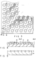
- FIG. 3 is a plan view, showing a conventional TAB tape of a three-layer structure. FIG. 4 is a cross sectional view, showing the TAB tape of FIG. 3. The TAB tape shown in FIGS. 3 and 4 comprises a
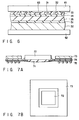
resin tape 35 made of polyimide, an adhesive 34 coated on the resin tape, andcopper foil patterns copper foil patterns copper foil patterns adhesive 34 are coated with solder resist 33 which protects them. A hole is formed in the portion of thesolder resist 33 which is located on each pad 31a. Supposing that each copper foil pattern has a film thickness of 18 µm, the difference in level is also 18 µm between the upper surface of each of the portions of thesolder resist 35 which are coated on thecopper foil patterns adhesive 34. - FIG. 5 shows a stiffener, to which the
polyimide tape 35 of the TAB tape is adhered. This stiffener is for a BGA tape, and comprises ametal plate 52 and an adhesive 51 coated thereon. - FIG. 6 is a view, useful in explaining a process for adhering the TAB tape shown in FIG. 4 to the stiffener shown in FIG. 5 by thermo-compression bonding. In FIG. 6, elements similar to those shown in FIGS. 4 and 5 are denoted by corresponding reference numerals, and no explanation is given thereof. As is shown in FIG. 6, the TAB tape and the stiffener are held between
tools tools adhesive 51. - Thereafter, as shown in FIG. 7A, the
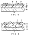
resultant TAB tape 74 is adhered to asemiconductor chip 72, thechip 72 is sealed with apotting resin 71, andsolder balls 75 are attached to the pads of theTAB tape 74, thereby forming a semiconductor device. FIG. 7B is a plan view of the semiconductor device shown in FIG. 7A. - In the FIG. 6 process for adhering the TAB tape to the stiffener by thermo-compression, the solder resist 33 has great irregularities as described above, and therefore the pressure from the upper and
lower tools concave portions 63 of the solder resist. Accordingly, theadhesive 51 are not sufficiently pressed at locations below theconcave portions 63, and hence may well have an insufficiently adheredportion 81 as shown in FIG 8. - Thereafter, when the
adhesive 51 is heated in a cure or reflow process, a babble will occur at the insufficiently adhered portion. FIG. 9 is a sectional view, showing the state of the BGA tape in which ababble 91 occurs therein. As is understood from FIG. 9, the BGA tape is warped due to thebabble 91, thereby degrading the flatness of a package, and it is difficult to make the lights the solder balls equal. - It is the object of the invention to securely adhere the TAB tape to the overall surface of a stiffener, thereby enhancing the flatness of package.
- To attain the object, the invention comprises a resin tape, pads formed on the resin tape, copper foil patterns constituting leads, dummy copper foil patterns provided between the copper foil patterns, and solder resist coated on the overall surfaces of the copper foil patterns and the dummy copper foil patterns.
- The invention can be more fully understood from the following detailed description when taken in conjunction with the accompanying drawings, in which:
- FIG. 1 is a sectional view, showing the embodiment of the invention;
- FIG. 2 is a plan view of the embodiment of FIG. 1;
- FIG. 3 is a plan view, showing a conventional TAB tape;
- FIG. 4 is a sectional view of the TAB tape shown in FIG. 3;
- FIG. 5 is a view, showing a stiffener for use in a BGA tape;
- FIG. 6 is a view, useful in explaining a process for adhering a TAB tape to a stiffener by thermo-compression;
- FIG. 7A is a sectional view, showing a semiconductor device;
- FIG. 7B is a plan view of the semiconductor device shown in FIG. 7A;
- FIG. 8 is a sectional view, showing a conventional BGA tape obtained after a thermo-compression adhesion treatment; and
- FIG. 9 is a sectional view, showing a conventional BGA tape obtained after a heat treatment.
- The embodiment of the invention will be described with reference to the accompanying drawings.
- FIG. 1 is a sectional view, showing a BGA tape according to the embodiment of the invention. FIG. 2 is a plan view of the embodiment of FIG. 1. The sectional view of FIG. 1 is taken along lines I - I of FIG. 2.
- In the BGA tape of the embodiment, an adhesive 14 is coated on one surface of a
resin tape 15 made, for example, of polyimide. Metallic patterns, for example,copper foil patterns 19 are formed on the adhesive 14. Thecopper foil patterns 19 consists ofpads 11 to which solder balls are attached, and leads 12 for connecting thepads 11 to a semiconductor chip. Eachlead 12 has a width of e.g. 30 - 60 µm. - The
adhesive 14 is provided with dummymetallic patterns 10, 10a, 10b such ascopper foil patterns 19. The dummy metallic pattern means a pattern electrically connected between thepad 11 and thelead 12, and having a width greater than thelead 12, or a pattern electrically connected neither to thepad 11 nor to thelead 12. The width of the pattern is, for example, 600 - 800 µm at maximum. - The copper foil patterns 10 - 12 are coated with solder resist 13. The opposite side of the
polyimide tape 15 is adhered to ametal plate 17 by means of an adhesive 16. Themetal plate 17 and theadhesive 16 are constitute a stiffener. - As is shown in FIGS. 1 and 2, each of
dummy patterns 10, 10a, 10b is formed in a wide space defined between adjacent ones of thepads 11 or of theleads 12, or between eachpad 11 and acorresponding lead 12. In general, thedummy patterns 10 are formed simultaneous with thepads 11 and thelead 12. The dummy pattern may be formed independent of the other elements asdummy patterns 10, 10a, or connected to thepad 11 as a dummy pattern 10b, or grounded. - In the embodiment, the areas of the portions of the
adhesive 14 which are exposed in a stage before the coating of the solder resist 13 are minimized by providing thedummy patterns 10, 10a, 10b on the adhesive 14. Since the solder resist 13 is applied in this stage, the difference in level is minimized between the upper surface of each of the portions of the solder resist 13 which are coated on thecopper foil patterns 19, and the upper surface of each of the portions of the solder resist 13 which are coated on the exposed portions of the adhesive 14. If the film thickness of thecopper foil patterns 19 is 18 µm, the difference in level can be reduced to 3 - 18 µm, more particularly to 7 µm or less. - Accordingly, at the time of adhering the stiffener to the TAB tape, a uniform pressure can be applied to the overall adhesive, with the result that no insufficiently adhered portions will be formed between the adhesive 16 and the
TAB tape 15, and hence no babbles will occur therebetween. Thus, the adhesion between the adhesive 16 and theTAB tape 15 will be enhanced. - Moreover, since the contact area between the adhesive 14 and the copper foil patterns is increased by connecting dummy patterns to leads and pads, the strength of adhesion between the
TAB tape 15 and the copper foil is increased. - In addition, grounding the dummy patterns formed between the pads will reduce the inductance between each pair of adjacent pads.
- Although in the above-described embodiment, the TAB tape has a three-layer structure, the invention is not limited to this. The TAB tape may have a double layer structure consisting of a resin tape and a copper foil pattern layer. Also, the patterns and the dummy patterns are not limited to copper foil patterns.
Claims (10)
- A semiconductor device characterized by comprising:a resin tape (15);metallic patterns (19) including pads (11) and leads (12) formed on the resin tape;solder resist (13) coated on the metallic patterns and on exposed portions of the resin tape between the metallic patterns; anddummy metallic patterns (10, 10a, 10b) provided between the metallic patterns (19) and coated with the solder resist, thereby reducing differences in level between upper surfaces of the metallic patterns.
- The semiconductor device according to claim 1, characterized in that each of the dummy metallic patterns (10) is formed of one of a pattern having a width greater than each of the leads, and a pattern connected neither to the pads nor to the leads.
- The semiconductor device according to claim 1, characterized in that the sum of the thickness of each metallic pattern (19) and the thickness of the portion of the solder resist (13) which is provided on said each metallic pattern is greater, by an amount of from 3 µm to less than 8 µm, than the sum of the thickness of each dummy metallic pattern between corresponding adjacent ones of the metallic patterns and the thickness of the portion of the solder resist which is provided on said each dummy pattern.
- The semiconductor device according to claim 1, characterized in that each dummy metallic pattern (10b) is connected to a corresponding one of the pads (11) and a corresponding one of the leads (12).
- The semiconductor device according to claim 1, characterized in that the dummy metallic patterns (10) are grounded.
- The semiconductor device according to claim 1, characterized in that an adhesive (14) is coated between the resin tape (15) and the metallic patterns (19) and between the resin tape (15) and the dummy metallic patterns (10, 10a, 10b).
- The semiconductor device according to claim 1, characterized by further comprising a stiffener (17) adhered to a batch surface of the resin tape,
wherein said dummy metallic patterns enabling a uniform pressure to be applied to the stiffener at the time of adhering the resin tape to the stiffener with pressure. - The semiconductor device according to claim 7, characterized in that an adhesive (14) is coated between the resin tape (15) and the metallic patterns (19) and between the resin tape and the dummy metallic patterns (10).
- The semiconductor device according to claim 1, characterized in that said raisin tape (15), metaric patterns (19) and dummy metaric patterns (10, 10a, 10b) constitute a TAB tape.
- The TAB tape according to claim 9, characterized in that an adhesive (14) is coated between the resin tape (15) and the metallic patterns (19) and between the resin tape and the dummy metallic patterns (10).
Applications Claiming Priority (2)
| Application Number | Priority Date | Filing Date | Title |
|---|---|---|---|
| JP159686/96 | 1996-06-20 | ||
| JP15968696A JP3346985B2 (en) | 1996-06-20 | 1996-06-20 | Semiconductor device |
Publications (3)
| Publication Number | Publication Date |
|---|---|
| EP0814510A2 true EP0814510A2 (en) | 1997-12-29 |
| EP0814510A3 EP0814510A3 (en) | 1999-04-21 |
| EP0814510B1 EP0814510B1 (en) | 2006-06-21 |
Family
ID=15699111
Family Applications (1)
| Application Number | Title | Priority Date | Filing Date |
|---|---|---|---|
| EP97110042A Expired - Lifetime EP0814510B1 (en) | 1996-06-20 | 1997-06-19 | TAB tape and semiconductor device using the TAB tape |
Country Status (7)
| Country | Link |
|---|---|
| US (1) | US5892277A (en) |
| EP (1) | EP0814510B1 (en) |
| JP (1) | JP3346985B2 (en) |
| KR (1) | KR100253872B1 (en) |
| CN (1) | CN1087102C (en) |
| DE (1) | DE69736157T2 (en) |
| TW (1) | TW460996B (en) |
Cited By (2)
| Publication number | Priority date | Publication date | Assignee | Title |
|---|---|---|---|---|
| US6528417B1 (en) * | 2001-09-17 | 2003-03-04 | Taiwan Semiconductor Manufacturing Company | Metal patterned structure for SiN surface adhesion enhancement |
| US6909053B2 (en) * | 2001-10-02 | 2005-06-21 | Nec Lcd Technologies, Ltd. | Circuit substrate connecting structure, liquid crystal display device having the connecting structure and mounting method of liquid crystal display device |
Families Citing this family (15)
| Publication number | Priority date | Publication date | Assignee | Title |
|---|---|---|---|---|
| JP3638778B2 (en) * | 1997-03-31 | 2005-04-13 | 株式会社ルネサステクノロジ | Semiconductor integrated circuit device and manufacturing method thereof |
| US6194313B1 (en) * | 1997-04-30 | 2001-02-27 | Texas Instruments Incorporated | Method for reducing recess for the formation of local interconnect and or plug trench fill for etchback process |
| JP4307664B2 (en) * | 1999-12-03 | 2009-08-05 | 株式会社ルネサステクノロジ | Semiconductor device |
| TW469552B (en) * | 1999-12-10 | 2001-12-21 | Toshiba Corp | TAB type semiconductor device |
| US6501170B1 (en) | 2000-06-09 | 2002-12-31 | Micron Technology, Inc. | Substrates and assemblies including pre-applied adhesion promoter |
| US6555910B1 (en) * | 2000-08-29 | 2003-04-29 | Agere Systems Inc. | Use of small openings in large topography features to improve dielectric thickness control and a method of manufacture thereof |
| KR100378185B1 (en) * | 2000-10-16 | 2003-03-29 | 삼성전자주식회사 | Micro ball grid array package tape including tap for testing |
| JP4626919B2 (en) * | 2001-03-27 | 2011-02-09 | ルネサスエレクトロニクス株式会社 | Semiconductor device |
| WO2007093966A1 (en) * | 2006-02-15 | 2007-08-23 | Nxp B.V. | Non-conductive planarization of substrate surface for mold cap |
| TWI474458B (en) * | 2012-03-23 | 2015-02-21 | Chipmos Technologies Inc | Chip packaging substrate |
| US9275967B2 (en) * | 2014-01-06 | 2016-03-01 | Taiwan Semiconductor Manufacturing Company, Ltd. | Protrusion bump pads for bond-on-trace processing |
| US9418928B2 (en) | 2014-01-06 | 2016-08-16 | Taiwan Semiconductor Manufacturing Company, Ltd. | Protrusion bump pads for bond-on-trace processing |
| US9508637B2 (en) | 2014-01-06 | 2016-11-29 | Taiwan Semiconductor Manufacturing Company, Ltd. | Protrusion bump pads for bond-on-trace processing |
| US9305890B2 (en) | 2014-01-15 | 2016-04-05 | Taiwan Semiconductor Manufacturing Company, Ltd. | Package having substrate with embedded metal trace overlapped by landing pad |
| KR102214512B1 (en) * | 2014-07-04 | 2021-02-09 | 삼성전자 주식회사 | Printed circuit board and semiconductor package using the same |
Citations (5)
| Publication number | Priority date | Publication date | Assignee | Title |
|---|---|---|---|---|
| US4916514A (en) * | 1988-05-31 | 1990-04-10 | Unisys Corporation | Integrated circuit employing dummy conductors for planarity |
| US5162896A (en) * | 1987-06-02 | 1992-11-10 | Kabushiki Kaisha Toshiba | IC package for high-speed semiconductor integrated circuit device |
| EP0528323A1 (en) * | 1991-08-16 | 1993-02-24 | Motorola, Inc. | A tape automated bonding (TAB) semiconductor device and method for making the same |
| US5334858A (en) * | 1991-01-22 | 1994-08-02 | Kabushiki Kaisha Toshiba | Semiconductor device of tab structure, capable of ensuring ease of testing of same in final form |
| US5441915A (en) * | 1992-09-01 | 1995-08-15 | Taiwan Semiconductor Manufacturing Company Ltd. | Process of fabrication planarized metallurgy structure for a semiconductor device |
Family Cites Families (3)
| Publication number | Priority date | Publication date | Assignee | Title |
|---|---|---|---|---|
| JP2864705B2 (en) * | 1990-09-21 | 1999-03-08 | セイコーエプソン株式会社 | TAB film carrier tape and method for solder coating on its lead |
| JP3197291B2 (en) * | 1991-04-30 | 2001-08-13 | 株式会社リコー | TAB package |
| JPH088295A (en) * | 1994-06-20 | 1996-01-12 | Toshiba Corp | Semiconductor mounting device and its production |
-
1996
- 1996-06-20 JP JP15968696A patent/JP3346985B2/en not_active Expired - Fee Related
-
1997
- 1997-06-12 TW TW086108122A patent/TW460996B/en not_active IP Right Cessation
- 1997-06-19 US US08/879,304 patent/US5892277A/en not_active Expired - Fee Related
- 1997-06-19 EP EP97110042A patent/EP0814510B1/en not_active Expired - Lifetime
- 1997-06-19 DE DE69736157T patent/DE69736157T2/en not_active Expired - Lifetime
- 1997-06-20 CN CN97113834A patent/CN1087102C/en not_active Expired - Fee Related
- 1997-06-20 KR KR1019970026004A patent/KR100253872B1/en not_active IP Right Cessation
Patent Citations (5)
| Publication number | Priority date | Publication date | Assignee | Title |
|---|---|---|---|---|
| US5162896A (en) * | 1987-06-02 | 1992-11-10 | Kabushiki Kaisha Toshiba | IC package for high-speed semiconductor integrated circuit device |
| US4916514A (en) * | 1988-05-31 | 1990-04-10 | Unisys Corporation | Integrated circuit employing dummy conductors for planarity |
| US5334858A (en) * | 1991-01-22 | 1994-08-02 | Kabushiki Kaisha Toshiba | Semiconductor device of tab structure, capable of ensuring ease of testing of same in final form |
| EP0528323A1 (en) * | 1991-08-16 | 1993-02-24 | Motorola, Inc. | A tape automated bonding (TAB) semiconductor device and method for making the same |
| US5441915A (en) * | 1992-09-01 | 1995-08-15 | Taiwan Semiconductor Manufacturing Company Ltd. | Process of fabrication planarized metallurgy structure for a semiconductor device |
Non-Patent Citations (3)
| Title |
|---|
| PATENT ABSTRACTS OF JAPAN vol. 016, no. 397 (E-1252), 24 August 1992 & JP 04 130743 A (SEIKO EPSON CORP), 1 May 1992 * |
| PATENT ABSTRACTS OF JAPAN vol. 017, no. 174 (E-1346), 5 April 1993 & JP 04 329649 A (RICOH CO LTD), 18 November 1992 * |
| PATENT ABSTRACTS OF JAPAN vol. 096, no. 005, 31 May 1996 & JP 08 008295 A (TOSHIBA CORP), 12 January 1996 * |
Cited By (2)
| Publication number | Priority date | Publication date | Assignee | Title |
|---|---|---|---|---|
| US6528417B1 (en) * | 2001-09-17 | 2003-03-04 | Taiwan Semiconductor Manufacturing Company | Metal patterned structure for SiN surface adhesion enhancement |
| US6909053B2 (en) * | 2001-10-02 | 2005-06-21 | Nec Lcd Technologies, Ltd. | Circuit substrate connecting structure, liquid crystal display device having the connecting structure and mounting method of liquid crystal display device |
Also Published As
| Publication number | Publication date |
|---|---|
| JP3346985B2 (en) | 2002-11-18 |
| DE69736157D1 (en) | 2006-08-03 |
| CN1170234A (en) | 1998-01-14 |
| CN1087102C (en) | 2002-07-03 |
| KR100253872B1 (en) | 2000-04-15 |
| EP0814510B1 (en) | 2006-06-21 |
| US5892277A (en) | 1999-04-06 |
| KR980005944A (en) | 1998-03-30 |
| JPH1012676A (en) | 1998-01-16 |
| TW460996B (en) | 2001-10-21 |
| DE69736157T2 (en) | 2007-05-03 |
| EP0814510A3 (en) | 1999-04-21 |
Similar Documents
| Publication | Publication Date | Title |
|---|---|---|
| EP0814510A2 (en) | TAB tape and semiconductor device using the TAB tape | |
| US5329423A (en) | Compressive bump-and-socket interconnection scheme for integrated circuits | |
| KR100537972B1 (en) | Chip scale ball grid array for integrated circuit package | |
| US5367435A (en) | Electronic package structure and method of making same | |
| EP0948814B1 (en) | Chip scale ball grid array for integrated circuit package | |
| US6985362B2 (en) | Printed circuit board and electronic package using same | |
| EP0907204A2 (en) | Chip size package semiconductor device and method of forming the same | |
| EP0704896A2 (en) | Tape automated bonding type semiconductor device | |
| KR20010072583A (en) | Laminated integrated circuit package | |
| JPH0394459A (en) | Semiconductor chip module and manufacture thereof | |
| US5731636A (en) | Semiconductor bonding package | |
| JP2000332055A (en) | Flip-chip mounting structure and mounting method | |
| JP3871634B2 (en) | COF semiconductor device manufacturing method | |
| JP2753696B2 (en) | Automatic bonding structure of semiconductor package tape | |
| US20020096750A1 (en) | Package for semiconductor chip having thin recess portion and thick plane portion | |
| US6192579B1 (en) | Tape carrier and manufacturing method therefor | |
| JP2000077569A (en) | Board, semiconductor device and its manufacture | |
| US6818542B2 (en) | Tape circuit board and semiconductor chip package including the same | |
| US6281437B1 (en) | Method of forming an electrical connection between a conductive member having a dual thickness substrate and a conductor and electronic package including said connection | |
| US6504239B1 (en) | Semiconductor device having dummy pattern that relieves stress | |
| TWI228785B (en) | Substrate, wiring board, substrate for semiconductor package, semiconductor device, semiconductor package and its manufacturing method | |
| JP2000022329A (en) | Wiring board and electronic unit, and method of mounting electronic parts | |
| JPH0236556A (en) | Pin grid array and mounting of semiconductor element | |
| JPH0786340A (en) | Connection of semiconductor element | |
| JPH10233417A (en) | Semiconductor device and its manufacture |
Legal Events
| Date | Code | Title | Description |
|---|---|---|---|
| PUAI | Public reference made under article 153(3) epc to a published international application that has entered the european phase |
Free format text: ORIGINAL CODE: 0009012 |
|
| 17P | Request for examination filed |
Effective date: 19970710 |
|
| AK | Designated contracting states |
Kind code of ref document: A2 Designated state(s): DE FR GB |
|
| PUAL | Search report despatched |
Free format text: ORIGINAL CODE: 0009013 |
|
| AK | Designated contracting states |
Kind code of ref document: A3 Designated state(s): AT BE CH DE DK ES FI FR GB GR IE IT LI LU MC NL PT SE |
|
| AKX | Designation fees paid |
Free format text: DE FR GB |
|
| 17Q | First examination report despatched |
Effective date: 20030808 |
|
| GRAP | Despatch of communication of intention to grant a patent |
Free format text: ORIGINAL CODE: EPIDOSNIGR1 |
|
| GRAS | Grant fee paid |
Free format text: ORIGINAL CODE: EPIDOSNIGR3 |
|
| GRAA | (expected) grant |
Free format text: ORIGINAL CODE: 0009210 |
|
| AK | Designated contracting states |
Kind code of ref document: B1 Designated state(s): DE FR GB |
|
| REG | Reference to a national code |
Ref country code: GB Ref legal event code: FG4D |
|
| REF | Corresponds to: |
Ref document number: 69736157 Country of ref document: DE Date of ref document: 20060803 Kind code of ref document: P |
|
| ET | Fr: translation filed | ||
| PLBE | No opposition filed within time limit |
Free format text: ORIGINAL CODE: 0009261 |
|
| STAA | Information on the status of an ep patent application or granted ep patent |
Free format text: STATUS: NO OPPOSITION FILED WITHIN TIME LIMIT |
|
| 26N | No opposition filed |
Effective date: 20070322 |
|
| PGFP | Annual fee paid to national office [announced via postgrant information from national office to epo] |
Ref country code: FR Payment date: 20100709 Year of fee payment: 14 |
|
| PGFP | Annual fee paid to national office [announced via postgrant information from national office to epo] |
Ref country code: GB Payment date: 20100616 Year of fee payment: 14 Ref country code: DE Payment date: 20100616 Year of fee payment: 14 |
|
| GBPC | Gb: european patent ceased through non-payment of renewal fee |
Effective date: 20110619 |
|
| REG | Reference to a national code |
Ref country code: FR Ref legal event code: ST Effective date: 20120229 |
|
| REG | Reference to a national code |
Ref country code: DE Ref legal event code: R119 Ref document number: 69736157 Country of ref document: DE Effective date: 20120103 |
|
| PG25 | Lapsed in a contracting state [announced via postgrant information from national office to epo] |
Ref country code: DE Free format text: LAPSE BECAUSE OF NON-PAYMENT OF DUE FEES Effective date: 20120103 Ref country code: FR Free format text: LAPSE BECAUSE OF NON-PAYMENT OF DUE FEES Effective date: 20110630 |
|
| PG25 | Lapsed in a contracting state [announced via postgrant information from national office to epo] |
Ref country code: GB Free format text: LAPSE BECAUSE OF NON-PAYMENT OF DUE FEES Effective date: 20110619 |