EP0814416B1 - Match and match address signal generation in a content addressable memory encoder - Google Patents
Match and match address signal generation in a content addressable memory encoder Download PDFInfo
- Publication number
- EP0814416B1 EP0814416B1 EP97303966A EP97303966A EP0814416B1 EP 0814416 B1 EP0814416 B1 EP 0814416B1 EP 97303966 A EP97303966 A EP 97303966A EP 97303966 A EP97303966 A EP 97303966A EP 0814416 B1 EP0814416 B1 EP 0814416B1
- Authority
- EP
- European Patent Office
- Prior art keywords
- match
- signal
- bit
- cam
- address
- Prior art date
- Legal status (The legal status is an assumption and is not a legal conclusion. Google has not performed a legal analysis and makes no representation as to the accuracy of the status listed.)
- Expired - Lifetime
Links
Images

Classifications
-
- H—ELECTRICITY
- H03—ELECTRONIC CIRCUITRY
- H03M—CODING; DECODING; CODE CONVERSION IN GENERAL
- H03M7/00—Conversion of a code where information is represented by a given sequence or number of digits to a code where the same, similar or subset of information is represented by a different sequence or number of digits
- H03M7/30—Compression; Expansion; Suppression of unnecessary data, e.g. redundancy reduction
- H03M7/3084—Compression; Expansion; Suppression of unnecessary data, e.g. redundancy reduction using adaptive string matching, e.g. the Lempel-Ziv method
-
- G—PHYSICS
- G06—COMPUTING OR CALCULATING; COUNTING
- G06F—ELECTRIC DIGITAL DATA PROCESSING
- G06F16/00—Information retrieval; Database structures therefor; File system structures therefor
- G06F16/90—Details of database functions independent of the retrieved data types
- G06F16/903—Querying
- G06F16/90335—Query processing
- G06F16/90339—Query processing by using parallel associative memories or content-addressable memories
-
- G—PHYSICS
- G11—INFORMATION STORAGE
- G11C—STATIC STORES
- G11C15/00—Digital stores in which information comprising one or more characteristic parts is written into the store and in which information is read-out by searching for one or more of these characteristic parts, i.e. associative or content-addressed stores
- G11C15/04—Digital stores in which information comprising one or more characteristic parts is written into the store and in which information is read-out by searching for one or more of these characteristic parts, i.e. associative or content-addressed stores using semiconductor elements
Definitions
- the present invention relates generally to the encoding of digital data and, more specifically, to MATCH and MATCH_ADDRESS signal generation in a content addressable memory encoder.
- Random access memory is perhaps the most common form of integrated circuit memory available in the state of the art.
- RAM devices are not suited for use in systems which process associative data.
- the well known methodology of sequentially accessing data when addressing the RAM is inefficient for systems involving stored information involving pattern recognition, natural language recognition, sparse matrix processes, and data-base interrogation.
- the address associated with the desired stored data may not be known.
- it is more efficient to interrogate a memory by supplying a compressed subset of the desired data or a code representative of the full data set.
- the memory responds by indicating either absence of the desired data set by a MISMATCH signal, or presence of the data set by a MATCH signal, and its associated address in the memory bank for the data set.
- CAM content addressable memory
- a string dictionary can be stored in a CAM and used in generating Lev-Zempel compressed output data (hereinafter "LZ"; generically used for any LZ data compression technique; see “Compression of Individual Sequences Via Variable-Rate Coding", IEEE Transactions on Information Theory, 24(5):530-536, September 1978).
- LZ Lev-Z
- the input data signal to the CAM would comprise a bit string representation of the data which is being searched for in the CAM.
- the output would be a signal indicative as to whether the data was found, the MATCH signal, and, if found, the location within the CAM, the MATCH ADDRESS.
- a data base may be stored in a CAM where the data consists of bit strings comprising tristimulus space values - cyan, yellow, magenta ("CYM").
- CAM devices compared to RAM each individual cell structure is relatively complex. See e.g. , U.S. Pat. No. 4,780,845 (Threewitt). Thus, for the same integrated circuit real estate, a CAM device can not match the density, speed, or low-power performance of a RAM device. Integrated circuit process improvements generally affect both types of devices equally, so that in relative terms, CAM architects can not do much to narrow the performance gap.
- the search cycle that is, the time from receipt of an input data signal, or code, to the encoder input to determine if the CAM has the desired data set to the time of the output of a match or mismatch indication, and, if a MATCH signal is generated, the MATCH_ADDRESS.
- the present invention provides an encoder apparatus for a CAM, having a cell array of addressable cell means for storage of data bits therein and appropriate CAM output circuitry for transmitting selected data.
- the apparatus includes: a first encoding mechanism for receiving the CAM cell array output, the first encoding mechanism further including a MATCH signal line connected to each cell, a plurality of MATCH ADDRESS signal lines, and wherein the MATCH signal line and each of the MATCH ADDRESS signal lines have an identical number of substantially identical switching mechanism for indicating a change in digital state value on the MATCH signal and MATCH ADDRESS signal lines, respectively, wherein the MATCH signal line includes one of the switching mechanism for one-half of the cells in the cell array and wherein a predetermined one of the switching mechanism on the MATCH ADDRESS signal lines designates both a binary digit of the MATCH ADDRESS signal and a MATCH signal on lines for MATCH signals not having a MATCH signal line switching mechanism; and first output bus mechanism for transmitting MATCH signals and MATCH
- Embodiments of the apparatus and method are also explained for an implementation of an encoder apparatus for MATCH signal and MATCH ADDRESS signal generation for a bank of memory that includes a plurality of content addressable memory cores.
- implementations can be designed to reduce power consumption.
- SEARCH DATA on standard bus 101 is fed from the search engine (e.g., a central processing unit (not shown)) through a driver 103, comprising standard buffering hardware as would be known in the art to drive relatively the high capacitance of cam core cell architecture.
- the search engine e.g., a central processing unit (not shown)
- driver 103 comprising standard buffering hardware as would be known in the art to drive relatively the high capacitance of cam core cell architecture.
- the SEARCH_DATA is input through standard buses 107 1 - 107 N to interrogate each CAM_CORE 105 1 - 105 N . While for implementation for certain algorithms more than one CAM_CORE 105 1 - 105 N could have a MATCH, it is assumed in this exemplary embodiment implementation that only one cell on one CAM_CORE 105 1 - 105 N contains the data set of interest. Thus, if any, there will be only one MATCH x signal and one corresponding FIRST_MATCH_ADDRESS x .
- Each CAM_CORE 105 1 -105 N has an output bus 109 1 - 109 N with one line for each of the stored data words, viz. 128_words in the exemplary embodiment. If a mismatch occurs for any location, the output bit for that location is pulled to LOW to indicate a MISMATCH; thus, if an output stays HIGH, it indicates a MATCH.
- each CAM_CORE 105 1 - 105 n one hundred and twenty eight outputs on respective buses 109 1 - 109 N tell whether a particular address in that cell array is a MATCH or a MISMATCH.
- the output signal derivation for each CAM_CORE output of the six device memory bank is accomplished using a memory FIRST_ENCODER 111 1 - 111 N .
- the one hundred and twenty eight outputs of the six CAM_COREs 105 1 - 105 6 now need to be turned into a final match signal, MATCH_SIGNAL F , and DATA_MATCH_ADDRESS F signal, preferably in one clock cycle, where DATA_MATCH_ADDRESS F is both the address of a particular CAM_CORE 105 x and its cell array address, FIRST_MATCH_ADDRESS x .
- CAM_CORE 1 105 1 through CAM_CORE N 105 N a MATCHF signal and an appropriate DATA_MATCH_ADDRESS F is derived using FINAL_ENCODER 113.
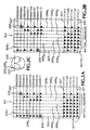
- FIG. 2A a standard CAM encoder 201, FIG. 2A, is shown.
- Such an encoder 201 is used in a CAM system such as shown in the assignee's U.S. Patent No. 5,373,290 (Lempel et al.) as element 194, FIG. 5, explained beginning in column 12, line 28 et seq.
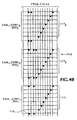
- a MATCH line 203 has a pull down transistor 205, configured as in FIGURE 2C, one for each of the one hundred and twenty eight data words in each CAM CORE 105 1 - 105 N .
- one hundred and twenty eight CORE_MATCH lines 207 0000000 (location zero) through 207 1111111 (location 127) are multiplexed to the MATCH line 203, from a least significant bit ("LSB") MATCH_ADDRESS line 209 1 through a most significant bit (“MSB) MATCH_ADDRESS line 209 7 , in essence a multiplex wired OR configuration [note: as will be described hereinafter, seven bits will also form the lower address bits of a ten bit address from the FINAL_ENCODER 113, FIG. 1].
- the MATCH line 203 has one hundred and twenty eight pull down transistors 205 (counted vertically in FIG. 2A), but each of the MATCH_ADDRESS lines 209 1 - 209 7 has only sixty four pull down transistors.
- every other MATCH line 203 has a pull down transistor 205
- the DATA of interest of the SEARCH_DATA is at location 0000011
- a location having no MATCH line 203 pull down transistor 205 but using bit_0 to do the double duty since only one location of the CAM_CORE is ever a match, no conflicts will occur. That is, if the CAM CORE has set the MATCH ADDRESS at location 0000011, bit_0 has change state, indicating a MATCH.
- the most significant MATCH_ADDRESS bit is used for the double duty, only the top sixty-four MATCH lines 203 require pull down transistors 205.
- This function is accomplished in the FINAL_ENCODER 113 by adding three upper address bits to the seven FIRST_MATCH_ADDRESS bits for the CAM_CORE 105 location where the full data of interest resides
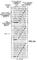
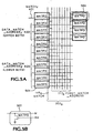
- FIGURES 3A - 3B and 4A - 4B a FINAL_ENCODER 113 for accomplishing this task is provided.
- FIGURE 3A again refers to an embodiment as shown in assignee's U.S. Patent No. 5,373,290 as part of element 194, FIG. 5.
- a final_encoder 301 for an array of six cam_cores has six sections, one designated for each cam_core of the array.
- each FIRST_ENCODER 111 1-N FIGURE 1, has an output line 115 1-N for a MATCH 1-N signal and an output bus 117 1-N for a FIRST_MATCH_ADDRESS 1-N .
- FIGURE 1 For CAM_CORE 6 as an example of each section, the MATCH 6 signal on line 115 6 provides an appropriate HIGH or LOW state signal to each respective FINAL_ENCODER 113 input subsection, CAM_CORE 1-N , 303 1-N .
- Each FIRST_MATCH_ADDRESS 7-bit bus 117 1-N is likewise input to each FINAL_ENCODER 113 input subsection, CAM_CORE 1-N .
- each CAM_CORE x has its respective FIRST_ENCODER 111 x output connected to a respective subsection of the FINAL_ENCODER 113 which will in turn provide the actual MATCH F signal and DATA_MATCH_ADDRESS F for the data of interest based on the SEARCH_DATA input.
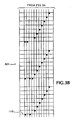
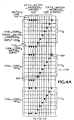
- FIGURES 5A and 5B detail for FINAL_ENCODER 113 subsection CAM_CORE 6 303 6 is depicted.
- the FINAL_ENCODER 113 is multiplexed with the inputs 115, 117 from the FIRST_ENCODER x .
- Match signal pull down transistors 501 are provided in a manner such that when a MATCH 6 and FIRST_MATCH_ADDRESS 6 is received from a FIRST_ENCODER 6 , the FINAL_ENCODER input subsection CAM_CORE 6 will provide both a MATCHF signal on FINAL_MATCH_LINE 401 and an expanded, 10-bit address for the data, DATA_MATCH_ADDRESS F .
- each CAM_CORE x can be compared and it can be seen that the removal of half of the pull down transistors 205 on FIRST_ENCODER_MATCH lines 207 in FIGURE 2B for providing the MATCH x signal has been added back in the FINAL_ENCODER 113 on MATCH F lines 401.
- this arrangement in the critical path in the present invention as shown in FIGURES 2B, 4A - 4B, and 5A - 5B provides an improvement of in reducing the cycle time approximate ten percent over the arrangement of FIGURES 2A, 3A - 3B in a synergistic manner.
Landscapes
- Engineering & Computer Science (AREA)
- Theoretical Computer Science (AREA)
- Databases & Information Systems (AREA)
- Computational Linguistics (AREA)
- Data Mining & Analysis (AREA)
- Physics & Mathematics (AREA)
- General Engineering & Computer Science (AREA)
- General Physics & Mathematics (AREA)
- Compression, Expansion, Code Conversion, And Decoders (AREA)
Applications Claiming Priority (2)
| Application Number | Priority Date | Filing Date | Title |
|---|---|---|---|
| US664902 | 1991-03-05 | ||
| US08/664,902 US5828324A (en) | 1996-06-17 | 1996-06-17 | Match and match address signal generation in a content addressable memory encoder |
Publications (3)
| Publication Number | Publication Date |
|---|---|
| EP0814416A2 EP0814416A2 (en) | 1997-12-29 |
| EP0814416A3 EP0814416A3 (en) | 1999-12-15 |
| EP0814416B1 true EP0814416B1 (en) | 2003-04-02 |
Family
ID=24667919
Family Applications (1)
| Application Number | Title | Priority Date | Filing Date |
|---|---|---|---|
| EP97303966A Expired - Lifetime EP0814416B1 (en) | 1996-06-17 | 1997-06-09 | Match and match address signal generation in a content addressable memory encoder |
Country Status (3)
| Country | Link |
|---|---|
| US (1) | US5828324A (enExample) |
| EP (1) | EP0814416B1 (enExample) |
| JP (1) | JPH10106274A (enExample) |
Families Citing this family (9)
| Publication number | Priority date | Publication date | Assignee | Title |
|---|---|---|---|---|
| JP3196720B2 (ja) * | 1998-03-20 | 2001-08-06 | 日本電気株式会社 | 連想メモリ制御回路及び制御方法 |
| US6892272B1 (en) | 1999-02-23 | 2005-05-10 | Netlogic Microsystems, Inc. | Method and apparatus for determining a longest prefix match in a content addressable memory device |
| US6191969B1 (en) * | 1999-09-09 | 2001-02-20 | Net Logic Microsystems, Inc. | Selective match line discharging in a partitioned content addressable memory array |
| US6392910B1 (en) * | 1999-09-10 | 2002-05-21 | Sibercore Technologies, Inc. | Priority encoder with multiple match function for content addressable memories and methods for implementing the same |
| US6934795B2 (en) | 1999-09-23 | 2005-08-23 | Netlogic Microsystems, Inc. | Content addressable memory with programmable word width and programmable priority |
| US6944709B2 (en) | 1999-09-23 | 2005-09-13 | Netlogic Microsystems, Inc. | Content addressable memory with block-programmable mask write mode, word width and priority |
| US7272027B2 (en) | 1999-09-23 | 2007-09-18 | Netlogic Microsystems, Inc. | Priority circuit for content addressable memory |
| US7143231B1 (en) | 1999-09-23 | 2006-11-28 | Netlogic Microsystems, Inc. | Method and apparatus for performing packet classification for policy-based packet routing |
| US6348881B1 (en) | 2000-08-29 | 2002-02-19 | Philips Electronics No. America Corp. | Efficient hardware implementation of a compression algorithm |
Family Cites Families (11)
| Publication number | Priority date | Publication date | Assignee | Title |
|---|---|---|---|---|
| US3701980A (en) * | 1970-08-03 | 1972-10-31 | Gen Electric | High density four-transistor mos content addressed memory |
| US4780845A (en) * | 1986-07-23 | 1988-10-25 | Advanced Micro Devices, Inc. | High density, dynamic, content-addressable memory cell |
| US4881075A (en) * | 1987-10-15 | 1989-11-14 | Digital Equipment Corporation | Method and apparatus for adaptive data compression |
| US4847619A (en) * | 1987-10-19 | 1989-07-11 | Hewlett-Packard Company | Performance-based reset of data compression dictionary |
| AU624205B2 (en) * | 1989-01-23 | 1992-06-04 | General Electric Capital Corporation | Variable length string matcher |
| US5373290A (en) * | 1991-09-25 | 1994-12-13 | Hewlett-Packard Corporation | Apparatus and method for managing multiple dictionaries in content addressable memory based data compression |
| US5175543A (en) * | 1991-09-25 | 1992-12-29 | Hewlett-Packard Company | Dictionary reset performance enhancement for data compression applications |
| US5555397A (en) * | 1992-01-10 | 1996-09-10 | Kawasaki Steel Corporation | Priority encoder applicable to large capacity content addressable memory |
| US5351208A (en) * | 1992-04-27 | 1994-09-27 | Integrated Information Technology, Inc. | Content addressable memory |
| US5455576A (en) * | 1992-12-23 | 1995-10-03 | Hewlett Packard Corporation | Apparatus and methods for Lempel Ziv data compression with improved management of multiple dictionaries in content addressable memory |
| JP3007819B2 (ja) * | 1994-12-28 | 2000-02-07 | インターナショナル・ビジネス・マシーンズ・コーポレイション | データ圧縮用検索装置 |
-
1996
- 1996-06-17 US US08/664,902 patent/US5828324A/en not_active Expired - Lifetime
-
1997
- 1997-06-09 EP EP97303966A patent/EP0814416B1/en not_active Expired - Lifetime
- 1997-06-17 JP JP9159409A patent/JPH10106274A/ja active Pending
Also Published As
| Publication number | Publication date |
|---|---|
| EP0814416A3 (en) | 1999-12-15 |
| EP0814416A2 (en) | 1997-12-29 |
| US5828324A (en) | 1998-10-27 |
| JPH10106274A (ja) | 1998-04-24 |
Similar Documents
| Publication | Publication Date | Title |
|---|---|---|
| US6069573A (en) | Match and match address signal prioritization in a content addressable memory encoder | |
| US5978885A (en) | Method and apparatus for self-timing associative data memory | |
| US7243290B2 (en) | Data encoding for fast CAM and TCAM access times | |
| EP0380294B1 (en) | String matching | |
| US6748405B2 (en) | Method and circuits for performing the quick search of the minimum/maximum value among a set of numbers | |
| US6108747A (en) | Method and apparatus for cyclically searching a contents addressable memory array | |
| US6243281B1 (en) | Method and apparatus for accessing a segment of CAM cells in an intra-row configurable CAM system | |
| US6845024B1 (en) | Result compare circuit and method for content addressable memory (CAM) device | |
| US6392910B1 (en) | Priority encoder with multiple match function for content addressable memories and methods for implementing the same | |
| USRE40932E1 (en) | Content addressable memory (CAM) devices that perform pipelined multi-cycle look-up operations using cam sub-arrays and longest match detection | |
| US6081442A (en) | Contents addressable memory circuit for retrieval operation in units of data blocks | |
| EP0634839A1 (en) | Data search device | |
| US5319762A (en) | Associative memory capable of matching a variable indicator in one string of characters with a portion of another string | |
| US5125098A (en) | Finite state-machine employing a content-addressable memory | |
| HK1009317B (en) | String matching | |
| WO1999059154A1 (en) | Method and apparatus for a serial access memory | |
| EP0814416B1 (en) | Match and match address signal generation in a content addressable memory encoder | |
| USRE42684E1 (en) | Word search in content addressable memory | |
| US6718433B1 (en) | Match and priority encoding logic circuit | |
| US6751701B1 (en) | Method and apparatus for detecting a multiple match in an intra-row configurable CAM system | |
| US6868475B2 (en) | Content addressable memory having data width extension capability | |
| JP3166838B2 (ja) | プライオリティ・エンコーダ及びプライオリティ・エンコード方法 | |
| US6799243B1 (en) | Method and apparatus for detecting a match in an intra-row configurable cam system | |
| GB2182789A (en) | A content addressable memory | |
| US6801981B1 (en) | Intra-row configurability of content addressable memory |
Legal Events
| Date | Code | Title | Description |
|---|---|---|---|
| PUAI | Public reference made under article 153(3) epc to a published international application that has entered the european phase |
Free format text: ORIGINAL CODE: 0009012 |
|
| AK | Designated contracting states |
Kind code of ref document: A2 Designated state(s): FR GB IT |
|
| PUAL | Search report despatched |
Free format text: ORIGINAL CODE: 0009013 |
|
| AK | Designated contracting states |
Kind code of ref document: A3 Designated state(s): AT BE CH DE DK ES FI FR GB GR IE IT LI LU MC NL PT SE |
|
| 17P | Request for examination filed |
Effective date: 20000516 |
|
| AKX | Designation fees paid |
Free format text: FR GB IT |
|
| REG | Reference to a national code |
Ref country code: DE Ref legal event code: 8566 |
|
| RAP1 | Party data changed (applicant data changed or rights of an application transferred) |
Owner name: HEWLETT-PACKARD COMPANY, A DELAWARE CORPORATION |
|
| GRAH | Despatch of communication of intention to grant a patent |
Free format text: ORIGINAL CODE: EPIDOS IGRA |
|
| GRAH | Despatch of communication of intention to grant a patent |
Free format text: ORIGINAL CODE: EPIDOS IGRA |
|
| GRAA | (expected) grant |
Free format text: ORIGINAL CODE: 0009210 |
|
| AK | Designated contracting states |
Designated state(s): FR GB IT |
|
| REG | Reference to a national code |
Ref country code: GB Ref legal event code: FG4D |
|
| ET | Fr: translation filed | ||
| PLBE | No opposition filed within time limit |
Free format text: ORIGINAL CODE: 0009261 |
|
| STAA | Information on the status of an ep patent application or granted ep patent |
Free format text: STATUS: NO OPPOSITION FILED WITHIN TIME LIMIT |
|
| 26N | No opposition filed |
Effective date: 20040105 |
|
| PGFP | Annual fee paid to national office [announced via postgrant information from national office to epo] |
Ref country code: IT Payment date: 20070626 Year of fee payment: 11 |
|
| PGFP | Annual fee paid to national office [announced via postgrant information from national office to epo] |
Ref country code: FR Payment date: 20070618 Year of fee payment: 11 |
|
| REG | Reference to a national code |
Ref country code: FR Ref legal event code: ST Effective date: 20090228 |
|
| PG25 | Lapsed in a contracting state [announced via postgrant information from national office to epo] |
Ref country code: IT Free format text: LAPSE BECAUSE OF NON-PAYMENT OF DUE FEES Effective date: 20080609 Ref country code: FR Free format text: LAPSE BECAUSE OF NON-PAYMENT OF DUE FEES Effective date: 20080630 |
|
| PGFP | Annual fee paid to national office [announced via postgrant information from national office to epo] |
Ref country code: GB Payment date: 20100401 Year of fee payment: 14 |
|
| GBPC | Gb: european patent ceased through non-payment of renewal fee |
Effective date: 20110609 |
|
| PG25 | Lapsed in a contracting state [announced via postgrant information from national office to epo] |
Ref country code: GB Free format text: LAPSE BECAUSE OF NON-PAYMENT OF DUE FEES Effective date: 20110609 |