EP0813152A2 - Memory protection mechanism - Google Patents
Memory protection mechanism Download PDFInfo
- Publication number
- EP0813152A2 EP0813152A2 EP97301381A EP97301381A EP0813152A2 EP 0813152 A2 EP0813152 A2 EP 0813152A2 EP 97301381 A EP97301381 A EP 97301381A EP 97301381 A EP97301381 A EP 97301381A EP 0813152 A2 EP0813152 A2 EP 0813152A2
- Authority
- EP
- European Patent Office
- Prior art keywords
- memory
- address
- register
- block
- chip
- Prior art date
- Legal status (The legal status is an assumption and is not a legal conclusion. Google has not performed a legal analysis and makes no representation as to the accuracy of the status listed.)
- Granted
Links
Images


Classifications
-
- G—PHYSICS
- G06—COMPUTING; CALCULATING OR COUNTING
- G06F—ELECTRIC DIGITAL DATA PROCESSING
- G06F12/00—Accessing, addressing or allocating within memory systems or architectures
- G06F12/14—Protection against unauthorised use of memory or access to memory
-
- G—PHYSICS
- G06—COMPUTING; CALCULATING OR COUNTING
- G06F—ELECTRIC DIGITAL DATA PROCESSING
- G06F12/00—Accessing, addressing or allocating within memory systems or architectures
- G06F12/02—Addressing or allocation; Relocation
- G06F12/0223—User address space allocation, e.g. contiguous or non contiguous base addressing
- G06F12/0292—User address space allocation, e.g. contiguous or non contiguous base addressing using tables or multilevel address translation means
-
- G—PHYSICS
- G06—COMPUTING; CALCULATING OR COUNTING
- G06F—ELECTRIC DIGITAL DATA PROCESSING
- G06F12/00—Accessing, addressing or allocating within memory systems or architectures
- G06F12/02—Addressing or allocation; Relocation
-
- G—PHYSICS
- G06—COMPUTING; CALCULATING OR COUNTING
- G06F—ELECTRIC DIGITAL DATA PROCESSING
- G06F12/00—Accessing, addressing or allocating within memory systems or architectures
- G06F12/14—Protection against unauthorised use of memory or access to memory
- G06F12/1458—Protection against unauthorised use of memory or access to memory by checking the subject access rights
- G06F12/1466—Key-lock mechanism
- G06F12/1475—Key-lock mechanism in a virtual system, e.g. with translation means
-
- G—PHYSICS
- G06—COMPUTING; CALCULATING OR COUNTING
- G06F—ELECTRIC DIGITAL DATA PROCESSING
- G06F12/00—Accessing, addressing or allocating within memory systems or architectures
- G06F12/16—Protection against loss of memory contents
Definitions
- the invention relates to integrated circuits, and specifically to memory protection mechanism for use in an integrated circuit having a reduced instruction set computer (RISC) central processing unit (CPU), which may be used in portable devices.
- RISC reduced instruction set computer
- CPU central processing unit
- Portable devices include electronic instruments such as personal information manager, cellular telephones, digital cameras, hand-held games, bar-code scanners, medical equipment, electronic instrumentation, and navigation systems, specifically global positioning satellite navigation systems.
- portable devices require integrated circuits which are low in cost, have low power requirements to insure long battery life, and have high standards of performance to insure that their output is accurate and usable. Additionally, the interface between the integrated circuit and the remainder ot the portable device must be of a plug-and-play design so that a single type of integrated circuit may be used with a number of portable devices. Part of such flexibility is that the designer of a portable device must be able to easily incorporate the IC into the device as an off-the-shelf component, which does not require any internal modification to be used in a variety of applications.
- RISC Reduced instruction set computers
- the RISC architecture enables an IC to have a significantly smaller die size, because the smaller instruction set of the RISC technology requires fewer transistors to implement, which leads to simpler designs which consequently take less time to complete and to debug. Additionally, smaller chips having shorter signal paths mean that each instruction cycle is of a shorter duration.
- the relative size of a RISC CPU is significantly smaller than a CISC CPU, for instance, the Intel 386 SL chip is approximately 170 mm 2 , while a RISC chip having similar computational abilities is slightly more than 5 mm 2 .
- RISC-based CPUs make the RISC architecture ideal for "system-on-chip” (SOC) applications, wherein the CPU and a number of other structures are located on a single chip.
- SOC system-on-chip
- a SOC architecture will generally include the RISC CPU and some type of local RAM and/or data cache.
- the chip may include internal and external bus controllers, various types of communication ports, an interrupt controller, and pulse width modulator, various configuration registers, various timer/counter structures, and some type of output controller, such as an LCD controller.
- Such a structure may be configured in a 32-bit architecture, with associated peripherals integrated onto the chip, which integration allows the designer of the portable device incorporating the chip to reduce the development cycle and accelerate the product introduction to market.
- the chip structure may have an external 16-bit data bus with an integrated, programmable bus controller capable of supporting 8 or 16-bit SRAM, DRAM, EPROM and/or memory devices, which do not require additional buffers in order to function with the integrated circuit.
- the chip may be operated at either 3.3 volts or 5 volts, which will require between 100 mW and 350 mW, respectively.
- the integrated circuit may include a memory interface which provides multiple programmable chip enables, allowing users to set wait states and memory width, 8 or 16-bits wide.
- the integrated circuit provides for address decoding and DRAM control logic, which allows an external bus master to perform data transfers without requiring external address decoding or external DRAM controllers. In the case where sequential accesses are being used, the integrated circuit automatically increments the initial memory address supplied by the external bus master, thereby speeding transfers.
- the specific invention of this application relates to the segmenting of memory addresses which provides for a larger addressable memory space than would otherwise be expected from the 26-bit external address bus of the integrated circuit
- Up to eight segments of memory may be defined, each of which may be programmed for start and stop addresses, access privileges, cacheability, memory word-length criteria, and memory bank assignment. Because multiple segments are associated with the chip enable, a single physical memory block may be divided into user and supervisor segments for both data and program memory. Such an arrangement provides additional memory segments over the conventional enable structure, and allow for separation of memory blocks without sacrificing other control capabilities.
- Fig. 1 is block diagram of the system on chip structure of the invention.
- Fig. 2 is a detailed block diagram/flow chart of a portion of the system on chip structure of Fig. 1.
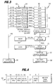
- Fig. 3 is a block diagram of the segmented memory structure of the invention.
- Fig. 4 is a block diagram of a segment descriptor register of the invention.
- IC 10 includes a RISC CPU 12 which is connected to a 32-bit internal bus 14.
- CPU 12 includes an embedded microcontroller 12 a therein in the preferred embodiment CPU 12 is directly connected to internal bus controller 16, which in turn is connected to bus 14 and to a bus, or memory, map 18.
- IC 10 further includes a local RAM (SRAM) 20, a combined instruction/data cache 22, and an external access port 24.
- SRAM local RAM
- IC 10 is intended to connect to a liquid crystal display (LCD) and to that end, includes a LCD controller 26 which is connected to an LCD panel interface 28.
- An external bus controller 30 is provided and is connected to an external memory interface 32 and external chip selects 34, which may be constructed as part of the external bus controller.
- a number of configuration registers 36 are provided, which may be constructed as a part of internal bus controller 16.
- a number of internal “peripherals” are connected to internal bus 14, and include a universal asynchronous receiver/transmitter (UART) 38, a parallel port 40, a timer/counter 42, an interrupt controller 44, and a pulse width modulator (PWM) 46.
- UART universal asynchronous receiver/transmitter
- PWM pulse width modulator
- IC 10 a portion of IC 10 is depicted.
- internal bus controller 16 includes a memory address register 48, a sequencer 50, and an arbitrator 52.
- the internal bus is depicted in two segments, 14 and 14 a .
- Memory address register 48 receives and stores a memory address from CPU 12 and attempts to locate that address in the various on-chip internal memory structures, such as cache 22, which is split into a cache Tag portion 22 a , and a cache data portion 22 b , local SRAM 20, memory map 18, or memory segments 54.
- the address is also passed to sequencer 50 and arbitrator 52 which determine whether the address is a sequential address from the previous memory address request (sequencer 50) and whether there are other operations that take priority over the present search on a particular clock cycle (arbitrator 52).
- sequencer 50 determines whether the address is a sequential address from the previous memory address request (sequencer 50) and whether there are other operations that take priority over the present search on a particular clock cycle (arbitrator 52).
- a signal is passed to memory map 18, which sends an abort signal 55 to the internal memory structures, with the exception of the structure that contains the next sequential address.
- external bus controller 30 will initiate a search for the address in external memory 56.
- Each segment includes three registers: A segment descriptor register (SDR) 60, a start register 62, and a stop register 64.
- SDR segment descriptor register
- a separate default SDR 66 is provided and is used after reset or, if-and-only-if (iff), in the event a search for the memory address is not found in SDRs 0 ⁇ -7.
- Memory segments 54 provide the addresses of multiple memory regions which are to be mapped to the same physical memory structures locations, either local RAM 20 or external memory 56. RAM 20 and external memory 56 both contain multiple memory regions located in a single physical location.
- a memory region, or memory bank may be defined in a physical memory structure by setting a starting memory address in one of the start registers 62 and by setting an ending memory address in one of the stop registers 64.
- Each SDR contains information about address characteristics, including system privileges, user privileges, cacheability, word length characteristics, and memory bank selection.
- Each segment may map to only one memory bank, represented generally by block 68, which is located in external memory 56.
- Start register 62 and stop register 64 determine the boundaries within memory of each segment
- Each start and stop register is a 32-bit register, and contains a start or stop address of 22-bits, in bit locations 10 ⁇ -31. Bits 0 ⁇ - 9 are zero-filled and are used to convert a 22-bit address to a 32-bit address.
- Default SDR 66 does not have start/stop registers associate therewith, as the default SDR spans the entire memory bank space. All of the start/stop registers will initialize to a zero-fill upon reset, forcing any external memory access to the default segment.
- Embedded microcontroller 12 a supports eight memory banks, six of which are for SRAM functions and two of which are for DRAM functions.
- a SRAM bank will reflect the properties of an external SRAM, such as chip selects, wait counts, and bus width.
- a DRAM bank will reflect the properties of an external DRAM such as nCAS (not Column Address Select), nRAS (not Row Address Select), memory bank size, page mode, wait count, and bus width.
- external bus controller 30 When external bus controller 30 receives an internal address for memory access from memory address register 48, it maps the address to the appropriate segment, or to the default segment, and performs all the necessary checks for privileges, block 70, and cacheability, block 72, according to the characteristics found in the appropriate SDR. Once all of the checks are passed external bus controller 30 accesses the appropriate memory bank 68, as indicated in the SDR.
- the memory bank signals external bus controller 30 which external device is to be selected and examines the properties of the external device. The lower 26 bits of the address are used to address the external device.
- Privileges are categorized as user read, user write, system read, and system write.
- SDR 60 is a 16-bit register which includes plural characteristic blocks, each of predetermined lengths.
- the blocks in SDR 60 are: in bits 0 ⁇ -7, memory bank selection indicators; in bit 8, word length mode indicator; in bit 10 ⁇ , cacheability indicator; in bits 11 and 12, user privilege indicators; and in bits 13 and 14, system privilege indicators.
- Memory bank selector block, bits 0 ⁇ -7, contains a binary 1 for bank 0 ⁇ , binary 2 for bank 1...and binary 8 for bank 7. These indicators are mutually exclusive, and any other entry is invalid.
- Word length mode indication may contain a 0 ⁇ or 1, indicating 32-bit mode or 16-bit mode, respectively.
- the cacheability indicator may contain a 0 ⁇ or 1, indicating that a segment is not cacheable or is cacheable, respectively. Privileges for system and users are indicated similarly: a logical 0 ⁇ indicates no privileges, logical (binary) 1 indicates read-only privileges, logical 2 indicates write only privileges and logical 3 indicates read/write privileges.
- Each segment may be individually programmed to give the user and/or the system read and/or write access to the memory space associated with the segment This allows for memory management and protection.
- both code and data may reside in the same external SRAM with the code accessible by the system only and the data by the system and the user. Any violation of the program privileges will cause an abort 74.
- Requests by LCD controller 26, in the preferred embodiment, are treated as system level requests and is accorded at least a system read privilege.
- a segment may be cacheable in which case any access to that segment will be handled by cache 22, or non-cacheable, in which case the access will be handled by external bus controller 30. Because the frame buffer for the LCD is located in main memory (off-chip) the segment containing the frame buffer may not be cached. The external bus controller will ignore the cacheability bit when it receives are request from the LCD controller.
- CPU 12 may be configured to support a variety of memory access requests, either in the form of a byte (8-bits) or a word (32-bits).
- embedded microcontroller 12 a has a 16-bit data bus, which requires a word access to take two clock cycles.
- a half-word mode enables the embedded micro controller to allow half-word accesses to external memory.
- the embedded microcontroller will treat all word accesses, whether read or write, and half-word accesses, the same, and will take one memory access, or clock cycle, to access the requested information.
- the 16-bit data from memory will be sign-extended in external bus controller 30 and sent to CPU 12 as a 32-bit word.
- external bus controller 30 will write the low order 16-bits of the word from CPU 12 to external memory 56. This protocol is particularly significant when IC 10 is connected to an off-chip device such as a flash memory.
- Bank select block includes eight mutually exclusive bits. A logical 1 in any bit position selects the memory bank associated with that position.
Abstract
Description
- The invention relates to integrated circuits, and specifically to memory protection mechanism for use in an integrated circuit having a reduced instruction set computer (RISC) central processing unit (CPU), which may be used in portable devices.
- Portable devices include electronic instruments such as personal information manager, cellular telephones, digital cameras, hand-held games, bar-code scanners, medical equipment, electronic instrumentation, and navigation systems, specifically global positioning satellite navigation systems.
- To be commercially successful, portable devices require integrated circuits which are low in cost, have low power requirements to insure long battery life, and have high standards of performance to insure that their output is accurate and usable. Additionally, the interface between the integrated circuit and the remainder ot the portable device must be of a plug-and-play design so that a single type of integrated circuit may be used with a number of portable devices. Part of such flexibility is that the designer of a portable device must be able to easily incorporate the IC into the device as an off-the-shelf component, which does not require any internal modification to be used in a variety of applications.
- The "computing power" found in integrated circuit CPUs, such as the Intel 80*86 and Pentium® series chips, and the Motorola 68000 series chips, has increased significantly over the last few years. At the same time, the size of such chips has grown significantly, as has their power requirements. Such chips are designated as conventional instruction set computers (CISC) and have come to require significant blocks of associated random access memory (RAM) while the applications that have been written to run on computers containing these chips have grown, seemingly without limit, requiring vast amounts of hard drive space. Such CISC devices are not easily usable with portable devices due to their power requirements and size.
- Reduced instruction set computers (RISC) were originally used in high-end graphics applications, and in CAE/CAD work stations. The RISC architecture, however, enables an IC to have a significantly smaller die size, because the smaller instruction set of the RISC technology requires fewer transistors to implement, which leads to simpler designs which consequently take less time to complete and to debug. Additionally, smaller chips having shorter signal paths mean that each instruction cycle is of a shorter duration. The relative size of a RISC CPU is significantly smaller than a CISC CPU, for instance, the Intel 386 SL chip is approximately 170 mm2, while a RISC chip having similar computational abilities is slightly more than 5 mm2.
- The small size of RISC-based CPUs makes the RISC architecture ideal for "system-on-chip" (SOC) applications, wherein the CPU and a number of other structures are located on a single chip. Such a SOC architecture may result in a chip that is still considerably smaller than a CISC CPU, but which contains all of the computational and control structures on a single integrated circuit. A SOC architecture will generally include the RISC CPU and some type of local RAM and/or data cache. Additionally, the chip may include internal and external bus controllers, various types of communication ports, an interrupt controller, and pulse width modulator, various configuration registers, various timer/counter structures, and some type of output controller, such as an LCD controller. Such a structure may be configured in a 32-bit architecture, with associated peripherals integrated onto the chip, which integration allows the designer of the portable device incorporating the chip to reduce the development cycle and accelerate the product introduction to market. The chip structure may have an external 16-bit data bus with an integrated, programmable bus controller capable of supporting 8 or 16-bit SRAM, DRAM, EPROM and/or memory devices, which do not require additional buffers in order to function with the integrated circuit. The chip may be operated at either 3.3 volts or 5 volts, which will require between 100 mW and 350 mW, respectively.
- By combining a number of peripherals on the chip, and providing an internal bus amongst the CPU and peripherals, it is possible to conduct a number of operations on chip, while simultaneously controlling off-chip operations, such as memory stores and retrieves.
- The integrated circuit may include a memory interface which provides multiple programmable chip enables, allowing users to set wait states and memory width, 8 or 16-bits wide. The integrated circuit provides for address decoding and DRAM control logic, which allows an external bus master to perform data transfers without requiring external address decoding or external DRAM controllers. In the case where sequential accesses are being used, the integrated circuit automatically increments the initial memory address supplied by the external bus master, thereby speeding transfers.
- The specific invention of this application relates to the segmenting of memory addresses which provides for a larger addressable memory space than would otherwise be expected from the 26-bit external address bus of the integrated circuit Up to eight segments of memory may be defined, each of which may be programmed for start and stop addresses, access privileges, cacheability, memory word-length criteria, and memory bank assignment. Because multiple segments are associated with the chip enable, a single physical memory block may be divided into user and supervisor segments for both data and program memory. Such an arrangement provides additional memory segments over the conventional enable structure, and allow for separation of memory blocks without sacrificing other control capabilities.
- These and other objects and advantages of the invention will become more fully apparent as the description which follows is read in connection with the drawings.
- Fig. 1 is block diagram of the system on chip structure of the invention.
- Fig. 2 is a detailed block diagram/flow chart of a portion of the system on chip structure of Fig. 1.
- Fig. 3 is a block diagram of the segmented memory structure of the invention.
- Fig. 4 is a block diagram of a segment descriptor register of the invention.
- Referring initially to Fig. 1, a system on chip (SOC) structure of the invention is depicted generally at 10. IC 10 includes a
RISC CPU 12 which is connected to a 32-bitinternal bus 14.CPU 12 includes an embeddedmicrocontroller 12a therein in thepreferred embodiment CPU 12 is directly connected tointernal bus controller 16, which in turn is connected tobus 14 and to a bus, or memory,map 18. IC 10 further includes a local RAM (SRAM) 20, a combined instruction/data cache 22, and anexternal access port 24. In the preferred embodiment, IC 10 is intended to connect to a liquid crystal display (LCD) and to that end, includes aLCD controller 26 which is connected to anLCD panel interface 28. Anexternal bus controller 30 is provided and is connected to anexternal memory interface 32 and external chip selects 34, which may be constructed as part of the external bus controller. - A number of
configuration registers 36 are provided, which may be constructed as a part ofinternal bus controller 16. A number of internal "peripherals" are connected tointernal bus 14, and include a universal asynchronous receiver/transmitter (UART) 38, aparallel port 40, a timer/counter 42, aninterrupt controller 44, and a pulse width modulator (PWM) 46. - Referring now to Fig. 2, a portion of
IC 10 is depicted. For purposes of this description,internal bus controller 16 is shown in more detail, and includes amemory address register 48, asequencer 50, and anarbitrator 52. The internal bus is depicted in two segments, 14 and 14a.Memory address register 48 receives and stores a memory address fromCPU 12 and attempts to locate that address in the various on-chip internal memory structures, such ascache 22, which is split into acache Tag portion 22a, and acache data portion 22b,local SRAM 20,memory map 18, ormemory segments 54. The address is also passed tosequencer 50 andarbitrator 52 which determine whether the address is a sequential address from the previous memory address request (sequencer 50) and whether there are other operations that take priority over the present search on a particular clock cycle (arbitrator 52). In the case where the memory address is sequential with the immediately prior request, a signal is passed tomemory map 18, which sends anabort signal 55 to the internal memory structures, with the exception of the structure that contains the next sequential address. In the event that the address is not found in any of the internal memory structures,external bus controller 30 will initiate a search for the address inexternal memory 56. - Referring now to Fig. 3,
plural memory segments 54 are depicted in greater detail, along with selected associated structures. In the preferred embodiment, there are eight memory segments, segments 0̸-7, shown generally at 58. Each segment includes three registers: A segment descriptor register (SDR) 60, astart register 62, and astop register 64. Aseparate default SDR 66 is provided and is used after reset or, if-and-only-if (iff), in the event a search for the memory address is not found in SDRs 0̸-7.Memory segments 54 provide the addresses of multiple memory regions which are to be mapped to the same physical memory structures locations, eitherlocal RAM 20 orexternal memory 56.RAM 20 andexternal memory 56 both contain multiple memory regions located in a single physical location. A memory region, or memory bank, may be defined in a physical memory structure by setting a starting memory address in one of thestart registers 62 and by setting an ending memory address in one of thestop registers 64. - Each SDR contains information about address characteristics, including system privileges, user privileges, cacheability, word length characteristics, and memory bank selection. Each segment may map to only one memory bank, represented generally by
block 68, which is located inexternal memory 56. Startregister 62 and stopregister 64 determine the boundaries within memory of each segment Each start and stop register is a 32-bit register, and contains a start or stop address of 22-bits, in bit locations 10̸-31. Bits 0̸ - 9 are zero-filled and are used to convert a 22-bit address to a 32-bit address.Default SDR 66 does not have start/stop registers associate therewith, as the default SDR spans the entire memory bank space. All of the start/stop registers will initialize to a zero-fill upon reset, forcing any external memory access to the default segment. - Embedded
microcontroller 12a supports eight memory banks, six of which are for SRAM functions and two of which are for DRAM functions. A SRAM bank will reflect the properties of an external SRAM, such as chip selects, wait counts, and bus width. A DRAM bank will reflect the properties of an external DRAM such as nCAS (not Column Address Select), nRAS (not Row Address Select), memory bank size, page mode, wait count, and bus width. - When
external bus controller 30 receives an internal address for memory access frommemory address register 48, it maps the address to the appropriate segment, or to the default segment, and performs all the necessary checks for privileges, block 70, and cacheability, block 72, according to the characteristics found in the appropriate SDR. Once all of the checks are passedexternal bus controller 30 accesses theappropriate memory bank 68, as indicated in the SDR. The memory bank signalsexternal bus controller 30 which external device is to be selected and examines the properties of the external device. The lower 26 bits of the address are used to address the external device. - By providing plural memory segments, the user may map two or more memory regions to the same physical external memory, so long as the memory region has different privileges, which will prevent the overwriting of selected privileged information. Privileges, as used herein, are categorized as user read, user write, system read, and system write.
- Referring now to Fig. 4,
representative SDR 60 is depicted.SDR 60 is a 16-bit register which includes plural characteristic blocks, each of predetermined lengths. The blocks inSDR 60 are: in bits 0̸-7, memory bank selection indicators; inbit 8, word length mode indicator; in bit 10̸, cacheability indicator; inbits bits binary 8 forbank 7. These indicators are mutually exclusive, and any other entry is invalid. Word length mode indication may contain a 0̸ or 1, indicating 32-bit mode or 16-bit mode, respectively. The cacheability indicator may contain a 0̸ or 1, indicating that a segment is not cacheable or is cacheable, respectively. Privileges for system and users are indicated similarly: a logical 0̸ indicates no privileges, logical (binary) 1 indicates read-only privileges, logical 2 indicates write only privileges and logical 3 indicates read/write privileges. - Each segment may be individually programmed to give the user and/or the system read and/or write access to the memory space associated with the segment This allows for memory management and protection. For example, both code and data may reside in the same external SRAM with the code accessible by the system only and the data by the system and the user. Any violation of the program privileges will cause an
abort 74. Requests byLCD controller 26, in the preferred embodiment, are treated as system level requests and is accorded at least a system read privilege. - A segment may be cacheable in which case any access to that segment will be handled by
cache 22, or non-cacheable, in which case the access will be handled byexternal bus controller 30. Because the frame buffer for the LCD is located in main memory (off-chip) the segment containing the frame buffer may not be cached. The external bus controller will ignore the cacheability bit when it receives are request from the LCD controller. -
CPU 12 may be configured to support a variety of memory access requests, either in the form of a byte (8-bits) or a word (32-bits). In one configuration ofCPU 12, embeddedmicrocontroller 12a has a 16-bit data bus, which requires a word access to take two clock cycles. A half-word mode enables the embedded micro controller to allow half-word accesses to external memory. The embedded microcontroller will treat all word accesses, whether read or write, and half-word accesses, the same, and will take one memory access, or clock cycle, to access the requested information. In the event of a word read, the 16-bit data from memory will be sign-extended inexternal bus controller 30 and sent toCPU 12 as a 32-bit word. In the event of a word write,external bus controller 30 will write the low order 16-bits of the word fromCPU 12 toexternal memory 56. This protocol is particularly significant whenIC 10 is connected to an off-chip device such as a flash memory. - Bank select block includes eight mutually exclusive bits. A logical 1 in any bit position selects the memory bank associated with that position.
- Because most address requests by
CPU 12 will be to internal locations, the need for additional clock cycles to locate off-chip addresses is greatly reduced by providingmemory segments 54. Particularly in the case where addresses are sequential, the memory contents will be retrieved within a single clock cycle. - Although a preferred embodiment of the memory protection mechanism of the invention has been disclosed herein, it should be appreciated that further variations and modifications may be made thereto without departing from the scope of the invention, as defined in the appended claims.
Claims (9)
- In an integrated circuit having a RISC CPU, a memory management module and on-chip internal memory structures, and connected to an off-chip, external memory structure, an on-chip memory protection mechanism for enhancing addressable memory space while prohibiting the overwriting of privileged memory contents, comprising:a memory map structure for mapping memory addresses of memory contents in the internal memory structures and in the external memory structure;address characteristic associated with each memory address,a memory address register for receiving and storing a memory address from the CPU; andplural memory segments for providing the addresses of multiple memory regions to be mapped to the sane physical memory structure location, wherein said multiple memory regions contain different memory contents having predetermined privileges, and for receiving information about said address characteristics, and wherein said plural memory segments, upon receipt of a memory address from said address register, compares the memory address to the multiple memory regions to locate the physical memory location.
- The memory protection mechanism of claim 1 wherein said plural memory segments each include a segment descriptor register for setting said address characteristics, a start register for receiving the starting address of a physical memory block, and a stop register for setting the ending address of a physical memory block
- The memory protection mechanism of claim 2 wherein said segment descriptor register includes plural characteristic blocks associated with the address characteristics, including a system privilege block, a user privileges block, a chacheability block, a word-length block, and a memory bank assignment block.
- The memory protection mechanism of claim 2 which includes a default segment descriptor register which is used after a system reset and iff a memory address does not match an address in any other segment descriptor register.
- In an integrated circuit having a RISC CPU, a memory management module and on-chip, internal memory structures, and connected to an off-chip, external memory structure, an on-chip memory protection mechanism for enhancing addressable memory space while prohibiting the overwriting of privileged memory contents, comprising:a memory map structure for mapping memory addresses of memory contents in the internal memory structures and in the external memory structure;address characteristic associated with each memory address,a memory address register for reciving and storing a memory address from the CPU; andplural memory segments, each including each include a segment descriptor register for receiving said address characteristics, a start register for setting the starting address of a physical memory block, and a stop register for setting the ending address of a physical memory block, for providing the addresses of multiple memory regions to be mapped to the same physical memory structure location, wherein said multiple memory regions contain different memory contents having predetermined privileges, and for receiving information about said address characteristics, and wherein said plural memory segments, upon receipt of a memory address from said address register, compares the memory address to the multiple memory regions to locate the physical memory location.
- The memory protection mechanism of claim 5 wherein said segment descriptor register includes plural characterisic blocks associated with the address characteristics, including a system privilege block, a user privileges block, a chacheability block, a word-length block, and a memory bank assignment block
- The memory protection mechanism of claim 5 which includes a default segment descriptor register which is used after a system reset and iff a memory address does not match an address in any other segment descriptor register.
- An integrated circuit (10) connectable to an off-chip, external memory structure (56), and having a RISC CPU, a memory management module, on-chip, internal memory structures (20), and an on-chip memory protection mechanism for enhancing addressable memory space while prohibiting the overwriting of privileged memory contents, said memory protection mechanism comprising:a memory map structure (30) for mapping memory addresses of memory contents in the internal memory structures (20) and in the external memory structure (56);a memory address register (48) for receiving and storing a memory address from the CPU; andplural memory segments (54) for providing the addresses of multiple memory regions to be mapped to the same physical memory structure location, wherein said multiple memory regions contain different memory contents having predetermined privileges, and for receiving information about said address characteristics, and wherein said plural memory segments, upon receipt of a memory address from said address register (48), compares the memory address to the multiple memory regions to locate the physical memory location.
- An integrated circuit having a RISC CPU and an on-chip memory protection mechanism for enhancing addressable memory space while prohibiting the overwriting of privileged memory contents, comprising:a memory map structure (30) for mapping memory addresses;a memory address register (48) for receiving and storing a memory address from the CPU; anda plurality of memory segments (54) for providing the addresses of multiple memory regions capable of containing different memory contents having predetermined privileges, and for receiving information about address characteristics associated with the memory addresses, and wherein said plural memory segments, upon receipt of a memory address from said address register, compares the memory address to the multiple memory regions to locate the physical memory location.
Applications Claiming Priority (2)
| Application Number | Priority Date | Filing Date | Title |
|---|---|---|---|
| US62112196A | 1996-03-22 | 1996-03-22 | |
| US621121 | 1996-03-22 |
Publications (3)
| Publication Number | Publication Date |
|---|---|
| EP0813152A2 true EP0813152A2 (en) | 1997-12-17 |
| EP0813152A3 EP0813152A3 (en) | 1997-12-29 |
| EP0813152B1 EP0813152B1 (en) | 2002-11-13 |
Family
ID=24488820
Family Applications (1)
| Application Number | Title | Priority Date | Filing Date |
|---|---|---|---|
| EP97301381A Expired - Lifetime EP0813152B1 (en) | 1996-03-22 | 1997-03-03 | Memory protection mechanism |
Country Status (4)
| Country | Link |
|---|---|
| EP (1) | EP0813152B1 (en) |
| JP (1) | JPH09259043A (en) |
| KR (1) | KR100220204B1 (en) |
| DE (1) | DE69717006T2 (en) |
Cited By (1)
| Publication number | Priority date | Publication date | Assignee | Title |
|---|---|---|---|---|
| WO2000022529A1 (en) * | 1998-10-12 | 2000-04-20 | Centre National D'etudes Spatiales | Method for processing an electronic system subjected to transient error constraints and memory access monitoring device |
Citations (1)
| Publication number | Priority date | Publication date | Assignee | Title |
|---|---|---|---|---|
| US5440710A (en) * | 1994-03-08 | 1995-08-08 | Exponential Technology, Inc. | Emulation of segment bounds checking using paging with sub-page validity |
-
1996
- 1996-12-18 JP JP8338728A patent/JPH09259043A/en active Pending
- 1996-12-30 KR KR1019960082483A patent/KR100220204B1/en not_active IP Right Cessation
-
1997
- 1997-03-03 DE DE69717006T patent/DE69717006T2/en not_active Expired - Lifetime
- 1997-03-03 EP EP97301381A patent/EP0813152B1/en not_active Expired - Lifetime
Patent Citations (1)
| Publication number | Priority date | Publication date | Assignee | Title |
|---|---|---|---|---|
| US5440710A (en) * | 1994-03-08 | 1995-08-08 | Exponential Technology, Inc. | Emulation of segment bounds checking using paging with sub-page validity |
Non-Patent Citations (3)
| Title |
|---|
| COMPUTER, vol. 20, no. 3, March 1987, NEW YORK US, pages 48-67, XP002034222 FURHT B ET AL: "A SURVEY OF MICROPROCESSOR ARCHITECTURES FOR MEMORY MANAGEMENT" * |
| IEEE INTERNATIONAL SOLID STATE CIRCUITS CONFERENCE, vol. 37, 1 February 1994, page 212/213, 341 XP000507123 DAC PHAM ET AL: "TP 12.6: A 3.0W 75SPECINT92 85SPECFP92 SUPERSCALAR RISC MICROPROCESSOR" * |
| PROCEEDINGS OF THE INTERNATIONAL CONFERENCE ON COMPUTER DESIGN: VL IN COMPUTERS AND PROCESSORS, CAMBRIDGE, OCT. 2 - 4, 1989, no. -, 2 October 1989, INSTITUTE OF ELECTRICAL AND ELECTRONICS ENGINEERS, pages 134-137, XP000090458 GROVES R D ET AL: "AN IBM SECOND GENERATION RISC PROCESSOR ARCHITECTURE" * |
Cited By (2)
| Publication number | Priority date | Publication date | Assignee | Title |
|---|---|---|---|---|
| WO2000022529A1 (en) * | 1998-10-12 | 2000-04-20 | Centre National D'etudes Spatiales | Method for processing an electronic system subjected to transient error constraints and memory access monitoring device |
| US6839868B1 (en) | 1998-10-12 | 2005-01-04 | Centre National D'etudes Spatiales | Method for processing an electronic system subjected to transient error constraints and memory access monitoring device |
Also Published As
| Publication number | Publication date |
|---|---|
| KR970066892A (en) | 1997-10-13 |
| EP0813152B1 (en) | 2002-11-13 |
| DE69717006D1 (en) | 2002-12-19 |
| EP0813152A3 (en) | 1997-12-29 |
| KR100220204B1 (en) | 1999-09-01 |
| DE69717006T2 (en) | 2003-07-24 |
| JPH09259043A (en) | 1997-10-03 |
Similar Documents
| Publication | Publication Date | Title |
|---|---|---|
| US5826106A (en) | High performance multifunction direct memory access (DMA) controller | |
| US5642489A (en) | Bridge between two buses of a computer system with a direct memory access controller with accessible registers to support power management | |
| KR100403405B1 (en) | Integrated circuit with multiple functions sharing multiple internal signal buses according to distributed bus access and control arbitration | |
| KR100381823B1 (en) | Data processing system with adjustable depth / width FIFO buffers for variable width data transfers | |
| JP3136257B2 (en) | Computer memory interface device | |
| US5685005A (en) | Digital signal processor configured for multiprocessing | |
| AU623146B2 (en) | Direct input/output in a virtual memory system | |
| KR100287355B1 (en) | Smart video memory for processing graphics / images and its processing method | |
| US20050102444A1 (en) | Memory controller useable in a data processing system | |
| EP0917063A2 (en) | Data processing system and microprocessor | |
| EP1757004A2 (en) | Method and apparatus for endianness control in a data processing system | |
| JP4226085B2 (en) | Microprocessor and multiprocessor system | |
| US5416916A (en) | Structure for enabling direct memory-to-memory transfer with a fly-by DMA unit | |
| EP0712078A1 (en) | Data processor with transparent operation during a background mode and method therefor | |
| US5687131A (en) | Multi-mode cache structure | |
| EP0813149B1 (en) | Testing and diagnostic mechanism | |
| US5644756A (en) | Integrated circuit data processor with selectable routing of data accesses | |
| US5392441A (en) | Pump bus to avoid indeterminacy in reading variable bit field | |
| EP0813152B1 (en) | Memory protection mechanism | |
| US6938118B1 (en) | Controlling access to a primary memory | |
| JPH0227696B2 (en) | JOHOSHORISOCHI | |
| JP3323341B2 (en) | Emulation processor and emulator equipped with it | |
| US5611054A (en) | Method and apparatus for decoding and recoding of addresses | |
| EP0784823A2 (en) | Digital signal processor | |
| JP2002366510A (en) | Integrated circuit and method for debugging integrated circuit |
Legal Events
| Date | Code | Title | Description |
|---|---|---|---|
| PUAI | Public reference made under article 153(3) epc to a published international application that has entered the european phase |
Free format text: ORIGINAL CODE: 0009012 |
|
| PUAL | Search report despatched |
Free format text: ORIGINAL CODE: 0009013 |
|
| AK | Designated contracting states |
Kind code of ref document: A2 Designated state(s): DE FR GB |
|
| AK | Designated contracting states |
Kind code of ref document: A3 Designated state(s): DE FR GB |
|
| 17P | Request for examination filed |
Effective date: 19980306 |
|
| 17Q | First examination report despatched |
Effective date: 20010629 |
|
| GRAG | Despatch of communication of intention to grant |
Free format text: ORIGINAL CODE: EPIDOS AGRA |
|
| RIC1 | Information provided on ipc code assigned before grant |
Free format text: 7G 06F 12/14 A, 7G 06F 12/02 B |
|
| GRAG | Despatch of communication of intention to grant |
Free format text: ORIGINAL CODE: EPIDOS AGRA |
|
| GRAH | Despatch of communication of intention to grant a patent |
Free format text: ORIGINAL CODE: EPIDOS IGRA |
|
| GRAH | Despatch of communication of intention to grant a patent |
Free format text: ORIGINAL CODE: EPIDOS IGRA |
|
| GRAA | (expected) grant |
Free format text: ORIGINAL CODE: 0009210 |
|
| AK | Designated contracting states |
Kind code of ref document: B1 Designated state(s): DE FR GB |
|
| REG | Reference to a national code |
Ref country code: GB Ref legal event code: FG4D |
|
| REF | Corresponds to: |
Ref document number: 69717006 Country of ref document: DE Date of ref document: 20021219 |
|
| ET | Fr: translation filed | ||
| PLBE | No opposition filed within time limit |
Free format text: ORIGINAL CODE: 0009261 |
|
| STAA | Information on the status of an ep patent application or granted ep patent |
Free format text: STATUS: NO OPPOSITION FILED WITHIN TIME LIMIT |
|
| 26N | No opposition filed |
Effective date: 20030814 |
|
| PGFP | Annual fee paid to national office [announced via postgrant information from national office to epo] |
Ref country code: FR Payment date: 20120319 Year of fee payment: 16 |
|
| PGFP | Annual fee paid to national office [announced via postgrant information from national office to epo] |
Ref country code: GB Payment date: 20120307 Year of fee payment: 16 |
|
| PGFP | Annual fee paid to national office [announced via postgrant information from national office to epo] |
Ref country code: DE Payment date: 20120404 Year of fee payment: 16 |
|
| GBPC | Gb: european patent ceased through non-payment of renewal fee |
Effective date: 20130303 |
|
| REG | Reference to a national code |
Ref country code: FR Ref legal event code: ST Effective date: 20131129 |
|
| REG | Reference to a national code |
Ref country code: DE Ref legal event code: R119 Ref document number: 69717006 Country of ref document: DE Effective date: 20131001 |
|
| PG25 | Lapsed in a contracting state [announced via postgrant information from national office to epo] |
Ref country code: DE Free format text: LAPSE BECAUSE OF NON-PAYMENT OF DUE FEES Effective date: 20131001 Ref country code: GB Free format text: LAPSE BECAUSE OF NON-PAYMENT OF DUE FEES Effective date: 20130303 Ref country code: FR Free format text: LAPSE BECAUSE OF NON-PAYMENT OF DUE FEES Effective date: 20130402 |