EP0813083B1 - Fexible optical backplane - Google Patents
Fexible optical backplane Download PDFInfo
- Publication number
- EP0813083B1 EP0813083B1 EP97304167A EP97304167A EP0813083B1 EP 0813083 B1 EP0813083 B1 EP 0813083B1 EP 97304167 A EP97304167 A EP 97304167A EP 97304167 A EP97304167 A EP 97304167A EP 0813083 B1 EP0813083 B1 EP 0813083B1
- Authority
- EP
- European Patent Office
- Prior art keywords
- optical
- layer
- channels
- channel
- layers
- Prior art date
- Legal status (The legal status is an assumption and is not a legal conclusion. Google has not performed a legal analysis and makes no representation as to the accuracy of the status listed.)
- Expired - Lifetime
Links
- 230000003287 optical effect Effects 0.000 title claims description 96
- 239000013307 optical fiber Substances 0.000 claims description 48
- 239000000463 material Substances 0.000 claims description 39
- 238000000034 method Methods 0.000 claims description 36
- 239000004642 Polyimide Substances 0.000 claims description 30
- 229920001721 polyimide Polymers 0.000 claims description 30
- 239000003822 epoxy resin Substances 0.000 claims description 14
- 229920000647 polyepoxide Polymers 0.000 claims description 14
- 125000006850 spacer group Chemical group 0.000 claims description 13
- 229920005989 resin Polymers 0.000 claims description 10
- 239000011347 resin Substances 0.000 claims description 10
- 239000004593 Epoxy Substances 0.000 claims description 5
- 239000000853 adhesive Substances 0.000 claims description 5
- 230000001070 adhesive effect Effects 0.000 claims description 5
- 230000000717 retained effect Effects 0.000 claims description 3
- 239000003795 chemical substances by application Substances 0.000 claims description 2
- 230000002401 inhibitory effect Effects 0.000 claims description 2
- 238000004519 manufacturing process Methods 0.000 claims description 2
- 229920003217 poly(methylsilsesquioxane) Polymers 0.000 claims description 2
- RYGMFSIKBFXOCR-UHFFFAOYSA-N Copper Chemical compound [Cu] RYGMFSIKBFXOCR-UHFFFAOYSA-N 0.000 description 7
- 238000002679 ablation Methods 0.000 description 7
- 229910052802 copper Inorganic materials 0.000 description 7
- 239000010949 copper Substances 0.000 description 7
- 230000015572 biosynthetic process Effects 0.000 description 3
- 238000005516 engineering process Methods 0.000 description 3
- 239000011521 glass Substances 0.000 description 3
- 239000000835 fiber Substances 0.000 description 2
- 238000003754 machining Methods 0.000 description 2
- 238000005452 bending Methods 0.000 description 1
- 238000004364 calculation method Methods 0.000 description 1
- 238000004891 communication Methods 0.000 description 1
- 238000010276 construction Methods 0.000 description 1
- 230000007717 exclusion Effects 0.000 description 1
- 238000009434 installation Methods 0.000 description 1
- 230000035515 penetration Effects 0.000 description 1
Images


Classifications
-
- G—PHYSICS
- G02—OPTICS
- G02B—OPTICAL ELEMENTS, SYSTEMS OR APPARATUS
- G02B6/00—Light guides; Structural details of arrangements comprising light guides and other optical elements, e.g. couplings
- G02B6/24—Coupling light guides
- G02B6/36—Mechanical coupling means
- G02B6/3608—Fibre wiring boards, i.e. where fibres are embedded or attached in a pattern on or to a substrate, e.g. flexible sheets
-
- G—PHYSICS
- G02—OPTICS
- G02B—OPTICAL ELEMENTS, SYSTEMS OR APPARATUS
- G02B6/00—Light guides; Structural details of arrangements comprising light guides and other optical elements, e.g. couplings
- G02B6/24—Coupling light guides
- G02B6/36—Mechanical coupling means
- G02B6/3628—Mechanical coupling means for mounting fibres to supporting carriers
- G02B6/3632—Mechanical coupling means for mounting fibres to supporting carriers characterised by the cross-sectional shape of the mechanical coupling means
- G02B6/3636—Mechanical coupling means for mounting fibres to supporting carriers characterised by the cross-sectional shape of the mechanical coupling means the mechanical coupling means being grooves
-
- G—PHYSICS
- G02—OPTICS
- G02B—OPTICAL ELEMENTS, SYSTEMS OR APPARATUS
- G02B6/00—Light guides; Structural details of arrangements comprising light guides and other optical elements, e.g. couplings
- G02B6/24—Coupling light guides
- G02B6/42—Coupling light guides with opto-electronic elements
- G02B6/4201—Packages, e.g. shape, construction, internal or external details
-
- G—PHYSICS
- G02—OPTICS
- G02B—OPTICAL ELEMENTS, SYSTEMS OR APPARATUS
- G02B6/00—Light guides; Structural details of arrangements comprising light guides and other optical elements, e.g. couplings
- G02B6/24—Coupling light guides
- G02B6/42—Coupling light guides with opto-electronic elements
- G02B6/4201—Packages, e.g. shape, construction, internal or external details
- G02B6/4219—Mechanical fixtures for holding or positioning the elements relative to each other in the couplings; Alignment methods for the elements, e.g. measuring or observing methods especially used therefor
- G02B6/4236—Fixing or mounting methods of the aligned elements
- G02B6/424—Mounting of the optical light guide
- G02B6/4243—Mounting of the optical light guide into a groove
-
- G—PHYSICS
- G02—OPTICS
- G02B—OPTICAL ELEMENTS, SYSTEMS OR APPARATUS
- G02B6/00—Light guides; Structural details of arrangements comprising light guides and other optical elements, e.g. couplings
- G02B6/24—Coupling light guides
- G02B6/42—Coupling light guides with opto-electronic elements
- G02B6/4201—Packages, e.g. shape, construction, internal or external details
- G02B6/4251—Sealed packages
- G02B6/4253—Sealed packages by embedding housing components in an adhesive or a polymer material
-
- G—PHYSICS
- G02—OPTICS
- G02B—OPTICAL ELEMENTS, SYSTEMS OR APPARATUS
- G02B6/00—Light guides; Structural details of arrangements comprising light guides and other optical elements, e.g. couplings
- G02B6/24—Coupling light guides
- G02B6/42—Coupling light guides with opto-electronic elements
- G02B6/4201—Packages, e.g. shape, construction, internal or external details
- G02B6/4255—Moulded or casted packages
-
- G—PHYSICS
- G02—OPTICS
- G02B—OPTICAL ELEMENTS, SYSTEMS OR APPARATUS
- G02B6/00—Light guides; Structural details of arrangements comprising light guides and other optical elements, e.g. couplings
- G02B6/24—Coupling light guides
- G02B6/42—Coupling light guides with opto-electronic elements
- G02B6/43—Arrangements comprising a plurality of opto-electronic elements and associated optical interconnections
-
- G—PHYSICS
- G02—OPTICS
- G02B—OPTICAL ELEMENTS, SYSTEMS OR APPARATUS
- G02B6/00—Light guides; Structural details of arrangements comprising light guides and other optical elements, e.g. couplings
- G02B6/24—Coupling light guides
- G02B6/36—Mechanical coupling means
- G02B6/3628—Mechanical coupling means for mounting fibres to supporting carriers
- G02B6/3684—Mechanical coupling means for mounting fibres to supporting carriers characterised by the manufacturing process of surface profiling of the supporting carrier
- G02B6/3688—Mechanical coupling means for mounting fibres to supporting carriers characterised by the manufacturing process of surface profiling of the supporting carrier using laser ablation
Definitions
- An optical backplane for the routing and protection of optical fibres.
- An optical backplane comprises at least one optical fibre supported by a layer of material.
- Advanced communication networks require the use of optical fibre technology for the purpose of providing high band width and multiplexing capability and their installation is proceeding rapidly, worldwide.
- Their use for terrestrial based networks is becoming commonplace and there are also increasing requirements for optical networks on mobile platforms for both civil and military use.
- Such networks require optical fibre and component management at the exchange/rack level and technologies are evolving to address this market.
- EP-A-0511779 describes an optical backplane provided with a series of spaced apart grooves of the same depth each containing a number of optical fibres at different depth locations within the groove. Crossover of fibres from one groove to the next takes place by arranging the crossover fibres at different depths in the respective grooves.
- JP-62123406-A discloses an optical wiring board which is grooved to provide trackways in which one or more optical fibres may be housed below the surface level of the board.
- an optical backplane having a first layer of material, a stop layer disposed on the first layer, a second layer diposed on the stop layer, at least two channels defined within the plane of the first layer and at least one optical fibre located within at least one of the channels, wherein at least two of the channels intersect in a crossover region and one of these channels is formed deeper at the crossover point extending into the second layer, so as to permit the optical fibre located in that channel to cross underneath an optical fibre located within the other channel.
- each channel may have been formed by ablation of the material and a base for at least one of the channels may be defined by the stop layer.
- Each optical fibre may be laid in its channel and may be retained in position using an adhesive.
- a bend in at least one channel may have a radius greater than 10mm.
- the two channels may intersect substantially at right angles in the crossover region.
- the channels may be locally widened at the crossover region and the locally widened portion of the channels may be filled with a set resin.
- a base of the deeper formed channel may be defined by a stop layer.
- a further layer of material may be bonded to the first layer to enclose each optical fibre.
- the further layer of material may be formed from a cured resin which extends into each channel to enclose each optical fibre.
- the material may be formed from polyimide.
- the layers form a flexible structure.
- a rigid layer may be bonded to one side of the flexible structure to provide a rigid structure.
- a further rigid layer may be bonded to the reverse side of the flexible structure.
- These rigid layers may be preferably formed from epoxy glass resin.
- the layers may be bonded by an epoxy resin.
- the layers have at least one aperture containing an optical component connected to at least one of the optical fibres and the layers may have at least one aperture containing an electro-optical component connected to at least one of the optical fibres.
- Each aperture may be filled with a set resin.
- a printed circuit may be carried by a surface of at least one of the layers and at least one of the layers may have at least one aperture containing an electronic component connected to the printed circuit. Each aperture may be filled with a set resin.
- the flexible structure extends beyond the rigid layer to define a flexible optical ribbon.
- the flexible optical ribbon may terminate in an optical connector, and at least one optical fibre may be located in a communal channel immediately adjacent the optical connector. Each optical fibre may be located in a laterally spaced individual channel which converges into the communal channel.
- a method of manufacturing an optical backplane including forming at least two channels within the plane of a first layer of material, disposing a stop layer on the first layer, disposing a second layer on the stop layer, and locating at least one optical fibre within at least one of the channels, including defining a crossover region for at least two of the channels by forming one of these channels deeper at the crossover point and extending into the second layer so as to permit the optical fibre located in that channel to cross underneath an optical fibre located within the other channel.
- This method may include forming at least one of the channels by ablating the first layers of material and may include using a mask superimposed over the layer to expose only those areas of the first layers of material that are to be ablated.
- this method may include using an Excimer laser to ablate the first layer of material. It may also include using a stop layer to define a base for at least one of the channels.
- This method may include laying the optical fibre in its channel and applying an adhesive between each optical fibre and its channel.
- This method may include forming at least one channel with a bend having a radius greater than 10mm. This method may include forming channels such that they are locally wider in the crossover region and may include filling the locally widened portion of the channels with a setting resin.
- this method may include bonding a further layer of material to the layer to enclose each optical fibre.
- the layers form a flexible structure
- this method may include bonding a rigid layer to one side of the flexible structure and also may include bonding a further rigid layer to the reverse side of the flexible structure.
- this method may include introducing an epoxy resin between layers and bonding them together under pressure over the surface area of the layers.
- This method may include forming at least one aperture in at least one of the layers of material, positioning an optical component within the aperture and connecting that component to at least one of the optical fibres. It may also include forming at least one aperture in at least one of the layers of material, positioning an electro-optical component within the aperture and connecting that component to at least one of the optical fibres.
- this method may include forming a printed circuit on a surface of at least one of the layers of material and may include forming at least one aperture in at least one of the layers of material, positioning an electronic component within the aperture and connecting that component to the printed circuit.
- this method may also include spacing at least one rigid layer from the flexible structure to which it is to bond with spacer material in specified regions and using a bond inhibiting agent to prevent bonding of the spacer material to either the rigid layers or to the flexible structure, and then removing that portion of the rigid layer in the specified regions to expose those portions of the flexible structure. It may also include defining each channel in the exposed portions of the flexible structure such that the pitch between optical fibres enables interconnection with a multi way ribbon connector.
- FIG 1 there is illustrated part of a first embodiment of the present invention including a first layer 10 formed from a polyimide material with a channel 11 defined in the polyimide with the plane of the layer 10 and an optical fibre 12 located within the channel 11.
- the defining of the channel 11 will be described with reference to Figures 4 and 5 below.
- a further layer 13 also formed of polyimide material is bonded to layer 10 with epoxy resin 14 and pressure applied over the plane of the layers 10 and 13, in this manner a flexible structure 15 is constructed.
- Figure 2 An alternative to the construction described with reference to Figure 1 is illustrated in Figure 2 in which is shown in part a second embodiment comprising a first layer 16 formed from a polyimide material with a channel 17 defined in the polyimide with the plane of the layer 16 and optical on fibre 18 located within the channel 17.
- the defining of the channel 17 will be described with reference to Figures 4 and 5 below.
- a curing type material such as a low temperature (85°C) epoxy resin
- the flexible structures 15 to 20 are made rigid to provide a stable base to which to attach the components.
- FIG 3 there is illustrated a flexible structure 20, wherein the flexible structure 20 is bonded to a layer 21 of epoxy glass FR4 on one side of the plane of the flexible structure 20 with an epoxy resin. Bonding of the layer 21 to the flexible structure 20 provides rigidity to the flexible structure 20. Further rigidity for the flexible structure 20 is provided by bonding a further layer 22 of epoxy glass FR4 to the opposite side of the flexible structure 20 with epoxy resin. In this manner a rigid structure 23 is constructed.
- Passive or active components can be secured to the structure 23 and/or interconnected with optical fibres and optical components within the optical backplane in accordance with conventional printed circuit board and optical connection techniques.
- the external surfaces of the layers 21 and 22 or alternatively the internal surfaces of the layers 21 and 22 can be machined to provide areas to accommodate these components on the external surface of the layers 21 and 22 or between the layers 21 and 22 and the flexible structure 20. Apertures can be provided between and/or in layers to enable connection of these components to the optical fibres.
- active components power is provided using conventional printed circuit board technology.
- a channel 24 is formed in a polyimide layer 25 using an Excimer laser in accordance with one of the two following methods.
- a polyimide layer having a copper mask 26 transposed thereon is exposed to an Excimer laser passing over exposed portions provided by the copper mask 26, in either a time based or number of passes fashion, to ablated the polyimide and form the channel.
- the channel 24 is defined in the polyimide layer 25 by transposing a copper mask 26 on the surface of the polyimide layer 25 and exposing the etched portions to an Excimer laser to ablated the polyimide layer 25 and form the channel 24.
- the base 27 of the channel 24 is defined by a copper stop layer 28 which prevents the Excimer laser machining further.
- a crossover region 30 as illustrated in Figure 5.
- a first optical fibre 31 is required to pass over a second optical fibre 32 so a greater depth is provided at the crossover point by ablating a first layer of polyimide 33 having a copper mask 34 with an Excimer laser. Ablation with the laser is halted by a first copper stop layer 35.
- the first process of ablation provides channels 36 for optical fibre 37 and optical fibres 31 and 32, with the exclusion of the crossover region 30, in the polyimide layer 33.
- the stop layer 35 is further exposed to the Excimer laser until it is burnt away and ablation of a second layer of polyimide 38 allows the necessary depth to provide the crossover region 30 for optical fibres 31 and 32.
- the base of the crossover region 30 is defined by a second copper stop layer 39 to prevent penetration into a further polyimide layer 40.
- ablation can be achieved using any form of heat generating means.
- crossover regions 41 are illustrated for optical fibres 42, 43 and 44 in defined channels 45, 46 and 47 in a polyimide layer 48.
- the channels 45 and 46 are enlarged to allow greater flow of epoxy resin around and under the optical fibres 42 and 43. Where many optical fibres crossover in close proximity a large communal expanse can be provided for filling with epoxy resin.
- the bend radius of an optical fibre 49 at a crossover region to pass under another optical fibre 50 must not exceed a minimum recommended bend radius, for this application the bend radius of the optical fibre 49 should be great than or equal to 10 millimetres.
- the bend radius r is greater than the bend radius minimum of 10 millimetres and therefore
- a further design rule, to reduce the cross talk and loss is to only intersect the optical fibres at right angles relative to one another.
- a ribbon 53 is formed as an integral part of a flexible structure 54 by forming a rigid structure from a layer of polyimide 55 having defining channels for optical fibres 56 and 57, an epoxy resin layer 58 bonded to the polyimide 55.
- the ribbon 53 will when formed be thinner than the flexible structure 54 it is necessary to machine the polyimide layer 58 to provide an area to retain a spacer 59. Machining can be by way of ablation with Excimer laser of the polyimide layer 55.
- Spacer 59 is coated with a layer of material which inhibits adhesion to the polyimide layer 55.
- the flexible structure 54 is made rigid by bonding rigid layers 60 and 61, formed of epoxy glass FR4, to either surface of the flexible structure 54.
- Rigid layer 61 is also machined to co-operate with spacer 59. The area machined into the rigid layer 61 will not bond to the spacer 59 as the spacer has been coated in a material which inhibits adhesion to the rigid layer 61.
- the rigid layer 60 is also machined to provide an area to retain a spacer 62 between the machined area and the epoxy resin layer 58.
- the spacer 62 is also coated with a layer of material which inhibits adhesion to either the epoxy resin 58 on the rigid layer 60.
- the flexible structure 54 is bonded between the rigid layers 61 and 62 and pressure applied to the structure to aid correct bonding.
- a router machine bit 63 is used to cut through the rigid layers 60 and 61 in the area of the spacers 59 and 62. The cut areas will drop away with the spacers 59 and 62 leaving the flexible structure 54 in this region undamaged by the process.
- the ribbon 53 with an optical fibre 57 therein.
- a number of optical fibres can be enclosed in , a single ribbon, as illustrated in Figure 9.
- the optical fibres 64 are laid in a communal channel 65 defined in a polyimide layer 66 and bonded to an epoxy resin layer 67.
- the pitch 68 between each core of adjacent optical fibres 64 depends on the optimum pitch required for interconnection with an optical connector. In this case the pitch of the optical fibres 64 are required to be 250 micrometers for the highest possible yield for connection. Since the optical fibres 64 are 250 micrometers in diameter they are laid abutting one another in the communal channel 65.
- the optical fibres When the optical fibres are laid in their respective channels as defined in the polyimide layer, the optical fibres can be retained, at least temporarily, in the channels using a rubber based adhesive such as cyanacrylate.
- Figure 10 illustrates the entire optical backplane with flexible ribbons 69 extending from the rigid backplane 70 and the exposed optical fibres 71 for interconnection with optical connectors.
- a number of fixing apertures 72 are also shown for securing the optical backplane to a racking system (not shown)
- Figure 10 illustrates in plan defining channels 73 in a polyimide layer.
Landscapes
- Physics & Mathematics (AREA)
- General Physics & Mathematics (AREA)
- Optics & Photonics (AREA)
- Optical Couplings Of Light Guides (AREA)
- Light Guides In General And Applications Therefor (AREA)
Description
- This invention relates to an optical backplane for the routing and protection of optical fibres. An optical backplane comprises at least one optical fibre supported by a layer of material.
- Advanced communication networks require the use of optical fibre technology for the purpose of providing high band width and multiplexing capability and their installation is proceeding rapidly, worldwide. Their use for terrestrial based networks is becoming commonplace and there are also increasing requirements for optical networks on mobile platforms for both civil and military use.
- Such networks require optical fibre and component management at the exchange/rack level and technologies are evolving to address this market.
- EP-A-0511779 describes an optical backplane provided with a series of spaced apart grooves of the same depth each containing a number of optical fibres at different depth locations within the groove. Crossover of fibres from one groove to the next takes place by arranging the crossover fibres at different depths in the respective grooves.
- JP-62123406-A discloses an optical wiring board which is grooved to provide trackways in which one or more optical fibres may be housed below the surface level of the board.
- It is an object of this invention to provide an optical backplane for the routing and protection of optical fibres and to also provide a method of producing such an optical backplane.
- According to one aspect of the present invention, there is provided an optical backplane having a first layer of material, a stop layer disposed on the first layer, a second layer diposed on the stop layer, at least two channels defined within the plane of the first layer and at least one optical fibre located within at least one of the channels, wherein at least two of the channels intersect in a crossover region and one of these channels is formed deeper at the crossover point extending into the second layer, so as to permit the optical fibre located in that channel to cross underneath an optical fibre located within the other channel.
- Preferably each channel may have been formed by ablation of the material and a base for at least one of the channels may be defined by the stop layer.
- Each optical fibre may be laid in its channel and may be retained in position using an adhesive.
- Preferably a bend in at least one channel may have a radius greater than 10mm. Conveniently the two channels may intersect substantially at right angles in the crossover region. The channels may be locally widened at the crossover region and the locally widened portion of the channels may be filled with a set resin. Preferably a base of the deeper formed channel may be defined by a stop layer.
- A further layer of material may be bonded to the first layer to enclose each optical fibre. The further layer of material may be formed from a cured resin which extends into each channel to enclose each optical fibre. Alternatively the material may be formed from polyimide.
- Preferably the layers form a flexible structure.
- A rigid layer may be bonded to one side of the flexible structure to provide a rigid structure. A further rigid layer may be bonded to the reverse side of the flexible structure. These rigid layers may be preferably formed from epoxy glass resin.
- Preferably the layers may be bonded by an epoxy resin.
- Preferably the layers have at least one aperture containing an optical component connected to at least one of the optical fibres and the layers may have at least one aperture containing an electro-optical component connected to at least one of the optical fibres. Each aperture may be filled with a set resin.
- A printed circuit may be carried by a surface of at least one of the layers and at least one of the layers may have at least one aperture containing an electronic component connected to the printed circuit. Each aperture may be filled with a set resin.
- Preferably the flexible structure extends beyond the rigid layer to define a flexible optical ribbon. The flexible optical ribbon may terminate in an optical connector, and at least one optical fibre may be located in a communal channel immediately adjacent the optical connector. Each optical fibre may be located in a laterally spaced individual channel which converges into the communal channel.
- According to another aspect of the present invention, there is provided a method of manufacturing an optical backplane including forming at least two channels within the plane of a first layer of material, disposing a stop layer on the first layer, disposing a second layer on the stop layer, and locating at least one optical fibre within at least one of the channels, including defining a crossover region for at least two of the channels by forming one of these channels deeper at the crossover point and extending into the second layer so as to permit the optical fibre located in that channel to cross underneath an optical fibre located within the other channel.
- This method may include forming at least one of the channels by ablating the first layers of material and may include using a mask superimposed over the layer to expose only those areas of the first layers of material that are to be ablated. Preferably this method may include using an Excimer laser to ablate the first layer of material. It may also include using a stop layer to define a base for at least one of the channels.
- This method may include laying the optical fibre in its channel and applying an adhesive between each optical fibre and its channel.
- This method may include forming at least one channel with a bend having a radius greater than 10mm. This method may include forming channels such that they are locally wider in the crossover region and may include filling the locally widened portion of the channels with a setting resin.
- Preferably this method may include bonding a further layer of material to the layer to enclose each optical fibre.
- In this method, the layers form a flexible structure, and this method may include bonding a rigid layer to one side of the flexible structure and also may include bonding a further rigid layer to the reverse side of the flexible structure.
- Preferably this method may include introducing an epoxy resin between layers and bonding them together under pressure over the surface area of the layers.
- This method may include forming at least one aperture in at least one of the layers of material, positioning an optical component within the aperture and connecting that component to at least one of the optical fibres. It may also include forming at least one aperture in at least one of the layers of material, positioning an electro-optical component within the aperture and connecting that component to at least one of the optical fibres.
- Preferably this method may include forming a printed circuit on a surface of at least one of the layers of material and may include forming at least one aperture in at least one of the layers of material, positioning an electronic component within the aperture and connecting that component to the printed circuit.
- Preferably this method may also include spacing at least one rigid layer from the flexible structure to which it is to bond with spacer material in specified regions and using a bond inhibiting agent to prevent bonding of the spacer material to either the rigid layers or to the flexible structure, and then removing that portion of the rigid layer in the specified regions to expose those portions of the flexible structure. It may also include defining each channel in the exposed portions of the flexible structure such that the pitch between optical fibres enables interconnection with a multi way ribbon connector.
- The invention is now described, by way of example only, with reference to the accompanying drawings, in which:
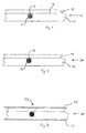
- Figure 1 illustrates in cross sectional view part of a first embodiment of a flexible optical backplane;
- Figure 2 illustrates in cross sectional view part of a second embodiment of a flexible optical backplane;
- Figure 3 illustrates in cross sectional view a rigid optical backplane according to the present invention;
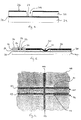
- Figure 4 illustrates in cross sectional view the formation of a channel within a layer of polyimide using a stop layer;
- Figure 5 illustrates, in cross section view the formation of an optical fibre crossover region of a backplate according to the present invention, within a layer of polyimide using a further stop layer;
- Figure 6 illustrates in plan view an enlarged channel localised to the crossover region;
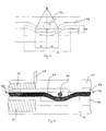
- Figure 7 illustrates in cross sectional diagrammatic view a technique for the calculation of the minimum radius for an optical fibre to bend under another optical fibre in the crossover region;
- Figure 8 illustrates in cross sectional view the formation of a ribbon enclosing an optical fibre;
- Figure 9 illustrates in cross sectional view, normal to the longitudinal axis of the ribbon, the optical fibres in position for connection with an optical fibre interconnector;
- Figure 10 illustrates in plan view the layout of optical fibres within the plane of the optical backplane, and
- Fibre 11 illustrates in plan view the layout of channels within the plane of the polyimide layer.
-
- In Figure 1, there is illustrated part of a first embodiment of the present invention including a first layer 10 formed from a polyimide material with a channel 11 defined in the polyimide with the plane of the layer 10 and an
optical fibre 12 located within the channel 11. The defining of the channel 11 will be described with reference to Figures 4 and 5 below. Afurther layer 13 also formed of polyimide material is bonded to layer 10 withepoxy resin 14 and pressure applied over the plane of thelayers 10 and 13, in this manner aflexible structure 15 is constructed. - An alternative to the construction described with reference to Figure 1 is illustrated in Figure 2 in which is shown in part a second embodiment comprising a
first layer 16 formed from a polyimide material with achannel 17 defined in the polyimide with the plane of thelayer 16 and optical onfibre 18 located within thechannel 17. The defining of thechannel 17 will be described with reference to Figures 4 and 5 below. Afurther layer 19 formed of a curing type material, such as a low temperature (85°C) epoxy resin, is applied under pressure over the plane of thelayer 16, in this manner an alternativeflexible structure 20 is constructed. - It will be appreciated that the
flexible structure 20 when described below could be readily replaced by theflexible structure 15 and that the description will only refer to theflexible structure 20 for clarity. - When the optical backplane is to be used in conjunction with the passive and/or active components the
flexible structures 15 to 20 are made rigid to provide a stable base to which to attach the components. In Figure 3, there is illustrated aflexible structure 20, wherein theflexible structure 20 is bonded to alayer 21 of epoxy glass FR4 on one side of the plane of theflexible structure 20 with an epoxy resin. Bonding of thelayer 21 to theflexible structure 20 provides rigidity to theflexible structure 20. Further rigidity for theflexible structure 20 is provided by bonding afurther layer 22 of epoxy glass FR4 to the opposite side of theflexible structure 20 with epoxy resin. In this manner a rigid structure 23 is constructed. - Passive or active components can be secured to the structure 23 and/or interconnected with optical fibres and optical components within the optical backplane in accordance with conventional printed circuit board and optical connection techniques. The external surfaces of the
layers layers layers layers flexible structure 20. Apertures can be provided between and/or in layers to enable connection of these components to the optical fibres. In the case of active components power is provided using conventional printed circuit board technology. - In Figure 4, a
channel 24 is formed in apolyimide layer 25 using an Excimer laser in accordance with one of the two following methods. A polyimide layer having acopper mask 26 transposed thereon is exposed to an Excimer laser passing over exposed portions provided by thecopper mask 26, in either a time based or number of passes fashion, to ablated the polyimide and form the channel. Alternatively, as illustrated in Figure 4, thechannel 24 is defined in thepolyimide layer 25 by transposing acopper mask 26 on the surface of thepolyimide layer 25 and exposing the etched portions to an Excimer laser to ablated thepolyimide layer 25 and form thechannel 24. Thebase 27 of thechannel 24 is defined by acopper stop layer 28 which prevents the Excimer laser machining further. - When a
channel 24 with greater depth in localised areas is required, further ablation with the Excimer laser will remove thestop layer 28 to allow the Excimer laser to penetrate into afurther polyimide layer 29 thereby providing greater depth. - Greater depth is required for a
crossover region 30 as illustrated in Figure 5. Here a firstoptical fibre 31 is required to pass over a secondoptical fibre 32 so a greater depth is provided at the crossover point by ablating a first layer ofpolyimide 33 having acopper mask 34 with an Excimer laser. Ablation with the laser is halted by a firstcopper stop layer 35. The first process of ablation provideschannels 36 foroptical fibre 37 andoptical fibres crossover region 30, in thepolyimide layer 33. - In the
crossover region 30 thestop layer 35 is further exposed to the Excimer laser until it is burnt away and ablation of a second layer ofpolyimide 38 allows the necessary depth to provide thecrossover region 30 foroptical fibres crossover region 30 is defined by a secondcopper stop layer 39 to prevent penetration into afurther polyimide layer 40. - It will be noted that ablation can be achieved using any form of heat generating means.
- In Figure 6, two
crossover regions 41 are illustrated foroptical fibres channels polyimide layer 48. In thecrossover regions 41 thechannels optical fibres - In Figure 7, the bending of an
optical fibre 49 at a crossover region to pass under anotheroptical fibre 50 must not exceed a minimum recommended bend radius, for this application the bend radius of theoptical fibre 49 should be great than or equal to 10 millimetres. With reference to Figure 7, the theoretical bend radius can be calculated using the formula,optical fibre 49 underneathoptical fibre 50 and the distance between the core of theoptical fibre 49 from theoptical fibre 50, respectively
For example, given that the length of acrossover 51 is 7.3 millimetres and that a core bend deflection 52 is 0.15 millimetres then, - A further design rule, to reduce the cross talk and loss is to only intersect the optical fibres at right angles relative to one another.
- The
flexible structures ribbon 53 is formed as an integral part of aflexible structure 54 by forming a rigid structure from a layer ofpolyimide 55 having defining channels foroptical fibres epoxy resin layer 58 bonded to thepolyimide 55. As theribbon 53 will when formed be thinner than theflexible structure 54 it is necessary to machine thepolyimide layer 58 to provide an area to retain aspacer 59. Machining can be by way of ablation with Excimer laser of thepolyimide layer 55.Spacer 59 is coated with a layer of material which inhibits adhesion to thepolyimide layer 55. - The
flexible structure 54 is made rigid by bondingrigid layers flexible structure 54.Rigid layer 61 is also machined to co-operate withspacer 59. The area machined into therigid layer 61 will not bond to thespacer 59 as the spacer has been coated in a material which inhibits adhesion to therigid layer 61. - The
rigid layer 60 is also machined to provide an area to retain aspacer 62 between the machined area and theepoxy resin layer 58. Thespacer 62 is also coated with a layer of material which inhibits adhesion to either theepoxy resin 58 on therigid layer 60. - The
flexible structure 54 is bonded between therigid layers router machine bit 63 is used to cut through therigid layers spacers spacers flexible structure 54 in this region undamaged by the process. There is now provided theribbon 53 with anoptical fibre 57 therein. - A number of optical fibres can be enclosed in , a single ribbon, as illustrated in Figure 9. The
optical fibres 64 are laid in acommunal channel 65 defined in apolyimide layer 66 and bonded to anepoxy resin layer 67. Thepitch 68 between each core of adjacentoptical fibres 64 depends on the optimum pitch required for interconnection with an optical connector. In this case the pitch of theoptical fibres 64 are required to be 250 micrometers for the highest possible yield for connection. Since theoptical fibres 64 are 250 micrometers in diameter they are laid abutting one another in thecommunal channel 65. - When the optical fibres are laid in their respective channels as defined in the polyimide layer, the optical fibres can be retained, at least temporarily, in the channels using a rubber based adhesive such as cyanacrylate.
- Figure 10 illustrates the entire optical backplane with
flexible ribbons 69 extending from therigid backplane 70 and the exposed optical fibres 71 for interconnection with optical connectors. A number of fixingapertures 72 are also shown for securing the optical backplane to a racking system (not shown) - Figure 10 illustrates in
plan defining channels 73 in a polyimide layer.
Claims (44)
- An optical backplane having a first layer of material (10, 16, 25, 33, 38, 48), a stop layer (28, 35) disposed on the first layer, a second layer (29, 38) disposed on the stop layer (28, 35), at least two channels (11, 17, 24, 36, 45, 46, 47) defined within the plane of the first layer (10, 16, 25, 33, 48) and at least one optical fibre (12, 18, 31, 32, 37, 42, 43, 44) located within at least one of the channels (11, 17, 24, 36, 45, 46, 47), wherein at least two of the channels (46, 47) intersect in a crossover region (30, 41) and one of these channels (46) is formed deeper at the crossover point extending into the second layer (29, 38) so as to permit the optical fibre (43) located in that channel (46) to cross underneath an optical fibre (44) located within the other channel (47).
- An optical backplane, as claimed in Claim 1, having a base (27) for at least one of the channels (24), which base (27) is defined by the stop layer (28).
- An optical backplane, as claimed in any preceding claim, in which optical fibre (12) is laid in its channel (11) and retained in position with an adhesive.
- An optical backplane, as claimed in any preceding claim, in which a bend in at least one channel (11, 17, 24, 36, 45, 46, 47) has a radius greater than 10mm.
- An optical backplane, as claimed in any one of Claims 1 to 4, in which the two channels (46, 47) intersect substantially at right angles in the crossover region (41).
- An optical backplane, as claimed in any one of Claims 1 to 5, in which the channels (46, 47) are locally widened at the crossover region.
- An optical backplane, as claimed in Claim 6, in which the locally widened portion of the channels (46, 47) is filled with a set resin.
- An optical backplane, as claimed in any one of Claims 1 to 7, in which a base for the deeper formed channel in the crossover region (30) is defined by a stop layer (39).
- An optical backplane, as claimed in any preceding claim, including a further layer of material (19) bonded to the first layer (10) to enclose the optical fibre (12).
- An optical backplane, as claimed in Claim 9, in which the further layer of material (19) is formed from a cured resin which extends into the channel (11) to enclose each optical fibre (12).
- An optical backplane, as claimed in Claim 9 or Claim 10, in which the material (10, 19) is formed from polyimide.
- An optical backplane, as claimed in any one of Claims 9 to 11, in which layers (10, 19) form a flexible structure (20).
- An optical backplane, as claimed in Claim 12, including a rigid layer (21) bonded to one side of the flexible structure (20) to provide a rigid structure.
- An optical backplane, as claimed in Claim 13, including a further rigid layer (22) bonded to the reverse side of the flexible structure (20).
- An optical backplane, as claimed in Claim 13 or Claim 14 in which the rigid layers (21, 22) are formed from epoxy glass resin.
- An optical backplane, as claimed in any one of Claims 12 to 15, in which the layers (10, 19, 21, 22) are bonded by an epoxy resin.
- An optical backplane, as claimed in any of Claims 13 to 16, in which the layers (10, 19, 21, 22) have at least one aperture containing an optical component connected to at least one of the optical fibres (12).
- An optical backplane, as claimed in any one of Claims 13 to 17, in which the layers (10, 19, 21, 22) have at least one aperture containing an electro-optical component connected to at least one of the optical fibres (12).
- An optical backplane, as claimed in Claim 17 or Claim 18, in which each aperture is filled with a set resin.
- An optical backplane, as claimed in any one of Claims 13 to 19, including a printed circuit carried by a surface of at least one of the layers (10, 19, 21, 22).
- An optical backplane, as claimed in Claim 20, in which at least one of the layers (10, 19, 21, 22) has at least one aperture containing a component connected to the printed circuit.
- An optical backplane, as claimed in Claim 21, in which each aperture is filled with a set resin.
- An optical backplane, as claimed in any one of Claims 14 to 22, in which the flexible structure (20) extends beyond the rigid layer (21, 22) to define a flexible optical ribbon (69).
- An optical backplane, as claimed in Claim 23, in which the flexible optical ribbon (69) terminates in an optical connector, and at least one optical fibre (64) is located in a communal channel (65) immediately adjacent the optical connector.
- An optical backplane, as claimed in Claim 24, in which the optical fibre (64) is located in laterally spaced individual channels which converge into the communal channel (65).
- A method of manufacturing an optical backplane including forming at least two channels (11, 17, 24, 36, 45, 46, 47) within the plane of a first layer of material (10, 16, 25, 33, 38, 48) disposing a stop layer (28, 35) on the first layer, disposing a second layer (29, 38) on the stop layer (28. 35), and locating at least one optical fibre (12, 18, 31, 32, 37, 42, 43, 44) within at least one of the channels (11, 17, 24, 36, 45, 46, 47), including defining a crossover region (30, 41) for at least two of the channels (46, 47) by forming one of these channels (46) deeper at the crossover point and extending into the second layer (29, 38) so as to permit the optical fibre (43) located in that channel (46) to cross underneath an optical fibre (44) located within the other channel (47).
- A method, as claimed in Claim 26, including forming at least one of the channels (24) by ablating the first layer of material (25).
- A method, as claimed in Claim 27, including using a mask (26) superimposed over the layer (25) to expose only those areas of the first layer of material (25) that are to be ablated.
- A method, as claimed in Claim 27 or Claim 28, including using an Excimer laser to ablate the first layer of material (25).
- A method, as claimed in any one of Claims 27 to 29, including using a stop layer (28) to define a base (27) of at least one of the channels (24).
- A method, as claimed in any one of Claims 26 to 30, including laying each optical fibre (12) in its channel (11) and applying an adhesive between each optical fibre (12) and its channel (11).
- A method, as claimed in any one of Claims 26 to 31, including forming a bend in at least one channel (11, 17, 24, 36, 45, 46, 47) with a radius greater than 10mm.
- A method, as claimed in any one of Claims 26 to 32, including forming channels (45, 46) such that they are locally wider in the crossover region (41).
- A method, as claimed in Claim 33, including filling the locally widened portion of the channels (45, 46) with a setting resin.
- A method, as claimed in any one of Claims 26 to 34, including bonding a further layer of material (19) to the layer (10) to enclose each optical fibre (12).
- A method, as claimed in Claim 35, in which the layers (10, 19) form a flexible structure (20), including bonding a rigid layer (21) to one side of the flexible structure (20).
- A method, as claimed in Claim 36, including bonding a further rigid layer (22) to the reverse side of the flexible structure (20).
- A method, as claimed in any one of Claims 35 to 37, including introducing an epoxy resin between layers (10, 19, 21, 22) and bonding them to together under pressure over a surface area of the layers (10, 19, 21, 22).
- A method, as claimed in Claims 36 or 37, including forming at least one aperture in at least one of the layers of material (10, 19, 21, 22), positioning an optical component within the aperture and connecting that component to at least one of the optical fibres (12).
- A method, as claimed in any one of Claims 36 to 39, including forming at least one aperture in at least one of the layers of material (10, 19, 21, 22), positioning an electro-optical component within the aperture and connecting that component to at least one of the optical fibres (12).
- A method, as claimed in any one of Claims 36 to 40, including forming a printed circuit on a surface of at least one of the layers of material (10, 19, 21, 22).
- A method, as claimed in Claim 41, including forming at least one aperture in at least one of the layers of material (10, 19, 21, 22), positioning a component within the aperture and connecting that component to the printed circuit.
- A method, as claimed in any one of Claims 36 to 42, including spacing at least one rigid layer (60, 61) from the flexible structure (54) to which it is to bond with spacer material (59, 62) in specified regions and using a bond inhibiting agent to prevent bonding of the spacer material (59, 62) to either the rigid layer (60, 61) or to the flexible structure (54), and then removing that portion of the rigid layer (60, 61) in the specified regions to expose those portions of the flexible structure (53).
- A method, as in Claim 43, including defining each channel in the exposed portions of the flexible structure (53) such that the pitch between optical fibres enables interconnection with a multi way ribbon connector.
Applications Claiming Priority (2)
| Application Number | Priority Date | Filing Date | Title |
|---|---|---|---|
| GB9612401 | 1996-06-13 | ||
| GB9612401A GB2314214B (en) | 1996-06-13 | 1996-06-13 | Optical backplane |
Publications (2)
| Publication Number | Publication Date |
|---|---|
| EP0813083A1 EP0813083A1 (en) | 1997-12-17 |
| EP0813083B1 true EP0813083B1 (en) | 2005-08-10 |
Family
ID=10795250
Family Applications (1)
| Application Number | Title | Priority Date | Filing Date |
|---|---|---|---|
| EP97304167A Expired - Lifetime EP0813083B1 (en) | 1996-06-13 | 1997-06-13 | Fexible optical backplane |
Country Status (4)
| Country | Link |
|---|---|
| US (1) | US5937133A (en) |
| EP (1) | EP0813083B1 (en) |
| DE (1) | DE69733920T2 (en) |
| GB (1) | GB2314214B (en) |
Families Citing this family (31)
| Publication number | Priority date | Publication date | Assignee | Title |
|---|---|---|---|---|
| JPH11183749A (en) | 1997-12-22 | 1999-07-09 | Hitachi Chem Co Ltd | Optical circuit board and manufacture therefor |
| CA2323481C (en) * | 1998-03-12 | 2005-01-11 | Tomoegawa Paper Co., Ltd. | Optical connection component and method of producing the same |
| US6381396B1 (en) * | 1999-12-08 | 2002-04-30 | Molex Incorporated | Optical interconnection apparatus |
| US7058245B2 (en) * | 2000-04-04 | 2006-06-06 | Waveguide Solutions, Inc. | Integrated optical circuits |
| JP2002303737A (en) * | 2001-01-24 | 2002-10-18 | Mitsubishi Cable Ind Ltd | Optical fiber wiring board |
| US6547445B2 (en) * | 2001-02-06 | 2003-04-15 | Teradyne, Inc. | High-density fiber optic backplane |
| US6587630B2 (en) * | 2001-06-01 | 2003-07-01 | Sycamore Networks, Inc. | Optical backplane cartridge |
| US6623177B1 (en) | 2001-07-09 | 2003-09-23 | Emc Corporation | Systems and methods for providing fiber optic communications between circuit boards |
| US6850684B2 (en) * | 2001-08-10 | 2005-02-01 | 3M Innovative Properties Company | Three dimensional optical circuits |
| US6556754B2 (en) | 2001-08-10 | 2003-04-29 | 3M Innovative Properties Company | Three dimensional optical circuit |
| US6690867B2 (en) | 2001-08-31 | 2004-02-10 | Corning Cable Systems Llc | Optical interconnect assemblies and methods therefor |
| US6587631B2 (en) | 2001-12-04 | 2003-07-01 | Harris Corporation | Fiber-optic backplane method and apparatus |
| US7532782B2 (en) * | 2002-04-18 | 2009-05-12 | Pivotal Decisions Llc | Flexible optical circuit apparatus and method |
| US6839935B2 (en) | 2002-05-29 | 2005-01-11 | Teradyne, Inc. | Methods and apparatus for cleaning optical connectors |
| US6762941B2 (en) | 2002-07-15 | 2004-07-13 | Teradyne, Inc. | Techniques for connecting a set of connecting elements using an improved latching apparatus |
| US6848841B2 (en) | 2002-09-09 | 2005-02-01 | Hewlett-Packard Development Company, L.P. | Optical component connector |
| US6832858B2 (en) | 2002-09-13 | 2004-12-21 | Teradyne, Inc. | Techniques for forming fiber optic connections in a modularized manner |
| JP4334211B2 (en) * | 2002-12-25 | 2009-09-30 | スリーエム イノベイティブ プロパティズ カンパニー | Optical wiring sheet |
| US7042562B2 (en) | 2002-12-26 | 2006-05-09 | Amphenol Corp. | Systems and methods for inspecting an optical interface |
| CN100356219C (en) * | 2005-11-30 | 2007-12-19 | 武汉海博光技术有限公司 | Method for manufacturing FR4 optical fiber network back plate |
| US20070154156A1 (en) * | 2005-12-30 | 2007-07-05 | Gary Brist | Imprinted waveguide printed circuit board structure |
| US7454097B2 (en) * | 2006-03-31 | 2008-11-18 | Xyratex Technology Limited | Optical circuit board, an optical backplane and an optical communication system |
| US7587115B1 (en) | 2006-11-30 | 2009-09-08 | Lockheed Martin Corporation | Integrated functionality in optical backplane |
| JP5495623B2 (en) * | 2008-06-18 | 2014-05-21 | キヤノン株式会社 | Substrate processing method, liquid discharge head substrate manufacturing method, and liquid discharge head manufacturing method |
| US9757639B2 (en) | 2009-11-24 | 2017-09-12 | Seth E. Eisner Trust | Disparity correction for location-aware distributed sporting events |
| JP6079122B2 (en) * | 2012-10-12 | 2017-02-15 | 日立金属株式会社 | Optical substrate, optical substrate manufacturing method, and optical module structure |
| JP5929716B2 (en) * | 2012-11-09 | 2016-06-08 | 日立金属株式会社 | Optical substrate, optical substrate manufacturing method, and optical module |
| US10888011B2 (en) | 2014-10-27 | 2021-01-05 | Hewlett Packard Enterprise Development Lp | Modular apparatuses and system for backplane connections |
| US10234644B1 (en) * | 2017-10-20 | 2019-03-19 | Corning Optical Communications LLC | Optical-electrical printed circuit boards with integrated optical waveguide arrays and photonic assemblies using same |
| WO2019171700A1 (en) * | 2018-03-07 | 2019-09-12 | 住友電気工業株式会社 | Optical wiring member and optical wiring structure |
| CN116520519B (en) * | 2023-04-07 | 2024-03-19 | 合肥比洋通信科技有限公司 | OXC all-optical backboard |
Family Cites Families (11)
| Publication number | Priority date | Publication date | Assignee | Title |
|---|---|---|---|---|
| GB2156604B (en) * | 1984-03-22 | 1987-12-23 | Porta Systems Corp | Telephone connector block |
| JPS62123406A (en) * | 1985-11-22 | 1987-06-04 | Furukawa Electric Co Ltd:The | Optical wiring board |
| US4943136A (en) * | 1988-12-09 | 1990-07-24 | The Boeing Company | Optical backplane interconnection |
| GB9014639D0 (en) * | 1990-07-02 | 1990-08-22 | British Telecomm | Optical component packaging |
| US5144691A (en) * | 1990-07-20 | 1992-09-01 | Cray Research, Inc. | Computer signal interconnect apparatus |
| US5155785A (en) * | 1991-05-01 | 1992-10-13 | At&T Bell Laboratories | Optical fiber interconnection apparatus and method |
| US5204925A (en) * | 1991-09-11 | 1993-04-20 | At&T Bell Laboratories | Optical interconnection of circuit packs |
| DE4309279A1 (en) * | 1993-03-23 | 1994-09-29 | Sel Alcatel Ag | Method for producing an optical fibre coupling |
| US5425831A (en) * | 1994-03-18 | 1995-06-20 | At&T Corp. | Optical fiber connecting method |
| GB2292466B (en) * | 1994-08-15 | 1997-09-10 | Pirelli General Plc | Guiding optical fibres in ducts |
| TW281731B (en) * | 1994-08-26 | 1996-07-21 | Akzo Nobel Nv |
-
1996
- 1996-06-13 GB GB9612401A patent/GB2314214B/en not_active Expired - Fee Related
-
1997
- 1997-06-13 EP EP97304167A patent/EP0813083B1/en not_active Expired - Lifetime
- 1997-06-13 DE DE69733920T patent/DE69733920T2/en not_active Expired - Lifetime
- 1997-06-13 US US08/874,234 patent/US5937133A/en not_active Expired - Fee Related
Also Published As
| Publication number | Publication date |
|---|---|
| GB2314214B (en) | 2000-09-20 |
| DE69733920D1 (en) | 2005-09-15 |
| US5937133A (en) | 1999-08-10 |
| GB9612401D0 (en) | 1996-08-14 |
| DE69733920T2 (en) | 2006-04-13 |
| GB2314214A (en) | 1997-12-17 |
| EP0813083A1 (en) | 1997-12-17 |
Similar Documents
| Publication | Publication Date | Title |
|---|---|---|
| US5937133A (en) | Optical backplanes | |
| KR101390137B1 (en) | Optical waveguide substrate having positioning structure, method for manufacturing same, and method for manufacturing opto-electric hybrid substrate | |
| KR100456121B1 (en) | Manufacturing method of multilayer substrate and multilayer substrate produced by the manufacturing method | |
| EP1019764B1 (en) | Flexible optical interconnections | |
| US20240385366A1 (en) | Optical waveguide device | |
| GB2340959A (en) | Multilayered optoelectronic circuit board with transparent layers | |
| EP1219991B1 (en) | Polarization-maintaining fiber ribbon termination | |
| KR20080100131A (en) | Optical waveguide, its manufacturing method, and manufacturing method of opto-electric hybrid substrate | |
| CN116033651B (en) | Circuit board and its manufacturing method | |
| WO2005040881A1 (en) | Multi-layer optical circuit and method for making | |
| Brusberg et al. | Large optical backplane with embedded graded-index glass waveguides and fiber-flex termination | |
| US7555176B2 (en) | Method for producing an optical splitter, and optical splitter | |
| JP2010170150A (en) | Method of manufacturing printed circuit board | |
| WO2009001119A1 (en) | Microwave circuit assembly | |
| KR20060060733A (en) | Fiber Optics Embedded in Printed Circuit Boards | |
| DE60028761T2 (en) | DEVICE FOR OPTICAL CONNECTION | |
| JP7185165B2 (en) | optical waveguide chip | |
| TWI846070B (en) | Method for manufacturing multilayer circuit board and multilayer circuit board | |
| KR20020095866A (en) | Optical fiber array | |
| JP4074563B2 (en) | Manufacturing method of optical fiber guide parts | |
| KR20040057154A (en) | A method for forming multi-layer PCB for optical-waveguides | |
| JP2006011179A (en) | Film optical waveguide manufacturing method and manufacturing apparatus | |
| EP2054746B1 (en) | Method for producing an optical splitter and optical splitter | |
| JP4329742B2 (en) | Optical fiber sheet manufacturing method and optical fiber pre-sheet manufacturing method | |
| JP4683859B2 (en) | Pattern forming method on side of optical fiber |
Legal Events
| Date | Code | Title | Description |
|---|---|---|---|
| PUAI | Public reference made under article 153(3) epc to a published international application that has entered the european phase |
Free format text: ORIGINAL CODE: 0009012 |
|
| AK | Designated contracting states |
Kind code of ref document: A1 Designated state(s): BE DE FR GB IT NL SE |
|
| 17P | Request for examination filed |
Effective date: 19980611 |
|
| AKX | Designation fees paid |
Free format text: BE DE FR GB IT NL SE |
|
| RBV | Designated contracting states (corrected) |
Designated state(s): BE DE FR GB IT NL SE |
|
| RAP1 | Party data changed (applicant data changed or rights of an application transferred) |
Owner name: BAE SYSTEMS ELECTRONICS LTD. |
|
| 17Q | First examination report despatched |
Effective date: 20031113 |
|
| GRAP | Despatch of communication of intention to grant a patent |
Free format text: ORIGINAL CODE: EPIDOSNIGR1 |
|
| GRAS | Grant fee paid |
Free format text: ORIGINAL CODE: EPIDOSNIGR3 |
|
| GRAA | (expected) grant |
Free format text: ORIGINAL CODE: 0009210 |
|
| AK | Designated contracting states |
Kind code of ref document: B1 Designated state(s): BE DE FR GB IT NL SE |
|
| PG25 | Lapsed in a contracting state [announced via postgrant information from national office to epo] |
Ref country code: NL Free format text: LAPSE BECAUSE OF FAILURE TO SUBMIT A TRANSLATION OF THE DESCRIPTION OR TO PAY THE FEE WITHIN THE PRESCRIBED TIME-LIMIT Effective date: 20050810 Ref country code: BE Free format text: LAPSE BECAUSE OF FAILURE TO SUBMIT A TRANSLATION OF THE DESCRIPTION OR TO PAY THE FEE WITHIN THE PRESCRIBED TIME-LIMIT Effective date: 20050810 |
|
| REG | Reference to a national code |
Ref country code: GB Ref legal event code: FG4D |
|
| REF | Corresponds to: |
Ref document number: 69733920 Country of ref document: DE Date of ref document: 20050915 Kind code of ref document: P |
|
| REG | Reference to a national code |
Ref country code: SE Ref legal event code: TRGR |
|
| REG | Reference to a national code |
Ref country code: GB Ref legal event code: 732E |
|
| NLV1 | Nl: lapsed or annulled due to failure to fulfill the requirements of art. 29p and 29m of the patents act | ||
| REG | Reference to a national code |
Ref country code: FR Ref legal event code: TP |
|
| ET | Fr: translation filed | ||
| PLBE | No opposition filed within time limit |
Free format text: ORIGINAL CODE: 0009261 |
|
| STAA | Information on the status of an ep patent application or granted ep patent |
Free format text: STATUS: NO OPPOSITION FILED WITHIN TIME LIMIT |
|
| 26N | No opposition filed |
Effective date: 20060511 |
|
| PGFP | Annual fee paid to national office [announced via postgrant information from national office to epo] |
Ref country code: FR Payment date: 20100706 Year of fee payment: 14 |
|
| PGFP | Annual fee paid to national office [announced via postgrant information from national office to epo] |
Ref country code: IT Payment date: 20100626 Year of fee payment: 14 |
|
| PGFP | Annual fee paid to national office [announced via postgrant information from national office to epo] |
Ref country code: SE Payment date: 20100614 Year of fee payment: 14 Ref country code: GB Payment date: 20100618 Year of fee payment: 14 Ref country code: DE Payment date: 20100625 Year of fee payment: 14 |
|
| REG | Reference to a national code |
Ref country code: SE Ref legal event code: EUG |
|
| GBPC | Gb: european patent ceased through non-payment of renewal fee |
Effective date: 20110613 |
|
| PG25 | Lapsed in a contracting state [announced via postgrant information from national office to epo] |
Ref country code: IT Free format text: LAPSE BECAUSE OF NON-PAYMENT OF DUE FEES Effective date: 20110613 |
|
| REG | Reference to a national code |
Ref country code: FR Ref legal event code: ST Effective date: 20120229 |
|
| REG | Reference to a national code |
Ref country code: DE Ref legal event code: R119 Ref document number: 69733920 Country of ref document: DE Effective date: 20120103 |
|
| PG25 | Lapsed in a contracting state [announced via postgrant information from national office to epo] |
Ref country code: DE Free format text: LAPSE BECAUSE OF NON-PAYMENT OF DUE FEES Effective date: 20120103 Ref country code: FR Free format text: LAPSE BECAUSE OF NON-PAYMENT OF DUE FEES Effective date: 20110630 |
|
| PG25 | Lapsed in a contracting state [announced via postgrant information from national office to epo] |
Ref country code: GB Free format text: LAPSE BECAUSE OF NON-PAYMENT OF DUE FEES Effective date: 20110613 |
|
| PG25 | Lapsed in a contracting state [announced via postgrant information from national office to epo] |
Ref country code: SE Free format text: LAPSE BECAUSE OF NON-PAYMENT OF DUE FEES Effective date: 20110614 |