EP0813070A2 - Capteur magnétique muni d'un multivibrateur CMOS - Google Patents
Capteur magnétique muni d'un multivibrateur CMOS Download PDFInfo
- Publication number
- EP0813070A2 EP0813070A2 EP97109476A EP97109476A EP0813070A2 EP 0813070 A2 EP0813070 A2 EP 0813070A2 EP 97109476 A EP97109476 A EP 97109476A EP 97109476 A EP97109476 A EP 97109476A EP 0813070 A2 EP0813070 A2 EP 0813070A2
- Authority
- EP
- European Patent Office
- Prior art keywords
- magneto
- cmos inverters
- impedance element
- cmos
- magnetic sensor
- Prior art date
- Legal status (The legal status is an assumption and is not a legal conclusion. Google has not performed a legal analysis and makes no representation as to the accuracy of the status listed.)
- Granted
Links
- 230000005291 magnetic effect Effects 0.000 title claims abstract description 63
- 239000003990 capacitor Substances 0.000 claims abstract description 19
- 230000007704 transition Effects 0.000 claims abstract description 11
- 238000001514 detection method Methods 0.000 claims description 26
- 230000004888 barrier function Effects 0.000 claims description 4
- 230000002500 effect on skin Effects 0.000 abstract description 5
- 230000010355 oscillation Effects 0.000 description 14
- 230000004044 response Effects 0.000 description 8
- 238000010586 diagram Methods 0.000 description 7
- 230000035945 sensitivity Effects 0.000 description 7
- 230000003247 decreasing effect Effects 0.000 description 5
- 230000007423 decrease Effects 0.000 description 4
- 230000000694 effects Effects 0.000 description 4
- 230000005284 excitation Effects 0.000 description 3
- 230000004907 flux Effects 0.000 description 3
- 239000000696 magnetic material Substances 0.000 description 3
- 230000000295 complement effect Effects 0.000 description 2
- 238000007689 inspection Methods 0.000 description 2
- 238000005259 measurement Methods 0.000 description 2
- 230000004043 responsiveness Effects 0.000 description 2
- 229920006395 saturated elastomer Polymers 0.000 description 2
- 239000010409 thin film Substances 0.000 description 2
- 230000001133 acceleration Effects 0.000 description 1
- 230000002411 adverse Effects 0.000 description 1
- 230000033228 biological regulation Effects 0.000 description 1
- 238000010622 cold drawing Methods 0.000 description 1
- 238000001816 cooling Methods 0.000 description 1
- 230000004069 differentiation Effects 0.000 description 1
- 238000006073 displacement reaction Methods 0.000 description 1
- 239000003814 drug Substances 0.000 description 1
- 238000005516 engineering process Methods 0.000 description 1
- 230000005669 field effect Effects 0.000 description 1
- 238000010438 heat treatment Methods 0.000 description 1
- 230000005415 magnetization Effects 0.000 description 1
- 238000000034 method Methods 0.000 description 1
- 230000004048 modification Effects 0.000 description 1
- 238000012986 modification Methods 0.000 description 1
- 230000002265 prevention Effects 0.000 description 1
- 238000004544 sputter deposition Methods 0.000 description 1
Images


Classifications
-
- G—PHYSICS
- G01—MEASURING; TESTING
- G01R—MEASURING ELECTRIC VARIABLES; MEASURING MAGNETIC VARIABLES
- G01R33/00—Arrangements or instruments for measuring magnetic variables
- G01R33/02—Measuring direction or magnitude of magnetic fields or magnetic flux
- G01R33/06—Measuring direction or magnitude of magnetic fields or magnetic flux using galvano-magnetic devices
- G01R33/09—Magnetoresistive devices
Definitions
- the present invention relates to compact low-power consumption type magnetic sensors having high sensitivity and high response speed. More particularly, the present invention relates to high-performance micro magnetic sensors such as magnetic recording heads for computers and information devices; magnetic sensor heads for rotary encoders; and magnetic sensor heads that are used in factory automation so as to carry out measurement for physical distribution, nondestructive magnetic inspection, etc.
- a micro-dimensioned head of a Hall element or MR element can be used.
- the sensitivity of such a head is insufficient.
- a flux gate sensor is used for such purpose, sufficient response speed cannot be obtained.
- the flux gate sensor also has a problem that its sensitivity becomes quite insufficient when formed in a micro-sized head.
- MI magneto-impedance
- a micro-dimensioned head utilizing the improved MI element has a resolution of one microgauss and a high responsiveness of 1 MHz, thereby covering a large portion of the required range for magnetic field detection.
- the power consumption of the micro-dimensioned head is as low as about 30 - 50 mW.
- MI micro sensor is a high performance sensor having a resolution of one microgauss and a high responsiveness of 1 MHz, it can solve many of the technical problems related to new types of magnetic detection required in many industrial fields.
- MR elements, Hall elements, and flux gate sensors which have been widely used, are expected to be replaced with MI elements in the near future so as to realize more advanced systems.
- Another problem is difficulty in designing a sensor circuit and stems from the necessity of high-frequency technology. Another problem is power consumption in the case where many MI elements are used.
- the former problem has been basically solved through use of a high-frequency oscillation type magnetic head in which the magnetic head is driven by means of a Colpitts oscillation circuit or a multivibrator circuit.
- the power consumption of a single MI element available at the present is about 30 - 50 mW, and this is sufficiently low for the element itself.
- the maximum allowable power consumption of the MI element is considered to be further decreased (for example, to be less than 1 mW).
- an object of the present invention is to provide a stable and low power consumption magnetic sensor, in which a complementary MOSFET (CMOS) oscillation circuit is used as a sensor circuit so as to sufficiently excite an MI element such as an amorphous wire through use of a sharp pulse current in a transition state of CMOS inverters, while maintaining the excitation current at zero in the remaining period by utilizing the characteristics of the CMOS inverters, which causes no current flow in a steady state.
- CMOS complementary MOSFET
- the present invention provides a magnetic sensor which includes a DC power source, a multivibrator circuit composed of two CMOS inverters, a resistor, and a capacitor, each of the CMOS inverters being composed of a pMOS transistor and an nMOS transistor connected in series, and a magneto-impedance element (hereinafter referred to as an "MI element").
- MI element magneto-impedance element
- the multivibrator circuit is of a self-oscillation type. More preferably, the multivibrator circuit is an astable multivibrator circuit.
- a Schottky barrier diode and a detection circuit are connected to the output terminal of the MI element so as to yield a dc output voltage.
- the present invention also provides a magnetic sensor which includes a first multivibrator circuit composed of a first pair of CMOS inverters, a first MI element, a first resistor, and a first capacitor, each of the CMOS inverters being composed of a pMOS transistor and an nMOS transistor connected in series; a second multivibrator circuit composed of a second pair of CMOS inverters, a second MI element, a second resistor, and a second capacitor, each of the CMOS inverters being composed of a pMOS transistor and an nMOS transistor connected in series; and a differential amplifier circuit connected to the first and second multivibrator circuits so as to output a voltage corresponding to the difference between the outputs of the first and second multivibrator circuits.
- the magnetic sensor according to the present invention has the following advantages.
- the magnetic sensor of the present invention can be used for detection of weak high-frequency magnetic fields, for accurate detection of a direction or angle, for detection of displacement, velocity, or acceleration in cooperation with a micro magnet.
- Pulse magnetization of MI elements is also carried out with differentiation of the rectangular output voltage of the CMOS multivibrator, in which the pulsed voltage is reinforced through an inverter and then applied to the MI elements.
- Biasing or setting the operating point of the MI element is carried out applying a dc magnetic field along with the MI element length direction, or applying the same pulse current to a coil set around the MI element through which the pulse current is applied.
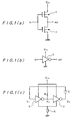
- FIGS. 1A - 1C show basic circuits that constitute an MI micro sensor that uses a multivibrator oscillation circuit formed of CMOS inverters, wherein FIG. 1A shows a CMOS inverter circuit (a NOT circuit); FIG. 1B shows a gate symbol for NOT logic; and FIG. 1C is a basic circuit of the MI micro sensor in which the inverter shown in FIGS. 1A and 1B is utilized.
- FIG. 1A shows a CMOS inverter circuit (a NOT circuit)
- FIG. 1B shows a gate symbol for NOT logic
- FIG. 1C is a basic circuit of the MI micro sensor in which the inverter shown in FIGS. 1A and 1B is utilized.
- each of the CMOS inverters 3 is composed of a pMOS FET 1 and an nMOS FET 2 connected serially.
- an MI element 5 is interposed between the CMOS inverters 3 and the ground.
- the MI element 5 may be interposed between a DC power source V CC and the CMOS inverters 3.
- a sharp pulse current having a pulse width of a few nanoseconds flows through the MI element 5 during transition periods when the CMOS inverters 3 turn ON or OFF.
- the inverters of the multivibrator circuit perform their switching operations as follows.
- the pMOS FET 1 turns OFF while the nMOS FET 2 turns ON (a saturated state).
- the pMOS FET 1 turns ON (a saturated state) while the nMOS FET 2 turns OFF.
- the threshold voltage V th is 30 - 60% of the DC power source voltage V CC .
- the multivibrator circuit immediately after the voltages V 1 and V 0 become V CC and the voltage V 2 becomes zero, current flows from the power source to the ground via the right-side inverter 3, the capacitor C, the resistor R, and the left-side inverter 3, in this order, so that the capacitor C is charged and the voltage V 1 decreases from the V CC toward zero at a rate corresponding to the CR time constant.
- the voltage V 1 reaches the threshold voltage V th
- the left-side CMOS inverter 3 changes its state so that the voltage V 2 becomes V CC
- the right-side inverter 3 changes its state so that the voltage V 0 becomes zero.
- the voltage V 0 having a square waveform in which voltage changes are repeated between the V CC and zero at a frequency of about (1/2.2) ⁇ CR.
- one of the pMOS FET 1 and the nMOS FET 2 is inevitably in the OFF state during a steady state operation between a certain switching operation and a subsequent switching operation of the CMOS inverter 3, and the current flowing from the power source is maintained at zero during such a steady state.
- the pMOS FET 1 and the nMOS FET 2 both turn ON (an unsaturated state) within a short period of a few nanoseconds, so that a sharp pulse current flows through the CMOS inverter 3.
- the circuit is designed such that the pulse current flows through MI element 5 such as an amorphous wire, the MI element 5 can exhibit a magneto-impedance effect stemming from the skin effect.
- electrical power is consumed only during a short period of a few nanoseconds within each period of the multivibrator oscillation. Therefore, the power consumption of the micro sensor is extremely low.
- MI element 5 there can be used a micro-dimensioned MI element disclosed in Japanese Patent Application Laid-Open ( kokai ) No. 7-181239.
- the MI element 5 examples include a thin elongated magnetic material, such as amorphous wire, having a diameter of 20 - 50 ⁇ m, and an amorphous magnetic thin film having a thickness of 1 - 4 ⁇ m.
- a pulse current produced due to transition of the CMOS inverters flows through the MI element 5, the MI element exhibits the skin effect, so that there can be obtained the magneto-impedance effect in which the impedance of the MI element increases sensitively in response to an external magnetic field Hex applied to the magnetic material in the longitudinal direction thereof.
- the pulse width (5 - 8 nanoseconds) of the pulse current produced due to transition of the CMOS inverter 3 does not depend on the oscillation frequency f ⁇ 0.45/CR, the MI effect or the magnetic field detection sensitivity is substantially constant regardless of the oscillation frequency.
- the average value of current flowing through the sensor within each oscillation period decreases, so that the power consumption can be decreased without decreasing the magnetic field detection sensitivity.
- a sharp pulse current produced due to transition of the CMOS inverters is applied to the MI element. This makes it a high performance magnetic sensor which has high sensitivity and high response speed and which consumes an extremely small amount of electrical power.
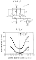
- FIG. 2 shows a circuit diagram of a CMOS MI sensor for a rotary encoder according to a second embodiment of the present invention.
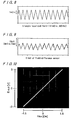
- FIG. 3A shows the output voltage of the CMOS MI sensor in the case where an external magnetic field Hex is zero
- FIG. 3B shows the output voltage of the CMOS MI sensor in the case where an external magnetic field Hex of 2 Oe is applied.
- FIG. 4 shows variations of detection voltage Eo (mV) with external magnetic field Hex (Oe) applied to the CMOS MI sensor.
- the CMOS-MI sensor of the present embodiment includes a multivibrator circuit 13, which has the same structure as that of the multivibrator circuit shown in FIG. 1C.
- CMOS inverters each having a response time of about 7.5 nanoseconds.
- two inverters 11 and 12 are used to form the multivibrator circuit 13 in cooperation with a resistor R and a capacitor C.
- An MI element 15 is interposed between the inverters 11 and 12 and the ground.
- the MI element 15 is a magnetostriction free amorphous wire having a diameter of 20 ⁇ m and a length of 2 mm. This amorphous wire can be manufactured, for example, by heating an amorphous wire at 470 °C for one minute under a tension of 1 kg/mm 2 after cold drawing and by subsequently cooling the amorphous wire.
- a sharp pulse current having a magnitude of about 20 mA and a half width of about 8 nanoseconds periodically flows through the MI element 15. Due to the skin effect caused by the sharp pulse current, as shown in FIGS. 3A and 3B, the magnitude Vp of the pulse voltage induced across the MI element 15 varies greatly (about 70%/Oe) with an external magnetic field Hex. The Vp varies with increase/decrease of the external magnetic field Hex with almost no hysteresis, because the pulse current can sufficiently excite the amorphous wire in the circumferential direction.
- the pulse voltage whose magnitude has been modulated in accordance with the external magnetic field is input to a detection circuit 17 composed of a Schottky barrier diode SBD 16, a resistor R 1 , and a capacitor C 1 , in which the peak of the pulse voltage is held so as to output a detection voltage Eo corresponding to the external magnetic field Hex.
- the oscillation frequency f 0 of the multivibrator circuit 13 is proportional to the DC power source voltage V CC and is represented by f 0 ⁇ 0.45/CR.
- the DC power source voltage is 2. 5 V
- the average value of the current flowing through the sensor is about 0.19 mA. Therefore, the power consumption is as low as 0.48 mW.
- the IC that includes the CMOS inverters 11 and 12 is 74AC04
- the resistor R 1 of the detection circuit 17 has a resistance of 510 k ⁇
- the capacitor C 1 of the detection circuit 17 has a capacitance of 1000 pF.
- the detection voltage Eo varies symmetrically with the external magnetic field Hex; i.e., it varies in the same way regardless of the direction of the external magnetic field Hex, as shown in FIG. 4.
- FIG. 5 shows a circuit diagram of a CMOS MI sensor according to a third embodiment of the present invention.
- FIG. 6 shows output of the CMOS MI sensor according to the third embodiment in which the surface magnetic field of a ring magnet for a rotary encoder (diameter: 19 mm, number of poles: 100) is detected by two MI elements, which cancel out the rotor magnetic field of a ring-magnet drive motor.
- the CMOS-MI sensor of the present embodiment is mainly composed of first and second multivibrator circuits 13 and 14 and a differential amplifier 27.
- Each of the first and second multivibrator circuits 13 and 14 has the same structure as that of the multivibrator circuit shown in FIG. 1C.
- a first amorphous wire MI element 21 is disposed in a ground line 1 of the multivibrator circuit 13, while a second amorphous wire MI element 22 is disposed in a ground line 2 of the multivibrator circuit 14. Since a DC bias magnetic field is applied to these MI elements 21 and 22 in the same direction, a difference in magnetic field between the ground lines 1 and 2 can be detected.
- the MI elements 21 and 22 are each made of an amorphous wire having a diameter of 20 ⁇ m and a length of 1 mm.
- Numerals 23 and 24 each denote a Schottky barrier diode (SBD), and numerals 25 and 26 each denote a detection circuit composed of a resistor R 1 and a capacitor C 1 .
- the oscillation frequency f 0 of the multivibrator circuits 13 and 14 is about 300 kHz, and the DC power source voltage V CC is 5V.
- R D and C D form the differentiator.
- the pulsed voltage is reinforced or amplified through another inverter Q3 or Q4 and then applied to each MI element.
- FIG. 8 is a waveform showing the triangle localized field in field detection at difference type MI sensor
- FIG. 9 is a waveform showing the E-out in the in field detection at difference type MI sensor
- FIG. 10 is a graph showing the field detection characteristics of the MI sensor using negative feedback loop at absolute field detection type MI sensor.
Landscapes
- Physics & Mathematics (AREA)
- Condensed Matter Physics & Semiconductors (AREA)
- General Physics & Mathematics (AREA)
- Measuring Magnetic Variables (AREA)
- Hall/Mr Elements (AREA)
- Recording Or Reproducing By Magnetic Means (AREA)
- Transmission And Conversion Of Sensor Element Output (AREA)
- Measuring Volume Flow (AREA)
- Electronic Switches (AREA)
Applications Claiming Priority (3)
| Application Number | Priority Date | Filing Date | Title |
|---|---|---|---|
| JP08149427A JP3091413B2 (ja) | 1996-06-11 | 1996-06-11 | 磁気センサ |
| JP14942796 | 1996-06-11 | ||
| JP149427/96 | 1996-06-11 |
Publications (3)
| Publication Number | Publication Date |
|---|---|
| EP0813070A2 true EP0813070A2 (fr) | 1997-12-17 |
| EP0813070A3 EP0813070A3 (fr) | 2000-03-01 |
| EP0813070B1 EP0813070B1 (fr) | 2005-09-07 |
Family
ID=15474878
Family Applications (1)
| Application Number | Title | Priority Date | Filing Date |
|---|---|---|---|
| EP97109476A Expired - Lifetime EP0813070B1 (fr) | 1996-06-11 | 1997-06-11 | Capteur magnétique muni d'un multivibrateur CMOS |
Country Status (4)
| Country | Link |
|---|---|
| US (1) | US5982175A (fr) |
| EP (1) | EP0813070B1 (fr) |
| JP (1) | JP3091413B2 (fr) |
| DE (1) | DE69734128T2 (fr) |
Cited By (2)
| Publication number | Priority date | Publication date | Assignee | Title |
|---|---|---|---|---|
| EP0990919A2 (fr) * | 1998-10-01 | 2000-04-05 | Alps Electric Co., Ltd. | Circuit de commande pour un dispositif à magnéto-impédance |
| EP1528402A1 (fr) * | 2003-08-25 | 2005-05-04 | Aichi Steel Corporation | Capteur magnetique |
Families Citing this family (2)
| Publication number | Priority date | Publication date | Assignee | Title |
|---|---|---|---|---|
| US7145321B2 (en) | 2005-02-25 | 2006-12-05 | Sandquist David A | Current sensor with magnetic toroid |
| CN100508389C (zh) * | 2005-08-08 | 2009-07-01 | 晶豪科技股份有限公司 | 脉冲产生器和脉冲产生方法 |
Citations (1)
| Publication number | Priority date | Publication date | Assignee | Title |
|---|---|---|---|---|
| EP0017505A2 (fr) * | 1979-04-09 | 1980-10-15 | Hughes Aircraft Company | Détecteur de champ magnétique |
Family Cites Families (7)
| Publication number | Priority date | Publication date | Assignee | Title |
|---|---|---|---|---|
| US3719835A (en) * | 1971-12-01 | 1973-03-06 | Motorola Inc | Variable delay,mos,monostable pulse generating circuit |
| US4104619A (en) * | 1976-10-01 | 1978-08-01 | General Electric Company | Smoke detector |
| US4150573A (en) * | 1976-12-03 | 1979-04-24 | Tokyo Shibaura Electric Co., Ltd. | Electronic digital thermometer |
| DE69029153T2 (de) * | 1989-01-18 | 1997-06-19 | Nippon Denso Co | Vorrichtung zur magnetischen Detektion und Vorrichtung zur Detektion einer physikalischen Grösse, die sie verwendet |
| DE69431614T2 (de) * | 1993-08-25 | 2003-06-12 | Nippon Telegraph And Telephone Corp., Tokio/Tokyo | Magnetfeldmessverfahren und -vorrichtung |
| JP3197414B2 (ja) * | 1993-12-22 | 2001-08-13 | 科学技術振興事業団 | 磁気インピーダンス効果素子 |
| JP3096413B2 (ja) * | 1995-11-02 | 2000-10-10 | キヤノン電子株式会社 | 磁気検出素子、磁気センサー、地磁気検出型方位センサー、及び姿勢制御用センサー |
-
1996
- 1996-06-11 JP JP08149427A patent/JP3091413B2/ja not_active Expired - Lifetime
-
1997
- 1997-06-06 US US08/870,315 patent/US5982175A/en not_active Expired - Lifetime
- 1997-06-11 EP EP97109476A patent/EP0813070B1/fr not_active Expired - Lifetime
- 1997-06-11 DE DE69734128T patent/DE69734128T2/de not_active Expired - Lifetime
Patent Citations (1)
| Publication number | Priority date | Publication date | Assignee | Title |
|---|---|---|---|---|
| EP0017505A2 (fr) * | 1979-04-09 | 1980-10-15 | Hughes Aircraft Company | Détecteur de champ magnétique |
Non-Patent Citations (2)
| Title |
|---|
| K. BUSHIDA ET AL: "Sensitive Magneto-Inductive Effect in Amorphous Wires Using High-Pass Filter and Micro Field Sensor" IEEE TRANSACTIONS ON MAGNETICS, vol. 30, no. 6, November 1994 (1994-11), pages 4626-4628, XP002125222 * |
| K. MOHRI ET AL: "Sensitive and Quick Response Micro Magnetic Sensor Utilizing Magneto-Impedance in Co-rich Amorphous Wires" IEEE TRANSACTIONS ON MAGNETICS, vol. 31, no. 2, March 1995 (1995-03), pages 1266-1275, XP002125221 * |
Cited By (4)
| Publication number | Priority date | Publication date | Assignee | Title |
|---|---|---|---|---|
| EP0990919A2 (fr) * | 1998-10-01 | 2000-04-05 | Alps Electric Co., Ltd. | Circuit de commande pour un dispositif à magnéto-impédance |
| EP0990919A3 (fr) * | 1998-10-01 | 2004-11-03 | Alps Electric Co., Ltd. | Circuit de commande pour un dispositif à magnéto-impédance |
| EP1528402A1 (fr) * | 2003-08-25 | 2005-05-04 | Aichi Steel Corporation | Capteur magnetique |
| EP1528402A4 (fr) * | 2003-08-25 | 2008-07-16 | Aichi Steel Corp | Capteur magnetique |
Also Published As
| Publication number | Publication date |
|---|---|
| DE69734128D1 (de) | 2005-10-13 |
| US5982175A (en) | 1999-11-09 |
| JPH09329655A (ja) | 1997-12-22 |
| DE69734128T2 (de) | 2006-06-29 |
| EP0813070A3 (fr) | 2000-03-01 |
| JP3091413B2 (ja) | 2000-09-25 |
| EP0813070B1 (fr) | 2005-09-07 |
Similar Documents
| Publication | Publication Date | Title |
|---|---|---|
| US6222363B1 (en) | Switch-mode flux-gate magnetometer | |
| Mohri et al. | Sensitive and quick response micro magnetic sensor utilizing magneto-impedance in Co-rich amorphous wires | |
| Honkura | Development of amorphous wire type MI sensors for automobile use | |
| US5994899A (en) | Asymmetrical magneto-impedance element having a thin magnetic wire with a spiral magnetic anisotropy | |
| US4658373A (en) | Position detecting apparatus | |
| Kanno et al. | Amorphous wire MI micro sensor using C-MOS IC multivibrator | |
| CN100403050C (zh) | 巨磁阻抗磁场传感器 | |
| Mohri | Application of amorphous magnetic wires to computer peripherals | |
| JPH09133742A (ja) | 磁界センサ | |
| US5530298A (en) | Solid-state pulse generator | |
| JP2001281308A (ja) | 磁気センサ及び位置検出装置 | |
| US4305034A (en) | Magnetic field intensity measuring device with frequency change indication | |
| JP2015527565A (ja) | スピントルク型磁気センサー | |
| US7271587B2 (en) | High resolution and low power magnetometer using magnetoresistive sensors | |
| JPH10332722A (ja) | 回転速度検出装置 | |
| EP0813070B1 (fr) | Capteur magnétique muni d'un multivibrateur CMOS | |
| CN109270325B (zh) | 一种自激型开环磁通门电流传感器电路及其自激振荡方法 | |
| CN2906638Y (zh) | 巨磁阻抗磁场传感器 | |
| Yao et al. | High precision MI sensor with low energy consumption driven by low-frequency Wiegand pulse | |
| JP3514511B2 (ja) | 磁気センサー | |
| Hauser et al. | Wirelessly interrogable magnetic field sensor utilizing giant magneto-impedance effect and surface acoustic wave devices | |
| JP3341036B2 (ja) | 磁気センサ | |
| Takayama et al. | Integrated thin film magneto-impedance sensor head using plating process | |
| JP4409765B2 (ja) | 微小電力型磁力計 | |
| US6218831B1 (en) | Low power fluxgate circuit with current balance |
Legal Events
| Date | Code | Title | Description |
|---|---|---|---|
| PUAI | Public reference made under article 153(3) epc to a published international application that has entered the european phase |
Free format text: ORIGINAL CODE: 0009012 |
|
| AK | Designated contracting states |
Kind code of ref document: A2 Designated state(s): DE FR GB |
|
| 17P | Request for examination filed |
Effective date: 19980612 |
|
| PUAL | Search report despatched |
Free format text: ORIGINAL CODE: 0009013 |
|
| AK | Designated contracting states |
Kind code of ref document: A3 Designated state(s): AT BE CH DE DK ES FI FR GB GR IE IT LI LU MC NL PT SE |
|
| AKX | Designation fees paid |
Free format text: DE FR GB |
|
| GRAP | Despatch of communication of intention to grant a patent |
Free format text: ORIGINAL CODE: EPIDOSNIGR1 |
|
| GRAS | Grant fee paid |
Free format text: ORIGINAL CODE: EPIDOSNIGR3 |
|
| GRAA | (expected) grant |
Free format text: ORIGINAL CODE: 0009210 |
|
| AK | Designated contracting states |
Kind code of ref document: B1 Designated state(s): DE FR GB |
|
| REG | Reference to a national code |
Ref country code: GB Ref legal event code: FG4D |
|
| REF | Corresponds to: |
Ref document number: 69734128 Country of ref document: DE Date of ref document: 20051013 Kind code of ref document: P |
|
| ET | Fr: translation filed | ||
| PLBE | No opposition filed within time limit |
Free format text: ORIGINAL CODE: 0009261 |
|
| STAA | Information on the status of an ep patent application or granted ep patent |
Free format text: STATUS: NO OPPOSITION FILED WITHIN TIME LIMIT |
|
| 26N | No opposition filed |
Effective date: 20060608 |
|
| REG | Reference to a national code |
Ref country code: FR Ref legal event code: PLFP Year of fee payment: 20 |
|
| PGFP | Annual fee paid to national office [announced via postgrant information from national office to epo] |
Ref country code: GB Payment date: 20160511 Year of fee payment: 20 Ref country code: DE Payment date: 20160511 Year of fee payment: 20 |
|
| PGFP | Annual fee paid to national office [announced via postgrant information from national office to epo] |
Ref country code: FR Payment date: 20160512 Year of fee payment: 20 |
|
| REG | Reference to a national code |
Ref country code: DE Ref legal event code: R071 Ref document number: 69734128 Country of ref document: DE |
|
| REG | Reference to a national code |
Ref country code: GB Ref legal event code: PE20 Expiry date: 20170610 |
|
| PG25 | Lapsed in a contracting state [announced via postgrant information from national office to epo] |
Ref country code: GB Free format text: LAPSE BECAUSE OF EXPIRATION OF PROTECTION Effective date: 20170610 |