EP0809319B1 - Wave guide arrangement and a method for producing it - Google Patents
Wave guide arrangement and a method for producing it Download PDFInfo
- Publication number
- EP0809319B1 EP0809319B1 EP97850080A EP97850080A EP0809319B1 EP 0809319 B1 EP0809319 B1 EP 0809319B1 EP 97850080 A EP97850080 A EP 97850080A EP 97850080 A EP97850080 A EP 97850080A EP 0809319 B1 EP0809319 B1 EP 0809319B1
- Authority
- EP
- European Patent Office
- Prior art keywords
- wave guide
- body plate
- wave
- plate
- arrangement according
- Prior art date
- Legal status (The legal status is an assumption and is not a legal conclusion. Google has not performed a legal analysis and makes no representation as to the accuracy of the status listed.)
- Expired - Lifetime
Links
- 238000004519 manufacturing process Methods 0.000 title claims description 8
- 230000005540 biological transmission Effects 0.000 claims description 10
- 238000003801 milling Methods 0.000 claims description 7
- 238000000034 method Methods 0.000 claims description 6
- 238000007493 shaping process Methods 0.000 claims description 3
- 230000007704 transition Effects 0.000 claims description 3
- 150000003839 salts Chemical class 0.000 claims description 2
- 238000007789 sealing Methods 0.000 claims description 2
- 238000005476 soldering Methods 0.000 claims description 2
- 238000010276 construction Methods 0.000 description 5
- 229910052751 metal Inorganic materials 0.000 description 2
- 239000002184 metal Substances 0.000 description 2
- 229910000859 α-Fe Inorganic materials 0.000 description 2
- 229910045601 alloy Inorganic materials 0.000 description 1
- 239000000956 alloy Substances 0.000 description 1
- 229910052782 aluminium Inorganic materials 0.000 description 1
- XAGFODPZIPBFFR-UHFFFAOYSA-N aluminium Chemical compound [Al] XAGFODPZIPBFFR-UHFFFAOYSA-N 0.000 description 1
- 239000004020 conductor Substances 0.000 description 1
- 238000005553 drilling Methods 0.000 description 1
- 230000010354 integration Effects 0.000 description 1
- 238000002955 isolation Methods 0.000 description 1
- 239000000463 material Substances 0.000 description 1
- 229910000679 solder Inorganic materials 0.000 description 1
Images


Classifications
-
- H—ELECTRICITY
- H01—ELECTRIC ELEMENTS
- H01P—WAVEGUIDES; RESONATORS, LINES, OR OTHER DEVICES OF THE WAVEGUIDE TYPE
- H01P11/00—Apparatus or processes specially adapted for manufacturing waveguides or resonators, lines, or other devices of the waveguide type
Definitions
- the present invention relates to a wave guide arrangement for the transmission and processing of microwave signals, comprising a plate structure with recesses which form wave guides, for the transmission of microwave signals between microwave components, wherein said plate structure is formed by an electrically conductive body plate and at least two electrically conductive covering plates for at least partial connection to two opposite surfaces of the body plate, and in that both the body plate and the covering plates form delimiting surfaces for at least a part of the wave guides, and in that at least part of said microwave components are arranged in the body plate and/or the covering plates.
- the present invention also relates to a method for producing a wave guide arrangement for the transmission and processing of microwave signals.
- microwave components The traditional way of producing microwave components is to produce each component, such as wave guide filters, circulators, etc., separately, and then to join them to each other, using a number of separate wave guide elements on a supporting structure or mounting plate.
- This technique demands a great deal of space, is expensive, and results in a large amount of connections which are imperfect, with the risk of negative influence on the function.
- the Derwent's abstract, No. 88-90824/13, week 8813; & SU-A1334226, (AS UKR RADIOPHYS EL) 30-08-1987 describes how two opposite walls of a wave guide are formed by cutting through a first metal plate. A second and third metal plate are secured to opposing sides of the first plate, thus forming a third and fourth wall, respectively, for the waveguide.
- EP-A-319 629 describes a transition between two orthogonal waveguides, by way of example from a horizontal waveguide to a vertical waveguide.
- the transition is applicable for microwave frequencies, i.e. millimetre-waves.
- the object of the present invention is to obtain a wave guide means and a method of production, by means of which is achieved a compact construction technique with small tolerances and fewer steps of manual assembly.
- the wave guide arrangement according to the invention is characterized in that at least part of the wave guides, is formed mainly by grooves in the opposite surfaces of the body plate which grooves end in connection openings for the microwave signals in their respective covering plate.
- the method according to the invention is characterized by the following steps:
- An advantage of the invention is that the plate structure can both enclose microwave component, and can also support microwave components. In this way, compact, stable, and small units can be built in a cost efficient way.
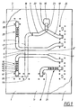
- the wave guide arrangement according to the invention is a plate structure, consisting of a body plate 1, which on its opposite sides or main surfaces is mainly or partially covered by two covering plates 2, 3, one covering plate on each side.
- the body plate is thus essentially plate shaped, and is arranged to house a number of the wave guides or other microwave components which, by different shaping of cavities, i.e. holes, in the covering plate, and connection of the covering plates 2, 3, form the different microwave components with separate functions.
- the body plate 1 is preferably given such a thickness that it allows wave guides to be separated from each other even when crossing each other, see for example locations 4 and 5 in Fig. 1.
- the wave guides in the body plate 1 consist both of wave guide grooves 6, 7, 8, 9, 10, 17 which extend along either of the main surfaces 11, 12 of the body plate 1 which surfaces usually are parallel to each other, and of wave guide sections 13, which extend at an angle relative to the main surfaces 11, 12, for example a straight angle, and with openings 14 end in either of the main surfaces 11, 12 and which by means of a through-going opening 15 in either of the covering plate 2, 3 end with an opening 16 in its outer surface 30.
- a separate component for example a microwave hybrid with an amplifier, a mixer, receiver protection, or an electrical switch.
- the wave guide grooves 6-10, 17 in the main surfaces 11, 12 are preferably obtained by means of milling, so that the grooves obtain an essentially rectangular cross section.
- the wave guide sections 13, the main extension or perpendicular direction of which forms an angle, for example a straight angle, against the main surfaces 11, 12 are formed in the body plate 1, and the covering plates 2, 3 by means of milling in the same step of production.
- Fig. 1 shows an example of a plate structure where the main part of one covering plate 2 is shown removed, so that the main part of the body plate 1 is seen from its one main surface 11, so that the different wave guide grooves 6-10 on the one side of the body plate, and a number of microwave components are visible.
- the body plate 1 is in Fig. 1 removed in the upper left corner, thus causing the opposed covering plate 3 to be seen.
- the wave guides formed by the wave guide grooves 6-10 with the corresponding covering plate 2, 3, and the angled wave guide sections 13 have the purpose of forming transmission means for microwaves between different microwave components.
- the wave guide grooves 6-10 are thus arranged in the one main surface 11 of the body plate 1 while sections of the wave guide groove 17 are arranged in the opposed main surface 12 of the body plate, and is therefore indicated with lines with dots.
- One and the same wave guide can, via wave guide bends 18, pass from one main surface 11 of the body plate (see for example wave guide groove 9) to its other main surface 12 (see for example wave guide groove 17), whereby the above mentioned crossings 4, 5, can be made in different planes. In this way, the constructions of circuits is facilitated, and a very compact construction is enabled.
- the wave guides 6-10, 17, are primarily given simple geometrical shapes in order to transmit microwave signals with a minimum of attenuation and distortion. As far as possible, they extend in a straight line, with straight sections to which are added so called H-bends and E-bends, depending on whether the change of direction of the wave guides is in the plane of the main surfaces or at an angle to it.
- Fig. 1 shows a number of a different H-bends 6', 6", which are 90° and 30°.
- the shape and the angles can be chosen from a large number of alternatives, according to what is necessary.
- the plate structure according to the present invention makes it possible to integrate several microwave components for the processing of the microwave signals in the body plate 1 and the covering plates 2, 3.
- An example apart from the wave guide is shown in Fig. 1, in the shape of filter components 19, 20, 21, the construction of which is shown in detail by means of an example in Fig. 5, which will be described further below.
- Fig. 1 shows a further example of a microwave component in the shape of a circulator 22, arranged in a branching of the wave guides 9, 10, 23.
- E-bends 18, 24 which are used either when the wave guide grooves pass from one main surface 11 to the other main surface 12, or to an opening in either of the covering plates 2, 3.
- Separate wave guide components, not shown in Fig. 1, are intended to be connected to these openings, usually by means of flanges.
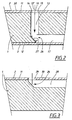
- FIG. 2 shows an example of one of the wave guide bends 26 here called a deep E-bend, and which here leads a wave guide screw in one main surface 12 of the body plate 1 across to its opposed main surface 11, via the wave guide section 13.
- the bend has a sloping surface 27. This is produced by letting a rotating cylindrical mill first be moved in the direction of the arrow 13', down into the body plate 1, after which it is moved in parallel along a chosen angle sideways up to the groove 17.
- Fig. 3 shows a so called short E-bend 24, see also Fig. 1, which is used when a wave guide groove 28 opens in the main surface 11, on that side of the covering plate 1 along which the groove extends.
- a connecting opening 29 leads the wave guide to the outwards facing surface 30 of the covering plate 2, on which the separate microwave components can be connected.
- Fig. 4 can essentially be seen as a cross section of the bend 18 according to Fig. 1, although the surrounding wave guides extend differently.
- This design is used when, for example, the wave guide groove 9 which extends along the one main surface 11 of the body plate crosses to the wave guide groove 17 which extends along the opposite main surface 12.
- the bend is a double bend, with a first bend 31 arranged in connection to the one main surface 11 of the body plate 1, and a second bend 32 arranged in connection to the other main surface 12.
- a wave guide section 33 extends between the two bends at an angle to the main surfaces, which, in the example, shown is a straight angle.
- a loose bend element 33 which has been mounted in a recess 34 in the body plate 1, subsequent to the manufacturing of the wave guide section 33 by, for example, milling, in the direction from the one main surface 11 of the body plate 1, in the manner which has been described above with reference to Fig. 2.
- bends 37, 38 also at the outer ends of the wave guide grooves 9, 10. These connect to respective connection openings 39, 40 in their corresponding covering plate 2, 3, on which, as has been mentioned above, other separate microwave components can be connected for processing of the microwave signals which are transmitted in the wave guides in the plate structure.
- the cross section according to Fig. 5 can essentially be seen as a cross section through any of the filter components 19, 20, 21, although the surrounding wave guides are of a different extension.
- the filter component is fully integrated in the plate structure, to be more precise, in the body plate 1.
- the plate structure is here shown with only one covering plate 3 in this particular part. This is due to the fact that the opposite covering plate 2 does not need to cover the entire surface of the body plate, but can be so arranged that it covers only a limited part of one of its two main surfaces 11, 12.
- the covering plates can be so arranged that there are several smaller covering plates, which can be arranged in different places on the main surfaces, or in a recessed portion in the main surfaces where the recess preferably corresponds to the thickness of the covering plate, so that a smooth and essentially plane outer surface is obtained, which in turn can support separate components.
- the functions of the band pass filter have been partially obtained by forming cavities in the body plate 1.
- a plurality of plates 41, 42 in the filter which, for example, is a band pass filter which has been formed by protruding wall sections arranged in pairs facing each other, thus forming cavities 43.
- a plurality of trim screws 44, 45 are arranged for adjustment of the filter.
- the trim screws are of two kinds, first such trim screws as 44, which are arranged between the plates to adjust the impedance and also such plates as 45, which are arranged in the cavities for adjustment of the frequency.
- the trim screws in various degrees form portions 46 which protrude downwards, and which change the mentioned filter characteristics, and thereby the electrical characteristics of the wave guides.
- Each trim screw is thus equipped with a thread, and can be displaced in the direction of its extension in threaded drill holes in the body plate 1, and are also equipped with a head 47, and a locking nut 47', arranged in a recessed section 48 of the body plate.
- the head 47 and the locking 47' nuts can be accessed from the one main surface 11 using a trim screw driver.
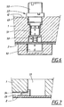
- Fig. 6 shows an example of the integration of a circulator 22, see also Fig. 1.
- the purpose of the circulator is to together with a branching, enable isolation of at least one path of transmission depending on which direction the microwave energy is received in. This is used in order to separate paths of transmission of, for example, transmitted respectively received signal, so that the receiver to a high degree is isolated from the transmitted microwave energy, which is at a considerably higher level than the energy level received.
- the circulator 22 is for example of the ferrite circulator kind, mounted in a bore 49 in the body plate 1 and encases a first magnet 51 and protrudes with a section 50 from the body plate.
- the circulator also comprises a second magnet 52.
- the circulator further protrudes downwards with a portion 53, which contains ferrite cores in the branching point of the three wave guides grooves 9, 10, 23. This part of the body plate 1 is also without the one covering plate 3 in the example shown.
- Fig. 7 shows a termination element 54 for the attenuation of reflections in a wave guide groove 23, which is another example of a microwave component which can be, in a simple way, assembled on, and integrated in the plate structure, more precisely in a recess 55 in the body plate 1. On one side of this, one of the covering plates 3 is arranged.
- Fig. 8 shows, in a perspective view, an example of a complete microwave module constructed with the plate structure according to the invention. From this, it will come apparent that the plate structure, apart from the above described construction with integrated microwave components in the structure itself, also supports separate microwave components, which are arranged on the top side or bottom side of the body plate 1 and/or the covering plates 2, 3.
- the separate microwave components can be such that they are easily replaceable. They can be preproduced standard components or can be of such a design that they cannot be integrated into the plate structure, they can be so called microwave hybrids, and thus not be only wave guide components etc.
- the entire unit can be made especially easy to handle by equipping it with carrying handles 56, 57, as in the example shown, which makes the unit easy to move for service etc, and which, at the same time constitutes a protection for microwave components.
- the unit can be mounted in, for example, a rack with several units, and can be mounted vertically, horizontally or at a sloping angle to the vertical plane.
- the production of the plate structure according to the invention can be summed up in the following way.
- the initial material for the body plate 1 is a massive plate of an electrically conducting material, for example aluminum or an alloy of it.
- the plate has, for example, rectangular surfaces with its two main surfaces 11, 12 plane and parallel, possibly with stepwise changes in level.
- the thickness of the body plate i.e. the distance between the main surfaces 11, 12 at least in the crossings exceeds double the depth of the wave guide grooves.
- the wave guide grooves are made by a for example, computer controlled mill, which can be of different kinds, with a cylindrical rotating milling head which creates a mainly rectangular profile shape with perpendicular side edges and a plane bottom.
- the wave guide grooves are preferably milled on both sides of the body plate, i.e. in its two main surfaces 11, 12.
- the wave guide sections which are at an angle to the main surfaces are then made at predetermined positions by means of milling. All the bends are made with their specially designed surfaces.
- the covering plates 2, 3 can be made separately from the body plate, by drilling or milling in order to create attachment holes or connection openings. Alternatively, this can be done at a later stage after the covering plates have been connected to the body plate.
- the covering plates 2, 3 are connected to the body plate subsequent to placing a very carefully measured amount of solder between the covering plates and the body plate, after which the covering plates by means of salt bath soldering are solded together with the body plate, so that the wave guide grooves in the main surfaces obtain predetermined crosswise dimensions.
- microwave components can both be integrated and/or supported by the structure.
- examples of such components are variable attenuators, other kinds of filters such as low pass and high pass filters, isolators, power splitters, directional couplers etc.
Landscapes
- Engineering & Computer Science (AREA)
- Manufacturing & Machinery (AREA)
- Control Of Motors That Do Not Use Commutators (AREA)
- Waveguides (AREA)
Description
- The present invention relates to a wave guide arrangement for the transmission and processing of microwave signals, comprising a plate structure with recesses which form wave guides, for the transmission of microwave signals between microwave components, wherein said plate structure is formed by an electrically conductive body plate and at least two electrically conductive covering plates for at least partial connection to two opposite surfaces of the body plate, and in that both the body plate and the covering plates form delimiting surfaces for at least a part of the wave guides, and in that at least part of said microwave components are arranged in the body plate and/or the covering plates.
- The present invention also relates to a method for producing a wave guide arrangement for the transmission and processing of microwave signals.
- The traditional way of producing microwave components is to produce each component, such as wave guide filters, circulators, etc., separately, and then to join them to each other, using a number of separate wave guide elements on a supporting structure or mounting plate. This technique demands a great deal of space, is expensive, and results in a large amount of connections which are imperfect, with the risk of negative influence on the function.
- The Derwent's abstract, No. 88-90824/13, week 8813; & SU-A1334226, (AS UKR RADIOPHYS EL) 30-08-1987 describes how two opposite walls of a wave guide are formed by cutting through a first metal plate. A second and third metal plate are secured to opposing sides of the first plate, thus forming a third and fourth wall, respectively, for the waveguide.
- EP-A-319 629 describes a transition between two orthogonal waveguides, by way of example from a horizontal waveguide to a vertical waveguide. The transition is applicable for microwave frequencies, i.e. millimetre-waves.
- The object of the present invention is to obtain a wave guide means and a method of production, by means of which is achieved a compact construction technique with small tolerances and fewer steps of manual assembly.
- The wave guide arrangement according to the invention is characterized in that at least part of the wave guides, is formed mainly by grooves in the opposite surfaces of the body plate which grooves end in connection openings for the microwave signals in their respective covering plate.
- The method according to the invention is characterized by the following steps:
- Making wave guide grooves in the main surfaces of an electrically conducting body plate,
- making connection openings for the microwave signals in electrically conducting covering plates and
- sealing the wave guide grooves by attaching the covering plates against the side surfaces of the body plate, whereby wave guides are formed.
-
- An advantage of the invention is that the plate structure can both enclose microwave component, and can also support microwave components. In this way, compact, stable, and small units can be built in a cost efficient way.
- The invention will in the following be described in detail by means of embodiments, with reference to the appended drawings in which,
- Fig. 1 shows an example of a wave guide arrangement according to the present invention,
- Fig. 2 in a larger scale shows a cross-section of the wave guide arrangement according to the invention in a part which has a wave guide component in the shape of a deep E-bend,
- Fig. 3 shows a cross-section of a wave guide arrangement in a part which has a wave guide component in the shape of a short E-bend,
- Fig. 4 is a cross section through the wave guide arrangement to the invention, which shows a wave guide component in the form of a so called separate bend element.
- Fig. 5 is a cross section through the wave guide arrangement, which shows an example of a micro wave component which is a band pass filter.
- Fig. 6 is a cross section of the wave guide arrangement in the shape of a microwave component which is a circulator insert, while
- Fig. 7 is a cross section through a wave guide component in the shape of a termination, and
- Fig. 8 is a perspective view of a complete unit with a wave guide arrangement, as well as other components mounted on it.
-
- As can for example be seen from Figs. 1 and 2, the wave guide arrangement according to the invention is a plate structure, consisting of a
body plate 1, which on its opposite sides or main surfaces is mainly or partially covered by twocovering plates covering plates body plate 1 is preferably given such a thickness that it allows wave guides to be separated from each other even when crossing each other, see for example locations 4 and 5 in Fig. 1. The wave guides in thebody plate 1 consist both ofwave guide grooves main surfaces body plate 1 which surfaces usually are parallel to each other, and ofwave guide sections 13, which extend at an angle relative to themain surfaces openings 14 end in either of themain surfaces covering plate opening 16 in itsouter surface 30. In connection to theopening 16 there is usually arranged a separate component, for example a microwave hybrid with an amplifier, a mixer, receiver protection, or an electrical switch. The wave guide grooves 6-10, 17 in themain surfaces wave guide sections 13, the main extension or perpendicular direction of which forms an angle, for example a straight angle, against themain surfaces body plate 1, and thecovering plates - Fig. 1 shows an example of a plate structure where the main part of one
covering plate 2 is shown removed, so that the main part of thebody plate 1 is seen from its onemain surface 11, so that the different wave guide grooves 6-10 on the one side of the body plate, and a number of microwave components are visible. Thebody plate 1 is in Fig. 1 removed in the upper left corner, thus causing theopposed covering plate 3 to be seen. The wave guides formed by the wave guide grooves 6-10 with thecorresponding covering plate wave guide sections 13 have the purpose of forming transmission means for microwaves between different microwave components. The wave guide grooves 6-10, shown with solid lines, are thus arranged in the onemain surface 11 of thebody plate 1 while sections of thewave guide groove 17 are arranged in the opposedmain surface 12 of the body plate, and is therefore indicated with lines with dots. One and the same wave guide can, viawave guide bends 18, pass from onemain surface 11 of the body plate (see for example wave guide groove 9) to its other main surface 12 (see for example wave guide groove 17), whereby the above mentioned crossings 4, 5, can be made in different planes. In this way, the constructions of circuits is facilitated, and a very compact construction is enabled. The wave guides 6-10, 17, are primarily given simple geometrical shapes in order to transmit microwave signals with a minimum of attenuation and distortion. As far as possible, they extend in a straight line, with straight sections to which are added so called H-bends and E-bends, depending on whether the change of direction of the wave guides is in the plane of the main surfaces or at an angle to it. - Fig. 1 shows a number of a different H-
bends 6', 6", which are 90° and 30°. The shape and the angles can be chosen from a large number of alternatives, according to what is necessary. - As mentioned above, the plate structure according to the present invention makes it possible to integrate several microwave components for the processing of the microwave signals in the
body plate 1 and thecovering plates filter components - From Fig. 1 it will become apparent that the
filter components circulator 22, arranged in a branching of thewave guides E-bends main surface 11 to the othermain surface 12, or to an opening in either of thecovering plates respective covering plates body plate 1, in which there is arranged a number ofscrew holes 25 around each opening. Fig. 2 shows an example of one of thewave guide bends 26 here called a deep E-bend, and which here leads a wave guide screw in onemain surface 12 of thebody plate 1 across to its opposedmain surface 11, via thewave guide section 13. In order to achieve good transmission of the microwave signals in the wave guide, the bend has a slopingsurface 27. This is produced by letting a rotating cylindrical mill first be moved in the direction of the arrow 13', down into thebody plate 1, after which it is moved in parallel along a chosen angle sideways up to thegroove 17. - The example in Fig. 3 shows a so called
short E-bend 24, see also Fig. 1, which is used when awave guide groove 28 opens in themain surface 11, on that side of thecovering plate 1 along which the groove extends. A connectingopening 29 leads the wave guide to the outwards facingsurface 30 of thecovering plate 2, on which the separate microwave components can be connected. - Fig. 4 can essentially be seen as a cross section of the
bend 18 according to Fig. 1, although the surrounding wave guides extend differently. This design is used when, for example, thewave guide groove 9 which extends along the onemain surface 11 of the body plate crosses to thewave guide groove 17 which extends along the oppositemain surface 12. As can be seen from the figure, the bend is a double bend, with a first bend 31 arranged in connection to the onemain surface 11 of thebody plate 1, and asecond bend 32 arranged in connection to the othermain surface 12. A wave guide section 33 extends between the two bends at an angle to the main surfaces, which, in the example, shown is a straight angle. For reasons of production, there is in connection to the one bend 31 arranged a loose bend element 33, which has been mounted in a recess 34 in thebody plate 1, subsequent to the manufacturing of the wave guide section 33 by, for example, milling, in the direction from the onemain surface 11 of thebody plate 1, in the manner which has been described above with reference to Fig. 2. In the example shown in Fig. 4 there arebends wave guide grooves respective connection openings corresponding covering plate - The cross section according to Fig. 5 can essentially be seen as a cross section through any of the
filter components body plate 1. The plate structure is here shown with only onecovering plate 3 in this particular part. This is due to the fact that theopposite covering plate 2 does not need to cover the entire surface of the body plate, but can be so arranged that it covers only a limited part of one of its twomain surfaces body plate 1. Thus, there is arranged a plurality ofplates 41, 42 in the filter which, for example, is a band pass filter which has been formed by protruding wall sections arranged in pairs facing each other, thus forming cavities 43. A plurality oftrim screws portions 46 which protrude downwards, and which change the mentioned filter characteristics, and thereby the electrical characteristics of the wave guides. Each trim screw is thus equipped with a thread, and can be displaced in the direction of its extension in threaded drill holes in thebody plate 1, and are also equipped with ahead 47, and a locking nut 47', arranged in a recessedsection 48 of the body plate. Thehead 47 and the locking 47' nuts can be accessed from the onemain surface 11 using a trim screw driver. - Fig. 6 shows an example of the integration of a
circulator 22, see also Fig. 1. The purpose of the circulator is to together with a branching, enable isolation of at least one path of transmission depending on which direction the microwave energy is received in. This is used in order to separate paths of transmission of, for example, transmitted respectively received signal, so that the receiver to a high degree is isolated from the transmitted microwave energy, which is at a considerably higher level than the energy level received. From Fig. 6 it will become apparent that thecirculator 22 is for example of the ferrite circulator kind, mounted in abore 49 in thebody plate 1 and encases afirst magnet 51 and protrudes with asection 50 from the body plate. The circulator also comprises asecond magnet 52. The circulator further protrudes downwards with aportion 53, which contains ferrite cores in the branching point of the threewave guides grooves body plate 1 is also without the onecovering plate 3 in the example shown. - Fig. 7 shows a
termination element 54 for the attenuation of reflections in awave guide groove 23, which is another example of a microwave component which can be, in a simple way, assembled on, and integrated in the plate structure, more precisely in arecess 55 in thebody plate 1. On one side of this, one of the coveringplates 3 is arranged. - Fig. 8 shows, in a perspective view, an example of a complete microwave module constructed with the plate structure according to the invention. From this, it will come apparent that the plate structure, apart from the above described construction with integrated microwave components in the structure itself, also supports separate microwave components, which are arranged on the top side or bottom side of the
body plate 1 and/or the coveringplates handles - The production of the plate structure according to the invention can be summed up in the following way. The initial material for the
body plate 1 is a massive plate of an electrically conducting material, for example aluminum or an alloy of it. The plate has, for example, rectangular surfaces with its twomain surfaces main surfaces main surfaces - The covering
plates - The covering
plates - The invention is not limited to the embodiments described above and shown in the examples, but can be varied within the scope of the appended patent claims. For example, completely different microwave components can both be integrated and/or supported by the structure. Examples of such components are variable attenuators, other kinds of filters such as low pass and high pass filters, isolators, power splitters, directional couplers etc.
Claims (15)
- A wave guide arrangement for the transmission and processing of microwave signals, comprising a plate structure with recesses which form wave guides (6, 10), (13, 17, 28), for the transmission of microwave signals between microwave components (19, 20, 21, 22), wherein said plate structure is formed by an electrically conductive body plate (1) and at least two electrically conductive covering plates (2, 3) for at least partial connection to two opposite surfaces (11, 12) of the body plate, and in that both the body plate and the covering plates form delimiting surfaces for at least a part of the wave guides (6-10, 17-28), and in that at least part of said microwave components are arranged in the body plate and/or the covering plates, characterized in that at least part of the wave guides (6-10, 17, 28) is formed mainly by grooves in the opposite surfaces of the body plate which grooves end in connection openings (15, 29) for the microwave signals in their respective covering plate.
- Wave guide arrangement according to claim 1,
characterized in that the wave guides comprise wave guide sections (13, 33) which connect to the wave guide grooves and extend at an angle relative to the opposite surfaces of the body plate (1). - Wave guide arrangement according to claim 2,
characterized in that the wave guides comprise wave guide bends (24, 26, 31, 32) which are made by shaping the wave guide grooves in the body plate (1) and their connections to said wave guide sections (13). - Wave guide arrangement according to claim 3,
characterized in that at least one of said connection openings (29) is arranged in connection to that surface (11) of the body plate (1) where the corresponding wave guide groove (28) has been shaped, and in that, for the connection of said groove to said connection opening, one of said bends (24) is arranged at the surface where the groove has been shaped. - Wave guide arrangement according to claim 3,
characterized in that at least one of said connection openings (15) is arranged in connection to that surface (12) of the body plate (1) which is opposite to that surface (11) where the corresponding wave guide groove (17) has been shaped, and in that, for the connection of said groove to said connection opening, one of said bends (26) is arranged in the area of the same surface as where the groove has been shaped. - Wave guide arrangement according to claim 2,
characterized in that said connection between said wave guide sections (33) and the wave guide grooves (9-17) is achieved by means of wave guide bends (31, 32) of which at least one bend is arranged at a distance from one of said connection openings (39), and is formed by a separate bend element (31') positioned in a recess (34) in the body plate (11). - Wave guide arrangement according to claim 5,
characterized in that at least one of the wave guide grooves (23) is terminated by means of a separate termination element (54) arranged to seal one end of the groove between the body plate (1) and its corresponding covering plate (3). - Wave guide arrangement according to claim 6,
characterized in that said separate bend element (31') forms one bend (31) in a double bend (18) for the transition between wave guide grooves (9, 17) in the two opposite surfaces (11, 12) of the body plate, where one of the bends is positioned at one of the surfaces and the other bend (32) is positioned at the other surface. - Wave guide arrangement according to claim 1,
characterized in that at least one of the microwave components is a circulator (22) positioned in a recess (49) which extends between the one wall (12) of the body plate (1) to a branching point of any of the wave guide grooves (9, 10, 23) in the opposite surface (11). - Wave guide arrangement according to claim 1,
characterized in that said microwave components (19-22) in the body plate (1) are formed in the body plate. - Wave guide arrangement according to claim 10,
characterized in that at least one of said microwave components is a filter component (19, 20, 21) formed by a plurality of fixed plates (41, 42) arranged in the body plate (1). - Wave guide arrangement according to claim 11,
characterized in that said filter component (19, 20, 21) comprises a plurality of trim screws (45) arranged in bores in the body plate (1), and which are accessible from the one surface (11) of the body plate (1), and which are adapted to adjust said filter component. - Method for producing a wave guide arrangement for the transmission and processing of microwave signals,
characterized by the following steps:Making wave guide grooves (6-10, 17, 28) in the two opposite main surfaces (11, 12) of an electrically conducting body plate (1),making connection openings (15, 29) for the microwave signals in two electrically conducting covering plates (2, 3) andsealing the wave guide grooves by attaching the covering plates against the main surfaces of the body plate, whereby wave guides are formed. - Method according to claim 13,
characterized in that the wave guides (6-10, 13, 17, 28) are made by mechanical means, such as milling. - Method according to claim 14,
characterized in that the attachment of the covering plates to the body plate is done by means of salt bath soldering.
Applications Claiming Priority (2)
| Application Number | Priority Date | Filing Date | Title |
|---|---|---|---|
| SE9601955A SE505504C2 (en) | 1996-05-23 | 1996-05-23 | Waveguide device and method for its manufacture |
| SE9601955 | 1996-05-23 |
Publications (2)
| Publication Number | Publication Date |
|---|---|
| EP0809319A1 EP0809319A1 (en) | 1997-11-26 |
| EP0809319B1 true EP0809319B1 (en) | 2003-03-26 |
Family
ID=20402658
Family Applications (1)
| Application Number | Title | Priority Date | Filing Date |
|---|---|---|---|
| EP97850080A Expired - Lifetime EP0809319B1 (en) | 1996-05-23 | 1997-05-22 | Wave guide arrangement and a method for producing it |
Country Status (4)
| Country | Link |
|---|---|
| US (1) | US6011453A (en) |
| EP (1) | EP0809319B1 (en) |
| DE (1) | DE69720105T2 (en) |
| SE (1) | SE505504C2 (en) |
Families Citing this family (9)
| Publication number | Priority date | Publication date | Assignee | Title |
|---|---|---|---|---|
| SE513586C2 (en) * | 1998-05-12 | 2000-10-02 | Ericsson Telefon Ab L M | Method of producing an antenna structure and antenna structure prepared by said method |
| CN100352793C (en) * | 2006-01-20 | 2007-12-05 | 杨鸿生 | Groove waveguide microwave chemical reaction equipment for ethene preparation by natural gas and preparation method thereof |
| GB2434923A (en) * | 2006-02-03 | 2007-08-08 | Ericsson Telefon Ab L M | Antenna feed device using two separate L-shaped waveguides to give an overall T-shape |
| US7630696B2 (en) | 2006-06-16 | 2009-12-08 | At&T Mobility Ii Llc | Multi-band RF combiner |
| CA2648256A1 (en) * | 2006-06-16 | 2008-02-28 | Cingular Wireless Ii, Llc | Multi-resonant microstrip dipole antenna |
| US7764245B2 (en) | 2006-06-16 | 2010-07-27 | Cingular Wireless Ii, Llc | Multi-band antenna |
| US7277062B1 (en) | 2006-06-16 | 2007-10-02 | At&T Mobility Ii Llc | Multi-resonant microstrip dipole antenna |
| US10403956B2 (en) * | 2016-10-04 | 2019-09-03 | The Boeing Company | Simplification of complex waveguide networks |
| US11506686B2 (en) * | 2019-11-25 | 2022-11-22 | Advantest Corporation | High density waveguide assembly for millimeter and 5G applications |
Family Cites Families (10)
| Publication number | Priority date | Publication date | Assignee | Title |
|---|---|---|---|---|
| US3292115A (en) * | 1964-09-11 | 1966-12-13 | Hazeltine Research Inc | Easily fabricated waveguide structures |
| US3686596A (en) * | 1971-03-08 | 1972-08-22 | Bunker Ramo | Double mitered compensated waveguide bend |
| JPS62141801A (en) * | 1985-12-16 | 1987-06-25 | Nec Corp | Waveguide circuit |
| FR2605147B1 (en) * | 1986-10-10 | 1988-12-02 | Thomson Csf | METHOD FOR PROVIDING A MICROWAVE TRANSITION BETWEEN TWO ORTHOGONAL GUIDED STRUCTURES AND MICROWAVE CIRCUIT HAVING SUCH A TRANSITION |
| US4812789A (en) * | 1987-10-05 | 1989-03-14 | Hughes Aircraft Company | Ridged waveguide wide band diplexer with extremely sharp cut-off properties |
| JPH04299601A (en) * | 1991-03-28 | 1992-10-22 | Nec Corp | Band obstructing filter |
| SE469540B (en) * | 1991-11-29 | 1993-07-19 | Ericsson Telefon Ab L M | GUIDANCE GUARANTEE WITH TARGETED HALL ROOM GUARD |
| US5381596A (en) * | 1993-02-23 | 1995-01-17 | E-Systems, Inc. | Apparatus and method of manufacturing a 3-dimensional waveguide |
| SE502441C2 (en) * | 1994-02-02 | 1995-10-16 | Ericsson Telefon Ab L M | Device for storing four microwave signals and magic T for use in the device |
| US5581217A (en) * | 1995-09-21 | 1996-12-03 | Hughes Aircraft Company | Microwave shielding structures comprising parallel-plate waveguide |
-
1996
- 1996-05-23 SE SE9601955A patent/SE505504C2/en unknown
-
1997
- 1997-05-22 DE DE69720105T patent/DE69720105T2/en not_active Expired - Lifetime
- 1997-05-22 US US08/862,031 patent/US6011453A/en not_active Expired - Lifetime
- 1997-05-22 EP EP97850080A patent/EP0809319B1/en not_active Expired - Lifetime
Also Published As
| Publication number | Publication date |
|---|---|
| SE9601955L (en) | 1997-09-08 |
| SE9601955D0 (en) | 1996-05-23 |
| DE69720105D1 (en) | 2003-04-30 |
| DE69720105T2 (en) | 2004-02-05 |
| EP0809319A1 (en) | 1997-11-26 |
| US6011453A (en) | 2000-01-04 |
| SE505504C2 (en) | 1997-09-08 |
Similar Documents
| Publication | Publication Date | Title |
|---|---|---|
| US10879576B2 (en) | Filter assemblies, tuning elements and method of tuning a filter | |
| EP3375036B1 (en) | Filter assemblies, tuning elements | |
| US11495871B2 (en) | Waveguide device having multiple layers, where through going empty holes are in each layer and are offset in adjoining layers for leakage suppression | |
| CA1212432A (en) | Microwave circuit device and method for fabrication | |
| EP0809319B1 (en) | Wave guide arrangement and a method for producing it | |
| EP1646105A1 (en) | Filter assemblies and communication systems based thereon | |
| CN106848510A (en) | A kind of dual-passband difference filter of laminate substrate integrated wave guide structure | |
| US5905416A (en) | Die-cast duplexer | |
| US7002433B2 (en) | Microwave coupler | |
| US6842085B2 (en) | Orthomode transducer having improved cross-polarization suppression and method of manufacture | |
| US6956449B2 (en) | Quadrature hybrid low loss directional coupler | |
| US6523248B1 (en) | Method of producing a microwave filter | |
| EP1324419B1 (en) | System for cross-coupling resonators | |
| US4210880A (en) | Multiple branch-line wave guide coupler | |
| WO2022257018A1 (en) | A dielectric waveguide port coupling structure, a dielectric waveguide filter, a duplexer and a multiplexer | |
| CN108879098B (en) | Microstrip line 2 x 4butler matrix with band-pass filtering characteristic | |
| EP3490055A1 (en) | A multi-mode cavity filter | |
| CN110994098A (en) | Tapered resonator based on cavity filter | |
| Aljarosha | Millimeter-wave microstrip-to-groove gap waveguide transition for use in gap-waveguide-integrated grid amplifiers and antenna arrays | |
| CN115051133B (en) | Waveguide broadside broadband coupling bridge | |
| US6657521B2 (en) | Microwave waveguide filter having rectangular cavities, and method for its fabrication | |
| EP4298688A1 (en) | Very efficient 5g/6g antenna array system (aas) feed structures | |
| CA2086060C (en) | Broadband directional coupler using cables |
Legal Events
| Date | Code | Title | Description |
|---|---|---|---|
| PUAI | Public reference made under article 153(3) epc to a published international application that has entered the european phase |
Free format text: ORIGINAL CODE: 0009012 |
|
| AK | Designated contracting states |
Kind code of ref document: A1 Designated state(s): DE DK FI FR GB NL |
|
| 17P | Request for examination filed |
Effective date: 19980526 |
|
| AKX | Designation fees paid |
Free format text: DE DK FI FR GB NL |
|
| RBV | Designated contracting states (corrected) |
Designated state(s): DE DK FI FR GB NL |
|
| 17Q | First examination report despatched |
Effective date: 20011108 |
|
| GRAG | Despatch of communication of intention to grant |
Free format text: ORIGINAL CODE: EPIDOS AGRA |
|
| GRAG | Despatch of communication of intention to grant |
Free format text: ORIGINAL CODE: EPIDOS AGRA |
|
| GRAH | Despatch of communication of intention to grant a patent |
Free format text: ORIGINAL CODE: EPIDOS IGRA |
|
| GRAH | Despatch of communication of intention to grant a patent |
Free format text: ORIGINAL CODE: EPIDOS IGRA |
|
| GRAA | (expected) grant |
Free format text: ORIGINAL CODE: 0009210 |
|
| AK | Designated contracting states |
Designated state(s): DE DK FI FR GB NL |
|
| PG25 | Lapsed in a contracting state [announced via postgrant information from national office to epo] |
Ref country code: NL Free format text: LAPSE BECAUSE OF FAILURE TO SUBMIT A TRANSLATION OF THE DESCRIPTION OR TO PAY THE FEE WITHIN THE PRESCRIBED TIME-LIMIT Effective date: 20030326 Ref country code: FR Free format text: LAPSE BECAUSE OF FAILURE TO SUBMIT A TRANSLATION OF THE DESCRIPTION OR TO PAY THE FEE WITHIN THE PRESCRIBED TIME-LIMIT Effective date: 20030326 Ref country code: FI Free format text: LAPSE BECAUSE OF FAILURE TO SUBMIT A TRANSLATION OF THE DESCRIPTION OR TO PAY THE FEE WITHIN THE PRESCRIBED TIME-LIMIT Effective date: 20030326 |
|
| REG | Reference to a national code |
Ref country code: GB Ref legal event code: FG4D |
|
| REF | Corresponds to: |
Ref document number: 69720105 Country of ref document: DE Date of ref document: 20030430 Kind code of ref document: P |
|
| PG25 | Lapsed in a contracting state [announced via postgrant information from national office to epo] |
Ref country code: DK Free format text: LAPSE BECAUSE OF FAILURE TO SUBMIT A TRANSLATION OF THE DESCRIPTION OR TO PAY THE FEE WITHIN THE PRESCRIBED TIME-LIMIT Effective date: 20030626 |
|
| NLV1 | Nl: lapsed or annulled due to failure to fulfill the requirements of art. 29p and 29m of the patents act | ||
| PLBE | No opposition filed within time limit |
Free format text: ORIGINAL CODE: 0009261 |
|
| STAA | Information on the status of an ep patent application or granted ep patent |
Free format text: STATUS: NO OPPOSITION FILED WITHIN TIME LIMIT |
|
| EN | Fr: translation not filed | ||
| 26N | No opposition filed |
Effective date: 20031230 |
|
| PGFP | Annual fee paid to national office [announced via postgrant information from national office to epo] |
Ref country code: DE Payment date: 20160527 Year of fee payment: 20 Ref country code: GB Payment date: 20160527 Year of fee payment: 20 |
|
| REG | Reference to a national code |
Ref country code: DE Ref legal event code: R071 Ref document number: 69720105 Country of ref document: DE |
|
| REG | Reference to a national code |
Ref country code: GB Ref legal event code: PE20 Expiry date: 20170521 |
|
| PG25 | Lapsed in a contracting state [announced via postgrant information from national office to epo] |
Ref country code: GB Free format text: LAPSE BECAUSE OF EXPIRATION OF PROTECTION Effective date: 20170521 |